

Page 1
This well established zener diode series for the 1N3016 thru 1N3051
JEDEC registration in the metal case DO-13 package provides a glass
hermetic seal for 6.8 to 200 volts. It is also well suited for high-reliability
applications where it is available in JAN, JANTX, and JANTXV military
qualifications. Lower voltages are also available in the 1N3821 thru
1N3830 series (3.3 V to 7.5 V) in the same package (see separate data
sheet). Microsemi also offers numerous other Zener diode products for a
variety of other packages including surface mount.
SCOTTSDALE DIVISION
DESCRIPTION
1N3016B thru 1N3051B
1 WATT METAL CASE ZENER DIODES
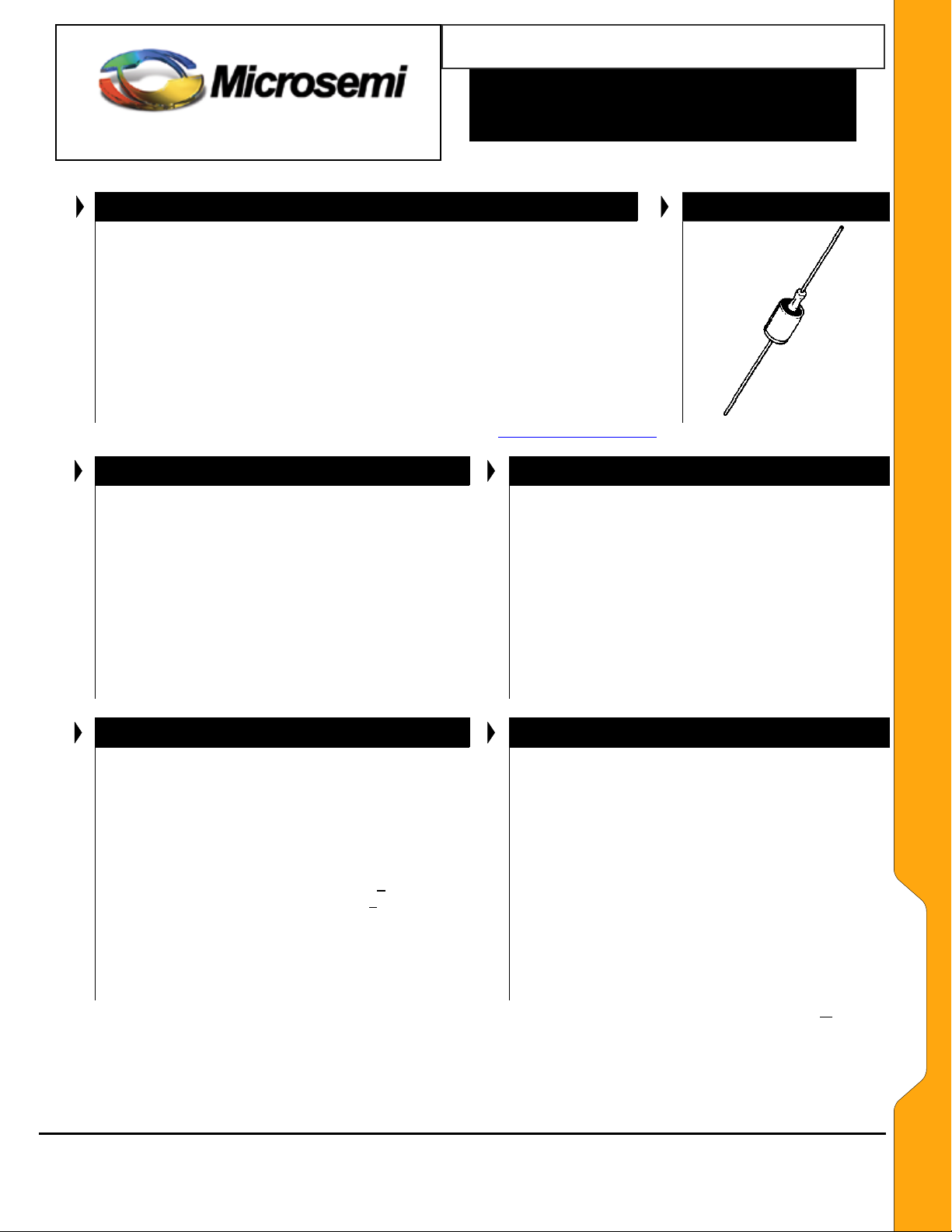
APPEARANCE
WWW.
Microsemi
. COM
IMPORTANT: For the most current data, consult
MICROSEMI’s
website: http://www.microsemi.com
• Zener Voltage Range: 6.8V to 200V
• Hermetically sealed DO-13 metal package
• Internally solder-bonded construction.
• Also available in JAN, JANTX, JANTXV
qualifications per MIL-PRF19500/115 by adding the
JAN, JANTX, or JANTXV prefixes to part numbers
for desired level of screening, e.g. JANTX1N3016B,
JANTXV1N3051B, etc.
• Surface mount also available with 1N3016BUR-1
thru 1N3051BUR-1 series on separate data sheet
FEATURES
• Regulates voltage over a broad operating current
• Wide selection from 6.8 to 200 V
• Tight voltage tolerances available
• Low reverse (leakage) currents
• Nonsensitive to ESD
• Hermetically sealed metal package
• Inherently radiation hard as described in Microsemi
APPLICATIONS / BENEFITS
and temperature range
MicroNote 050
• Operating Junction and Storage Temperatures:
-65
• THERMAL RESISTANCE: 50
at 0.375 inches (10 mm) from body or 110
junction to ambient when leads are mounted on FR4
PC board with 4 mm2 copper pads (1 oz) and track
width 1 mm, length 25 mm
• DC Power Dissipation*: 1.0 Watt at TL < +125oC 3/8”
(10 mm) from body or 1.0 Watts at T
mounted on FR4 PC board as described for thermal
resistance above (also see Fig 1)
• Forward Voltage @ 200 mA: 1.5 Volts.
• Solder Temperatures: 260
MAXIMUM RATINGS
o
C to +175oC
o
C/W* junction to lead
o
C for 10 s (maximum)
o
< +65oC when
L
C/W
MECHANICAL AND PACKAGING
• CASE: DO-13 (DO-202AA), welded, hermetically
sealed metal and glass
• FINISH: All external surfaces are Tin-Lead (Pb/Sn)
plated and solderable per MIL-STD-750 method
2026
• POLARITY: Cathode connected case.
• WEIGHT: 1.4 grams.
• Tape & Reel option: Standard per EIA-296 (add
“TR” suffix to part number)
• See package dimensions on last page
* For further mounting reference, thermal resistance from junction to metal case may be reduced to < 20
when mounting DO-13 metal case directly on heat sink.
DO-13
o
1N3016B – 1N3051B
C/W
Copyright 2003
11-03-2003 REV A
Microsemi
Scottsdale Division
8700 E. Thomas Rd. PO Box 1390, Scottsdale, AZ 85252 USA, (480) 941-6300, Fax: (480) 947-1503
Page 1
Page 2
SCOTTSDALE DIVISION
1N3016B thru 1N3051B
1 WATT METAL CASE ZENER DIODES
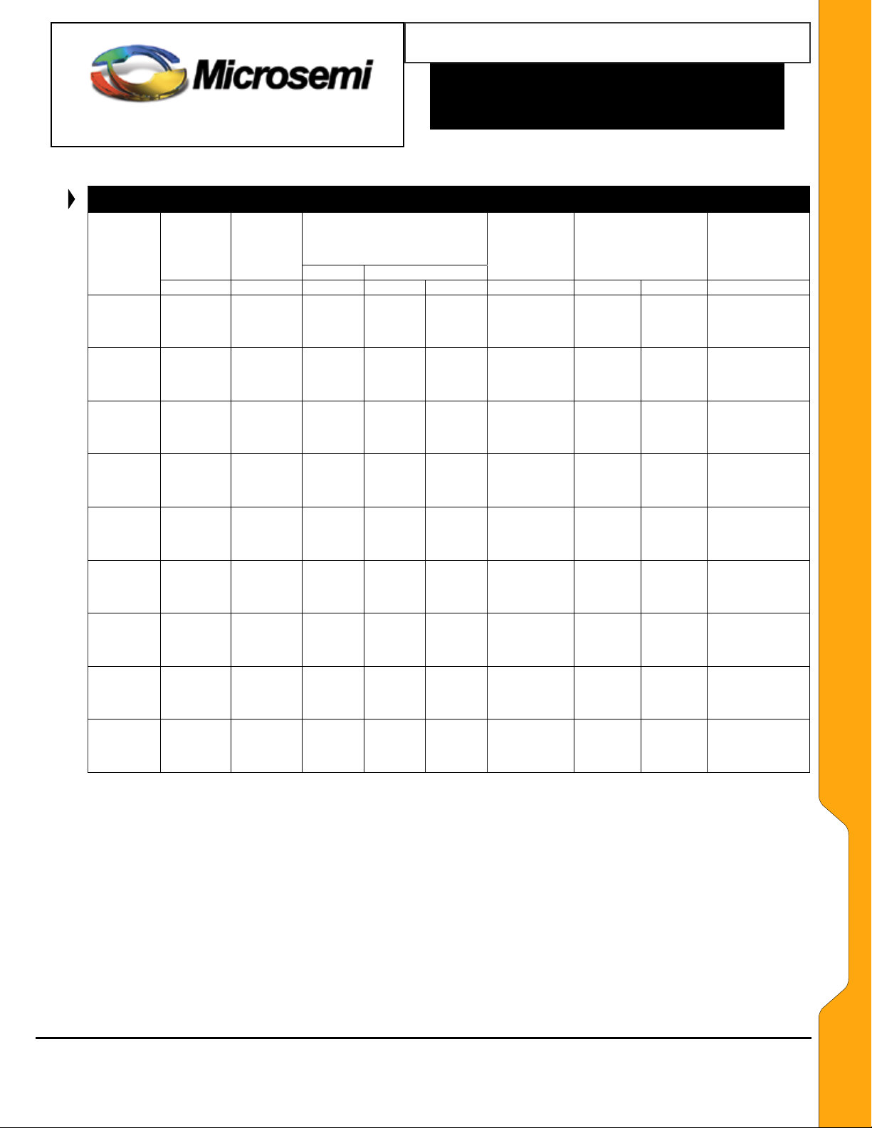
*ELECTRICAL CHARACTERISTICS @ 25oC
JEDEC
TYPE
NUMBER
(Note 1)
1N3016B
1N3017B
1N3018B
1N3019B
1N3020B
1N3021B
1N3022B
1N3023B
1N3024B
1N3025B
1N3026B
1N3027B
1N3028B
1N3029B
1N3030B
1N3031B
1N3032B
1N3033B
1N3034B
1N3035B
1N3036B
1N3037B
1N3038B
1N3039B
1N3040B
1N3041B
1N3042B
1N3043B
1N3044B
1N3045B
1N3046B
1N3047B
1N3048B
1N3049B
1N3050B
1N3051B
*JEDEC Registered Data. †Not JEDEC Data.
NOTES: 1. When using JEDEC numbers, B suffix signifies +/-5% tolerance on nominal zener voltage. The suffix A is used to identify +/-10%
tolerance; no suffix indicates +/-20% tolerance: suffix C is used to identify +/- 2%; and suffix D is used to identify +/- 1% tolerance.
NOMINAL
ZENER
VOLTAGE
@ IZT
V
Z
(Note 2)
Volts mA OHMS OHMS mA mA µA Volts %/
6.8
7.5
8.2
9.1
10
11
12
13
15
16
18
20
22
24
27
30
33
36
39
43
47
51
56
62
68
75
82
91
100
110
120
130
150
160
180
200
2. Zener Voltage (
nominal voltages provide a constant 0.25 watts.
3. The zener impedance is derived when a 60 cycle ac current having an rms value equal to 10% of the dc zener current (I
) is superimposed on IZT or IZK. Zener impedance is measured at 2 points to ensure a sharp knee on the breakdown curve
I
ZK
and to eliminate unstable units. See MicroNote 202 for variation in dynamic impedance with different zener currents.
4. These values of I
voltage end of its tolerance range. Allowance has also been made for the rise in zener voltage above V
impedance and the increase in junction temperature as a unit approaches thermal equilibrium at a dissipation of 1 watt. The IZM
values shown for +/-5% tolerance units may be used with little error for +/-10% tolerance units, but should be reduced by 7% to
include a +/-20% tolerance unit near the high voltage end of its tolerance range.
ZENER
TEST
CURRENT
I
ZT
37
34
31
28
25
23
21
19
17
15.5
14
12.5
11.5
10.5
9.5
8.5
7.5
7.0
6.5
6.0
5.5
5.0
4.5
4.0
3.7
3.3
3.0
2.8
2.5
2.3
2.0
1.9
1.7
1.6
1.4
1.2
V
) is measured with junction in thermal equilibrium with still air at a temperature of 25oC. The test currents (IZT) at
Z
may often be exceeded in the case of individual diodes. The values shown are calculated for a unit at the high
ZM
MAXIMUM ZENER IMPEDANCE
Z
@ IZT ZZK @ IZK
ZT
3.5
4.0
4.5
5
7
8
9
10
14
16
20
22
23
25
35
40
45
50
60
70
80
95
110
125
150
175
200
250
350
450
550
700
1000
1100
1200
1500
(Note 3)
700
700
700
700
700
700
700
700
700
700
750
750
750
750
750
1000
1000
1000
1000
1500
1500
1500
2000
2000
2000
2000
3000
3000
3000
4000
4500
5000
6000
6500
7000
8000
1.0
.5
.5
.5
.25
.25
.25
.25
.25
.25
.25
.25
.25
.25
.25
.25
.25
.25
.25
.25
.25
.25
.25
.25
.25
.25
.25
.25
.25
.25
.25
.25
.25
.25
.25
.25
MAXIMUM
ZENER
CURRENT
I
ZM
(Note 4)
140
125
115
105
95
85
80
74
63
60
52
47
43
40
34
31
28
26
23
21
19
18
17
15
14
12
11
10
9.0
8.3
8.0
6.9
5.7
5.4
4.9
4.6
MAXIMUM
REVERSE
LEAKAGE
CURRENT†
@ VR
I
R
150
100
50
25
25
10
10
10
10
10
10
10
10
10
10
10
10
10
10
10
10
10
10
10
10
10
10
10
10
10
10
10
10
10
10
10
TYPICAL
TEMP. COEFF.
OF ZENER
VOLTAGE
5.2
5.7
6.2
6.9
7.6
8.4
9.1
9.9
11.4
12.2
13.7
15.2
16.7
18.2
20.6
22.8
25.1
27.4
29.7
32.7
35.8
38.8
42.6
47.1
51.7
56.0
62.2
69.2
76.0
83.6
91.2
98.8
114.0
121.6
136.8
152.0
that results from zener
ZT
α
VZ
o
.040
.045
.048
.050
.055
.060
.065
.065
.070
.070
.075
.075
.080
.080
.085
.085
.085
.085
.090
.090
.090
.090
.090
.090
.090
.090
.090
.090
.090
.095
.095
.095
.095
.095
.095
.100
ZT
C
or
WWW.
Microsemi
. COM
1N3016B – 1N3051B
Copyright 2003
11-03-2003 REV A
Microsemi
Scottsdale Division
8700 E. Thomas Rd. PO Box 1390, Scottsdale, AZ 85252 USA, (480) 941-6300, Fax: (480) 947-1503
Page 2
Page 3
1N3016B thru 1N3051B
(
)
1 WATT METAL CASE ZENER DIODES
SCOTTSDALE DIVISION
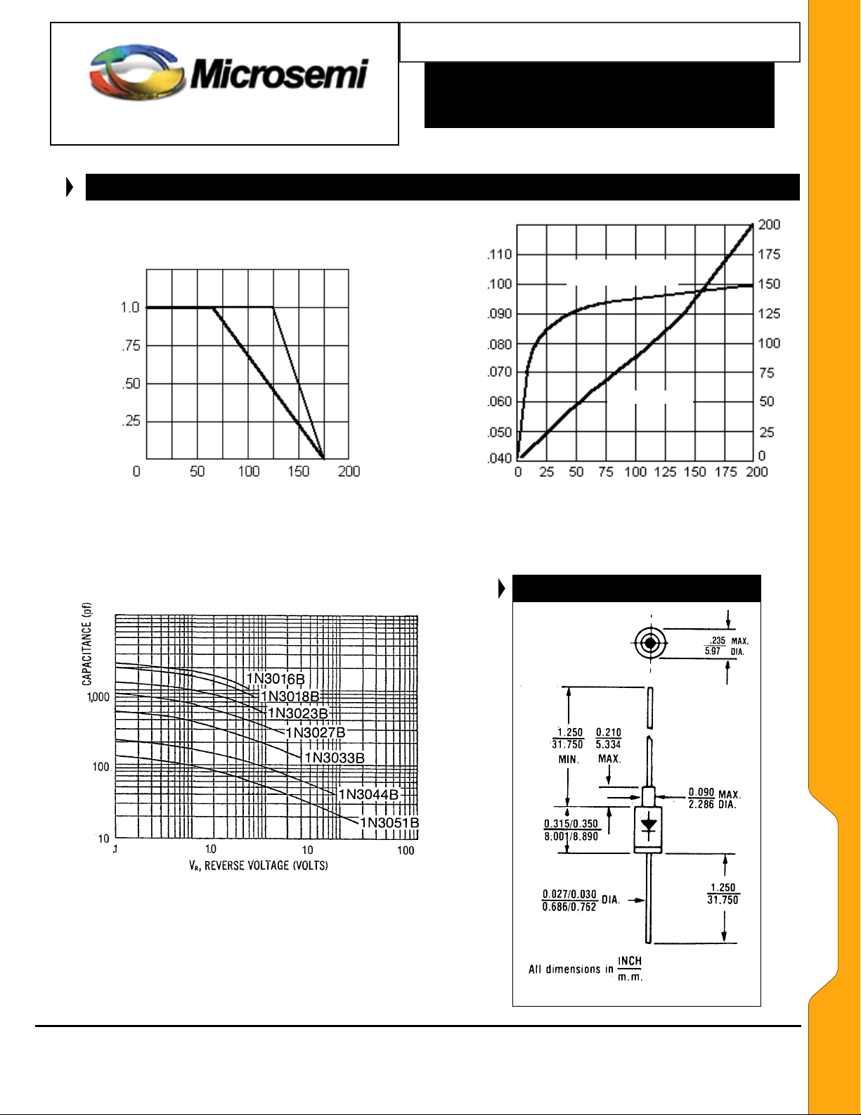
OUTLINE AND CIRCUIT
WWW.
Microsemi
TEMPERATURE COEFFICIENT mV/
WATTS
C
o
Voltage Temperature
Coefficient %/
o
C
. COM
- RATED POWER
d
P
DISSIPATION
TL – Lead Temperature (oC) 3/8” from body
TEMPERATURE COEFFICIENT %/
NOMINAL ZENER VOLTAGE (VOLTS)
mV Change /oC
or TA on FR4 PC Board FIGURE 2
FIGURE 1 Typical Zener Voltage Temperature
Power Derating Curve Coeff. vs. Zener Voltage
PACKAGE DIMENSIONS
o
C
FIGURE 3
Typical Capacitance vs. Reverse Voltage for 1-Watt Zeners
Copyright 2003
11-03-2003 REV A
Microsemi
Scottsdale Division
8700 E. Thomas Rd. PO Box 1390, Scottsdale, AZ 85252 USA, (480) 941-6300, Fax: (480) 947-1503
DO-13 (DO-202AA)
Page 3
1N3016B – 1N3051B
Page 4

WWW.ALLDATASHEET.COM
Copyright © Each Manufacturing Company.
All Datasheets cannot be modified without permission.
This datasheet has been download from :
www.AllDataSheet.com
100% Free DataSheet Search Site.
Free Download.
No Register.
Fast Search System.
www.AllDataSheet.com
 Loading...