

Page 1

Programmable, Isolated
a
FEATURES
Internal Isolated Loop Supply Drives 1000 ⍀ Load
Pin Programmable Inputs: 0 V to +5 V or 0 V to +10 V
Pin Programmable Outputs: 4 to 20 mA or 0 to 20 mA
High CMV Isolation: 1500 V RMS
Normal-Mode Output Protection: 240 V RMS
High Accuracy
Low Offset Tempco: ⴞ300 nA/ⴗC
Low Gain Tempco: ⴞ50 ppm/ⴗC
Low Nonlinearity: ⴞ0.02%
High CMR: 90 dB min
Small Package: 1.0" ⴛ 2.10" ⴛ 0.35"
Meets IEEE STD 472: CMV Transient Protection (SWC)
APPLICATIONS
Multichannel Process Control
D/A Converter—Current Loop Interface
Analog Transmitters and Controllers
Remote Data Acquisition Systems
GENERAL DESCRIPTION
The 1B22 is an isolated voltage-to-current converter that
incorporates transformer isolation to achieve high performance
and automated surface mount manufacturing for low cost
and increased reliability. Designed for industrial applications,
it is especially suited for harsh environments with extremely
high common-mode interference. With programmable inputs
and outputs, the 1B22 provides an unbeatable combination of
versatility and performance in a compact plastic package.
Functionally, the V/I converter consists of four basic sections:
input conditioning, modulator/demodulator, isolated loop
supply and current source (Figure 1). The 1B22 is pin programmable for 0 V to +5 V or 0 V to +10 V inputs and 0 to 20 mA
or 4 to 20 mA outputs using an internal resistor network. It can
also be set by an external resistor to accept 0 V to +1 V to 0 V
to +10 V inputs. Transformer coupling provides 1500 V rms
galvanic isolation between the inputs and the current loop.
Nonlinearity is an excellent ±0.05% max.
Loop power is generated internally through a dc/dc converter
and is also isolated from the input side (1500 V rms). Loop
compliance voltage is dependent on the voltage supplied to the
1B22, and with V
load.
The 1B22 is fully specified over –25°C to +85°C and operates
over the industrial (–40°C to +85°C) temperature range.
= 28 V, it is sufficient to drive a 1000 Ω
LOOP
Voltage-to-Current Converter
1B22
FUNCTIONAL BLOCK DIAGRAM
IN1
IN2
4mA
OFFSET
S. NODE
SYNC
+15V
–15V
A. COM
RESISTOR
NETWORK
REF
OSCILLATOR
V
P. COM
SIGNAL
ISOLATION
POWER
ISOLATION
LOOP
DESIGN FEATURES AND USER BENEFITS
Isolated Loop Power: Internal loop supply completely
isolates the loop from the input terminals (1500 V rms) and
provides the capability to drive 0 Ω to 1000 Ω loads. This eliminates the need for an external dc/dc converter.
Ease of Use: The 1B22 offers complete isolated voltage-tocurrent conversion with minimum external parts required to get
a conditioned current signal. No external buffers or drivers are
required.
High CMV Isolation: The 1B22 features high input to output
galvanic isolation to eliminate ground loops and offer protection
against damage from transients and fault voltages. The isolation
barrier will withstand continuous CMV of 1500 V rms and meets
the IEEE Standard for Common-Mode Voltage Transient Protection (STD 472-SWC).
Small Size: The 1B22 package size (1.0" × 2.1" DIP) makes it
an excellent choice in multichannel systems for maximum channel density. The 0.35" height also facilitates applications with
limited board clearance.
1B22
DEMODULATORMODULATOR
RECTIFIER/
LOOP SUPPLY
PROT
OUT
HI
OUT
LO
REV. B
Information furnished by Analog Devices is believed to be accurate and
reliable. However, no responsibility is assumed by Analog Devices for its
use, nor for any infringements of patents or other rights of third parties
which may result from its use. No license is granted by implication or
otherwise under any patent or patent rights of Analog Devices.
One Technology Way, P.O. Box 9106, Norwood, MA 02062-9106, U.S.A.
Tel: 781/329-4700 World Wide Web Site: http://www.analog.com
Fax: 781/326-8703 © Analog Devices, Inc., 2000
Page 2
1B22–SPECIFICATIONS
(typical @ +25ⴗC and VS = ⴞ15 V, V
= +24 V, unless otherwise noted)
LOOP
Model 1B22AN
INPUT SPECIFICATIONS
Factory Calibrated, User Selectable 0 V to +5 V, 0 V to +10 V
Input Impedance
0 V to +10 V Input Range 50 kΩ
0 V to +5 V Input Range 25 kΩ
OUTPUT SPECIFICATIONS
Current Output Range, User Selectable 4 to 20 mA, 0 to 20 mA
Load Compliance Range, V
Load Compliance Range, V
= +15 V 8 V min
LOOP
= +28 V 20 V min
LOOP
Maximum Output Current @ Input Overload 30 mA
Output Noise, 100 Hz Bandwidth 300 nA p-p
NONLINEARITY (% of Span) ± 0.02% (± 0.05% max)
ISOLATION
CMV, Input to Output Continuous 1500 V rms max
CMR, @ 60 Hz 90 dB min
Normal-Mode Output Protection 240 V rms Continuous
CMV Transient Protection IEEE-STD 472 (SWC)
ACCURACY
Warm-Up Time to Rated Performance 5 min
Total Output Error @ +25°C
Offset (V
Span (V
= 0 V) ± 60 µA
IN
= +10 V) ± 0.7% Full Scale
IN
vs. Temperature (–25°C to +85°C)
Offset ± 300 nA/°C
Span ± 50 ppm/°C
DYNAMIC RESPONSE
Settling Time to 0.1% of FS for 10 V Step 9 ms
Small Signal Bandwidth 400 Hz
POWER SUPPLY
Bipolar Input Supplies
Operating Voltage ± 15 V ± 5%
Quiescent Current ± 7.5 mA
Power Supply Rejection ± 0.01%/V
Loop Supply
Operating Voltage +14 V to +30 V
Operating Current, at Full-Scale Output 25 mA
Loop Supply Rejection ± 0.005%/V
ENVIRONMENTAL
Temperature Range
Rated Performance –25°C to +85°C
Operating –40°C to +85°C
Storage –40°C to +85°C
Relative Humidity, Noncondensing 0 to 95% @ 60°C
CASE SIZE 1.0" × 2.1" × 0.35"
Specifications subject to change without notice.
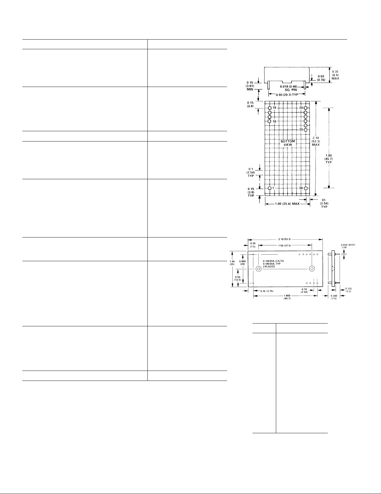
OUTLINE DIMENSIONS
Dimensions shown in inches and (mm).
AC1225 MATING SOCKET
PIN DESIGNATIONS
Pin Function
11 OUT HI
16 IN2
17 IN1
18 S. NODE
19 4 mA OFFSET
20 +15 V
21 ANA COM
22 –15 V
23 SYNC
24 V
LOOP
25 POWER COM
38 OUT LO
–2–
REV. B
Page 3

INSIDE THE 1B22
The 1B22 produces an isolated 4 to 20 mA or 0 to 20 mA output current which is proportional to the input voltage and
independent of the output load resistance (Figure 1). The input
stage is configured as an inverting amplifier with a resistor network to provide pin-strappable input ranges of 0 V to +5 V and
0 V to +10 V and output ranges of 0 to 20 mA and 4 to 20 mA.
The conditioned signal is modulated to generate a square wave
that drives transformer T1. The peak-to-peak amplitude of the
signal is proportional to V
. An internal, high stability reference
IN
with a nominal output voltage of +6.4 V is used to develop a
4 mA offset for the 4 to 20 mA current loop output.
1B22
Figure 2. Basic Interconnections
Figure 1. 1B22 Functional Block Diagram
After passing through signal transformer T1, the amplitude
modulated signal is demodulated and filtered by a single pole
filter. This filtered output is the control signal for the voltageto-current converter stage. Timing information for the
demodulator is derived from the power transformer T2. The
1B22 outputs are protected from accidental shorts to ac line
voltages up to 240 V rms. Combined with 1500 V input to output isolation, the 1B22 provides unbeatable protection against
transients, wiring errors and current loop short circuits to power
lines.
The dc-dc converter consists of a power driver, power transformer T2, a full wave rectifier and a filter. The dc-dc converter
provides the power for the output circuitry as well as the
isolated compliance voltage for the loop. This voltage is proportional to V
on the input side. The 1B22 requires ±15 V
LOOP
supplies to power the input side circuitry and a +14 V to +30 V
supply for the dc-dc converter.
USING THE 1B22
Basic Interconnections: The 1B22 may be applied to achieve
rated performance as shown in Figure 2. For 0 V to 10 V signals
either IN1 or IN2 can be used for input; for 0 V to +5 V signals
jumper IN1 to IN2. Similarly, for 4 to 20 mA operation the
4 mA OFFSET node should be jumpered to the S. NODE,
while for 0 to 20 mA it should be tied to COM. Figure 3 shows
the functional diagram of the resistor network used in the 1B22.
For applications where a separate loop supply is not available,
the ± 15 V supplies can be used by connecting +15 V to V
LOOP
(Pin 24) and COM to P.COM (Pin 25). For additional compliance voltage, P.COM can be connected to –15 V to drive higher
loads.
Figure 3. Internal Resistor Network
Optional Trim Adjustments: Figure 4 is an example of using
potentiometers for trimming gain and offset for a 0 V to +10 V
input and 4 to 20 mA output. The network for offset adjustment
keeps the resistors relatively small to minimize noise effects
while giving a sensitivity of ±1% of span. The value of R1
should be 5 MΩ for the 0 V to +10 V range (for 0 V to +5 V
configurations, a 1.2 MΩ resistor should be used). For more
adjustment range, resistors smaller than 274 kΩ can be used.
50k⍀
+15V
–15V
V
IN
274k⍀
1k⍀
1k⍀
20k⍀
R1
SYNC
+15V
COM
–15V
IN1
IN2
4mA
OFF
S. NODE
50k⍀
RESISTOR
NETWORK
POWER
DRIVER
V
LOOP
P. COM
1B22
REF
RECTIFIER/
LOOP
SUPPLY
PROT
OUT
HI
OUT
LO
Figure 4. Optional Offset and Span Adjustment
REV. B
–3–
Page 4

1B22
Synchronizing Multiple 1B22s: In applications where multiple 1B22s are used in close proximity, radiated individual
oscillator frequencies may cause “beat frequency” related output errors. These errors can be eliminated by driving the SYNC
pins of all the units with a 40 kHz clock circuit at 50% duty
cycle (Figure 5). The SYNC input typically has an input impedance of 150 kΩ储180 pF.
Figure 5. Multiple 1B22s’ Synchronization
Loop Supply Requirements: The 1B22 design allows flexible
loop supply options. The loop supply voltage required for any
value of load resistance can be calculated from the following
equation:
2R
+ 780
V
LOOP
L
=
106
This value allows for approximately 10% overrange capability.
The graph in Figure 6 shows the relationship between supply
voltage and load resistance.
APPLICATIONS
Isolated D/A Converter: The 1B22 offers total ground isola-
tion and protection from high voltage transients in interfacing
D/A converters to standard 4 to 20 mA current loops. The D/A
converter, such as the Analog Devices’ 12-bit AD7245
DACPORT®, should be connected for operation on the unipolar 0 V to +10 V output range. This is shown in Figure 7.
C1193a–2.2–3/00 (rev. B)
Figure 7. D/A Converter–Isolated 4-20 mA Interface
Pressure Transmitter: In Figure 8, the 1B22 is used in a
pressure transmitter application to provide complete inputoutput isolation and avoid signal errors due to ground loop currents. The process pressure is monitored with a strain gage type
pressure transducer interfaced by the Analog Devices’ 1B32
transducer signal conditioner. The high level voltage output of
the 1B32 is converted to the isolated 4 to 20 mA current for
transmission to a remote recorder or indicator.
Figure 6. Loop Supply vs. Load
Figure 8. Isolated Pressure Transmitter
DACPORT is a registered trademark of Analog Devices, Inc.
–4–
PRINTED IN U.S.A.
REV. B
 Loading...