

Page 1
1.5KE6V8A/440A
®
FEATURES
PEAK PULSE POWER : 1500 W (10/1000µs)
■
BREAKDOWN VOLTAGE RANGE :
■
From 6.8V to 440 V
UNI AND BIDIRECTIONAL TYPES
■
LOW CLAMPING FACTOR
■
FAST RESPONSE TIME
■
UL RECOGNIZED
■
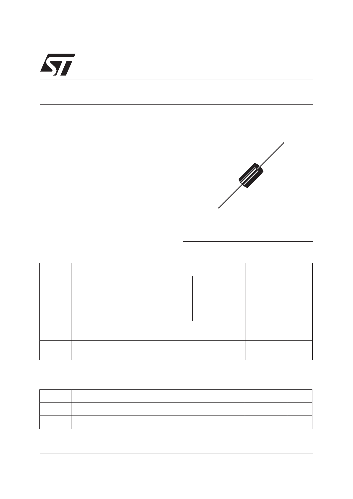
DESCRIPTION
Transil diodes provide high overvoltage protection
by clampingaction. Their instantaneous response
to transient overvoltages makes them particularly
suited to protect voltage sensitive devices such
as MOS Technology and low voltage supplied
IC’s.
1.5KE6V8CA/440CA
TRANSIL
DO-201
TM
ABSOLUTE MAXIMUM RATINGS (T
amb
= 25°C)
Symbol Parameter Value Unit
P
PP
P
I
FSM
T
stg
T
j
T
L
Peak pulse power dissipation (see note 1) Tj initial = T
Power dissipation on infinite heatsink T
Non repetitive surge peak forward current
for unidirectional types
= 75°C
amb
tp = 10ms
Tj initial = T
Storage temperature range
Maximum junction temperature
Maximum lead temperature for soldering during 10s at 5mm
amb
amb
1500 W
5W
200 A
-65to+175
175
230 °C
from case
Note 1 :For a surge greater than the maximum values, the diode will fail in short-circuit.
THERMAL RESISTANCES
Symbol Parameter Value Unit
R
R
th (j-l)
th (j-a)
Junction to leads
Junction to ambient on printed circuit. L
lead
=10mm
20 °C/W
75 °C/W
°C
°C
February 2002- Ed: 3A
1/6
Page 2
1.5KExx
ELECTRICAL CHARACTERISTICS (T
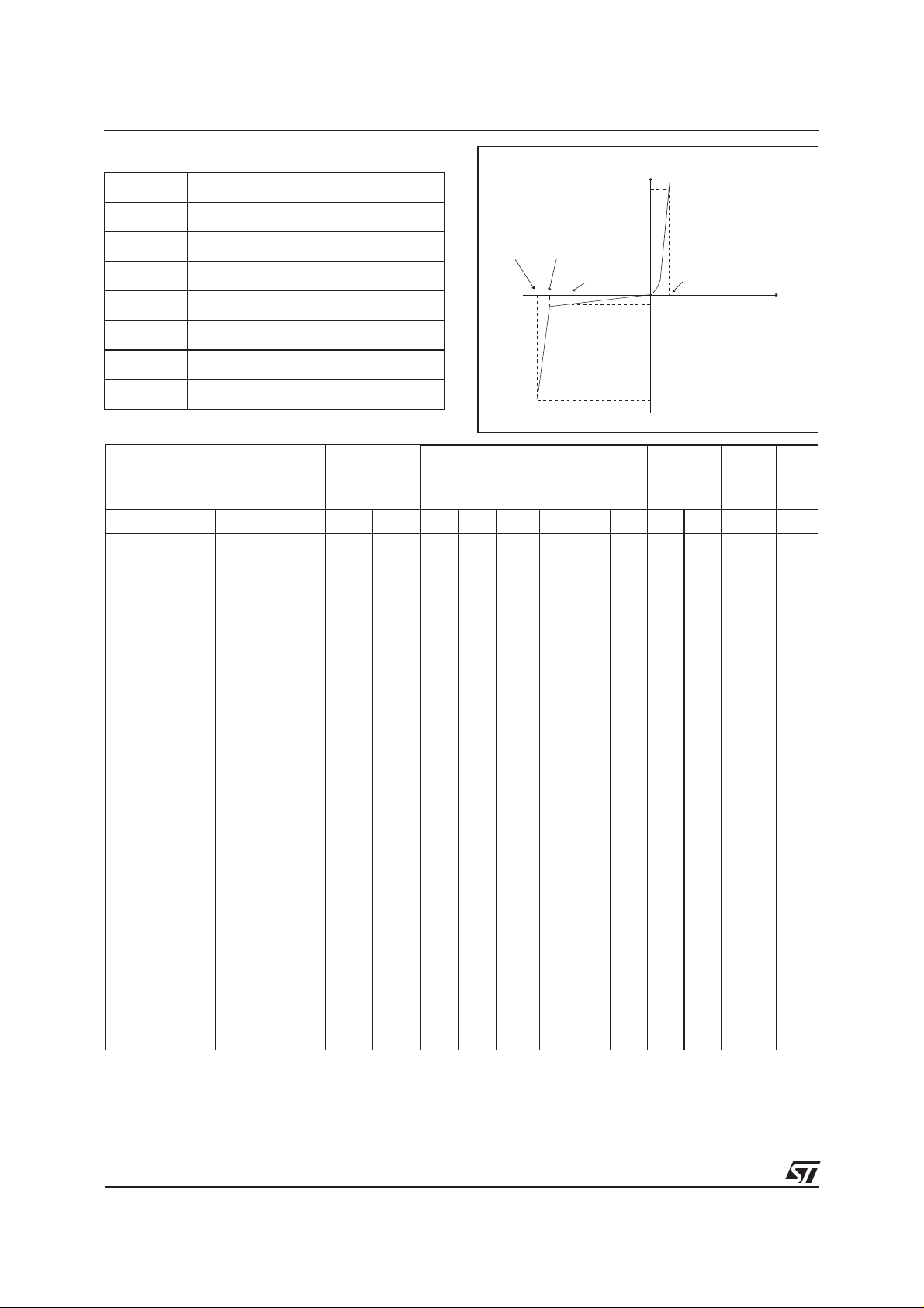
Symbol Parameter
V
V
V
I
I
αT
RM
PP
V
RM
BR
CL
F
Stand-off voltage
Breakdown voltage
Clamping voltage
Leakage current @ V
Peak pulse current
Voltage temperature coefficient
Forward voltage drop
Types IRM@V
RM
amb
= 25°C)
RM
I
I
F
VV
CLVBR
V
RM
I
I
RM
PP
V
F
VBR@IRVCL@IPPVCL@I
PP
max min nom max max max max typ
note2 10/1000µs 8/20µs note3 note4
Unidirectional Bidirectional µA V VV VmAVAVA10
1.5KE6V8A 1.5KE6V8CA 1000
1.5KE7V5A 1.5KE7V5CA 500
1.5KE10A 1.5KE10CA 10
1.5KE12A 1.5KE12CA 5
1.5KE15A 1.5KE15CA 1
1.5KE18A 1.5KE18CA 1
1.5KE22A 1.5KE22CA 1
1.5KE24A 1.5KE24CA 1
1.5KE27A 1.5KE27CA 1
1.5KE30A 1.5KE30CA 1
1.5KE33A 1.5KE33CA 1
1.5KE36A 1.5KE36CA 1
1.5KE39A 1.5KE39CA 1
1.5KE47A 1.5KE47CA 1
1.5KE56A 1.5KE56CA 1
1.5KE62A 1.5KE62CA 1
1.5KE68A 1.5KE68CA 1
1.5KE82A 1.5KE82CA 1
1.5KE100A 1.5KE100CA 1
1.5KE120A 1.5KE120CA 1
1.5KE150A 1.5KE150CA 1
1.5KE180A 1.5KE180CA 1
5.8 6.45 6.8 7.14 10 10.5 143 13.4 746 5.7 9500
6.4 7.13 7.5 7.88 10 11.3 132 14.5 690 6.1 8500
8.55 9.5 10 10.5 1 14.5 100 18.6 538 7.3 7000
10.2 11.4 12 12.6 1 16.7 90 21.7 461 7.8 6000
12.8 14.3 15 15.8 1 21.2 71 27.2 368 8.4 5000
15.3 17.1 18 18.9 1 25.2 59.5 32.5 308 8.8 4300
18.8 20.9 22 23.1 1 30.6 49 39.3 254 9.2 3700
20.5 22.8 24 25.2 1 33.2 45 42.8 234 9.4 3500
23.1 25.7 27 28.4 1 37.5 40 48.3 207 9.6 3200
25.6 28.5 30 31.5 1 41.5 36 53.5 187 9.7 2900
28.2 31.4 33 34.7 1 45.7 33 59.0 169 9.8 2700
30.8 34.2 36 37.8 1 49.9 30 64.3 156 9.9 2500
33.3 37.1 39 41.0 1 53.9 28 69.7 143 10.0 2400
40.2 44.7 47 49.4 1 64.8 23.2 84 119 10.1 2050
47.8 53.2 56 58.8 1 77 19.5 100 100 10.3 1800
53.0 58.9 62 65.1 1 85 17.7 111 90 10.4 1700
58.1 64.6 68 71.4 1 92 16.3 121 83 10.4 1550
70.1 77.9 82 86.1 1 113 13.3 146 69 10.5 1350
85.5 95.0 100 105 1 137 11 178 56 10.6 1150
102 114 120 126 1 165 9.1 212 47 10.7 1000
128 143 150 158 1 207 7.2 265 38 10.8 850
154 171 180 189 1 246 6.1 317 31.5 10.8 725
V
αTC
-4
/°C pF
2/6
Page 3
1.5KExx
Types I
RM@VRM
VBR@IRVCL@IPPVCL@I
αTC
PP
max min nom max max max max typ
note2 10/1000µs 8/20µs note3 note4
Unidirectional Bidirectional µA V VV VmAVAVA10
1.5KE200A 1.5KE200CA 1
1.5KE220A 1.5KE220CA 1
1.5KE250A 1.5KE250CA 1
1.5KE300A 1.5KE300CA 1
1.5KE350A 1.5KE350CA 1
1.5KE400A 1.5KE400CA 1
1.5KE440A 1.5KE440CA 1
171 190 200 210 1 274 5.5 353 28 10.8 675
188 209 220 231 1 328 4.6 388 26 10.8 625
213 237 250 263 1 344 5.0 442 23 11 560
256 285 300 315 1 414 5.0 529 19 11 500
299 332 350 368 1 482 4.0 618 16 11 430
342 380 400 420 1 548 4.0 706 14 11 390
376 418 440 462 1 603 3.5 776 13 11 360
-4
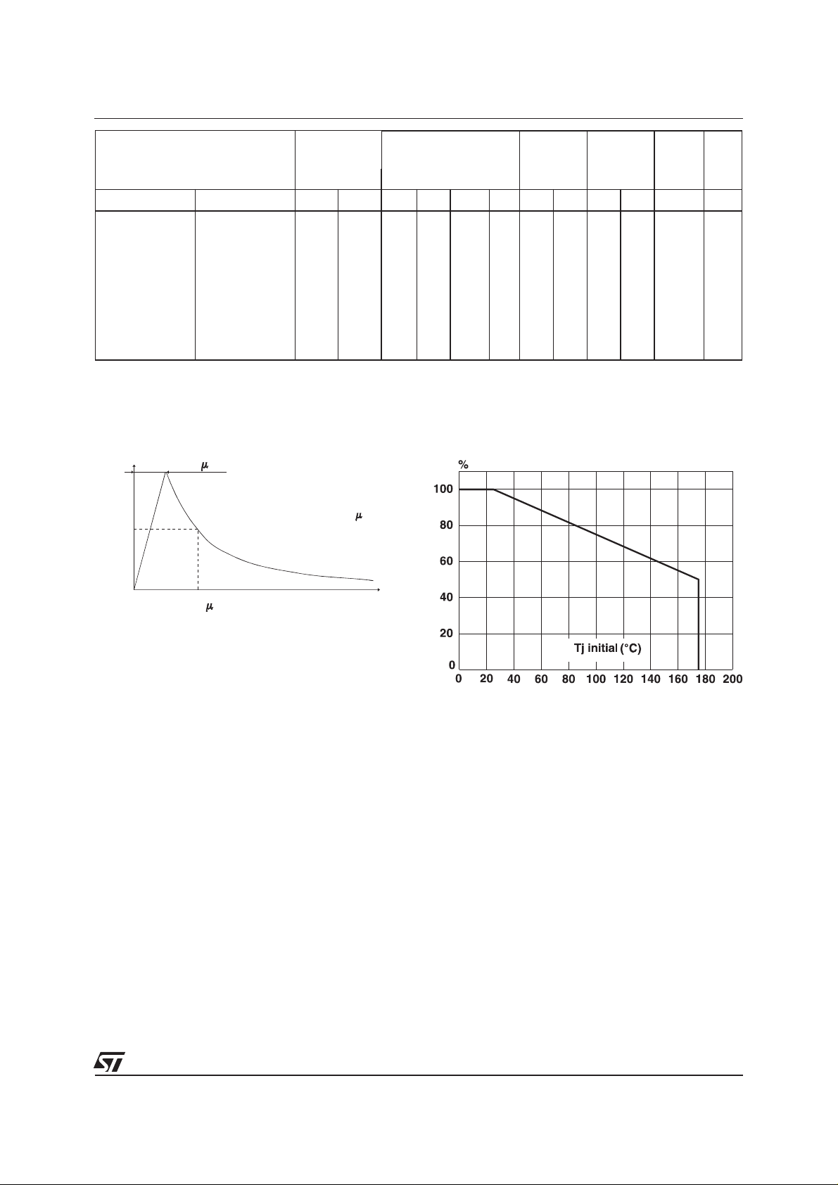
Fig. 1: Peak pulse power dissipation versus
%I
100
50
PP
10 s
PULSE WAVEFORM 10/1000 s
initial junction temperature (printed circuit
/°C pF
0
1000 s
Note 2 : Pulsetest: tp<50ms.
Note 3 : ∆VBR= αT*(T
Note 4 : VR= 0 V, F = 1 MHz. For bidirectional types,
capacitance value is divided by 2.
- 25)*VBR(25°C).
amb
t
3/6
Page 4
1.5KExx
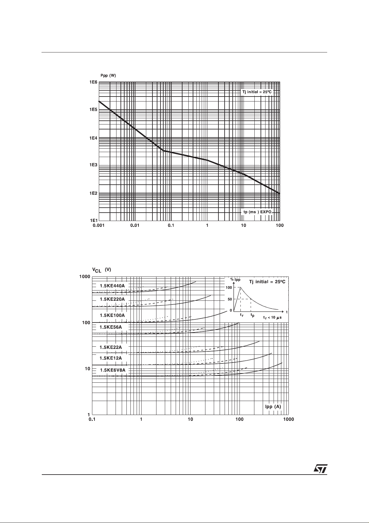
Fig. 2 : Peak pulse power versus exponential pulse duration.
Fig. 3 : Clampingvoltage versus peak pulse current.
Exponential waveform: t
=20µs________
p
= 1ms——————-
t
p
= 10 ms ...............
t
p
Note : The curves of the figure 3 are specified for a junction temperature of 25°C before surge.
The given results may be extrapolated for other junction temperatures by using the following formula :
∆V
= αT* (T
BR
-25) * VBR(25°C).
amb
For intermediate voltages, extrapolate the given results.
4/6
Page 5
1.5KExx
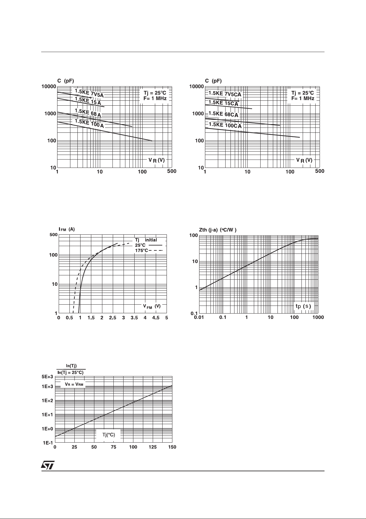
Fig. 4a : Capacitance versus reverse applied
voltage for unidirectional types (typical values).
Fig. 5 : Peak forward voltage drop versus peak
forward current (typical values for unidirectional
types).
Note : Multiply by 2 for units with VBR> 220 V.
Fig. 4b : Capacitance versus reverse applied
voltage for bidirectional types (typical values).
Fig. 6 : Transient thermal impedance junction-ambient versus pulse duration (For FR4 PC
Board with L
= 10mm).
lead
Fig. 7 : Relative variation of leakage current
versus junction temperature.
5/6
Page 6
1.5KExx
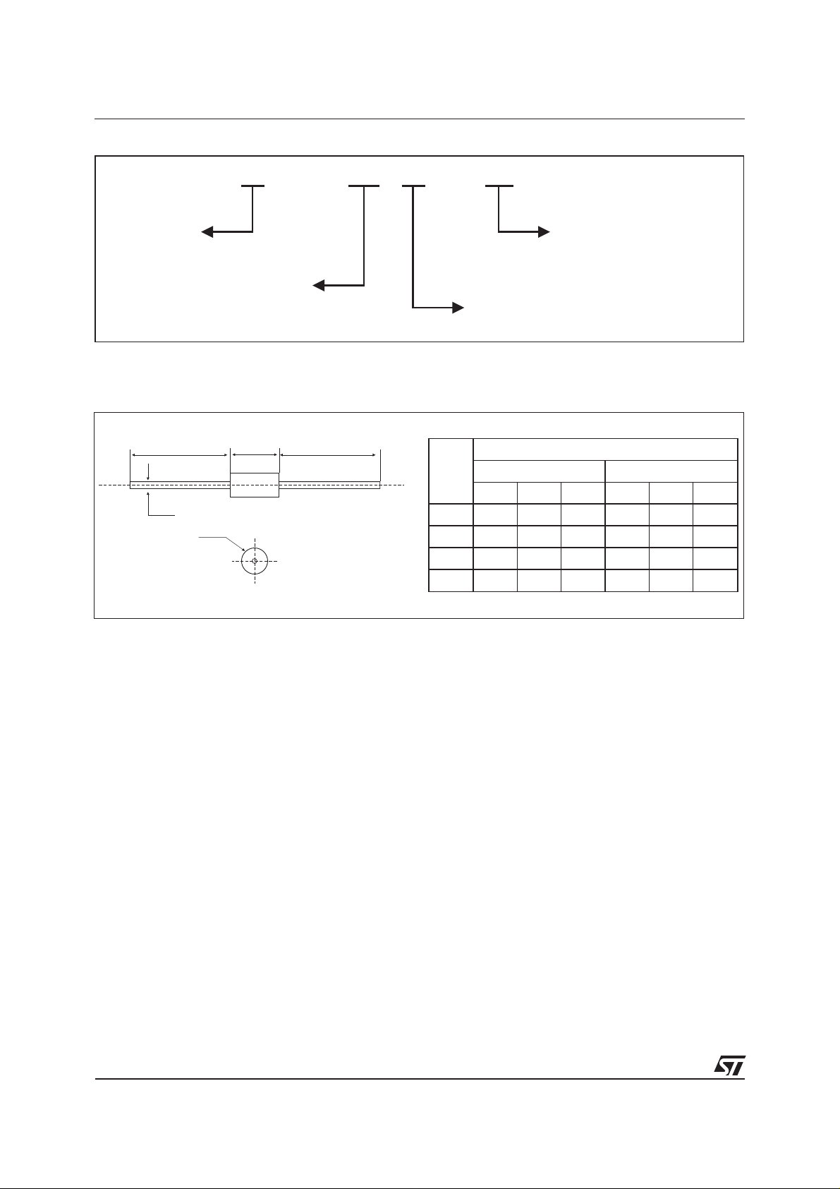
ORDER CODE
1.5 KE 100 C A RL
1500W
PACKAGING
= Ammopack tape
RL = Tape & reel
BREAKDOWNVOLTAGE
BIDIRECTIONAL
No suffix: Unidirectional
MARKING : Logo, Date Code, Type Code, Cathode Band (for unidirectional types only).
PACKAGE MECHANICAL DATA
DO-201 (Plastic)
B
∅D
∅C
AB
DIMENSIONS
REF.
Millimeters Inches
Min. Typ. Max. Min. Typ. Max.
A 8.5 9.5 0.335 0.374
B 25.4 1
∅ C 4.8 5.3 0.189 0.209
∅ D 0.96 1.06 0.038 0.042
Packaging : standard packaging is in tape and reel.
Weight = 0.876 g.
Informationfurnished is believed to be accurate and reliable. However, STMicroelectronics assumes no responsibility for the consequences of
useof such information nor for any infringement of patents or other rights of third parties which may result from its use. No license is granted by
implication or otherwise under any patent or patent rights of STMicroelectronics. Specifications mentioned in this publication are subject to
change without notice. This publication supersedes and replaces all information previously supplied.
STMicroelectronics products are not authorized for use as critical components in life support devices or systems without express written
approval of STMicroelectronics.
The ST logo is a registered trademark of STMicroelectronics
© 2003 STMicroelectronics - Printed in Italy - All rights reserved.
STMicroelectronics GROUP OF COMPANIES
Australia - Brazil - Canada - China - Finland - France - Germany
Hong Kong - India - Israel - Italy - Japan - Malaysia - Malta - Morocco - Singapore
Spain - Sweden - Switzerland - United Kingdom - United States.
http://www.st.com
6/6
 Loading...