

Page 1
184PIN DDR266 Unbuffered DIMM
E
6
V
4
6
D
L
M
8
2
1
S
T
T
T
S
S
1
1
2
2
8
8
M
M
L
L
D
D
6
6
4
4
V
V
6
6
E
E
1GB With 64Mx4 CL2.5
Description
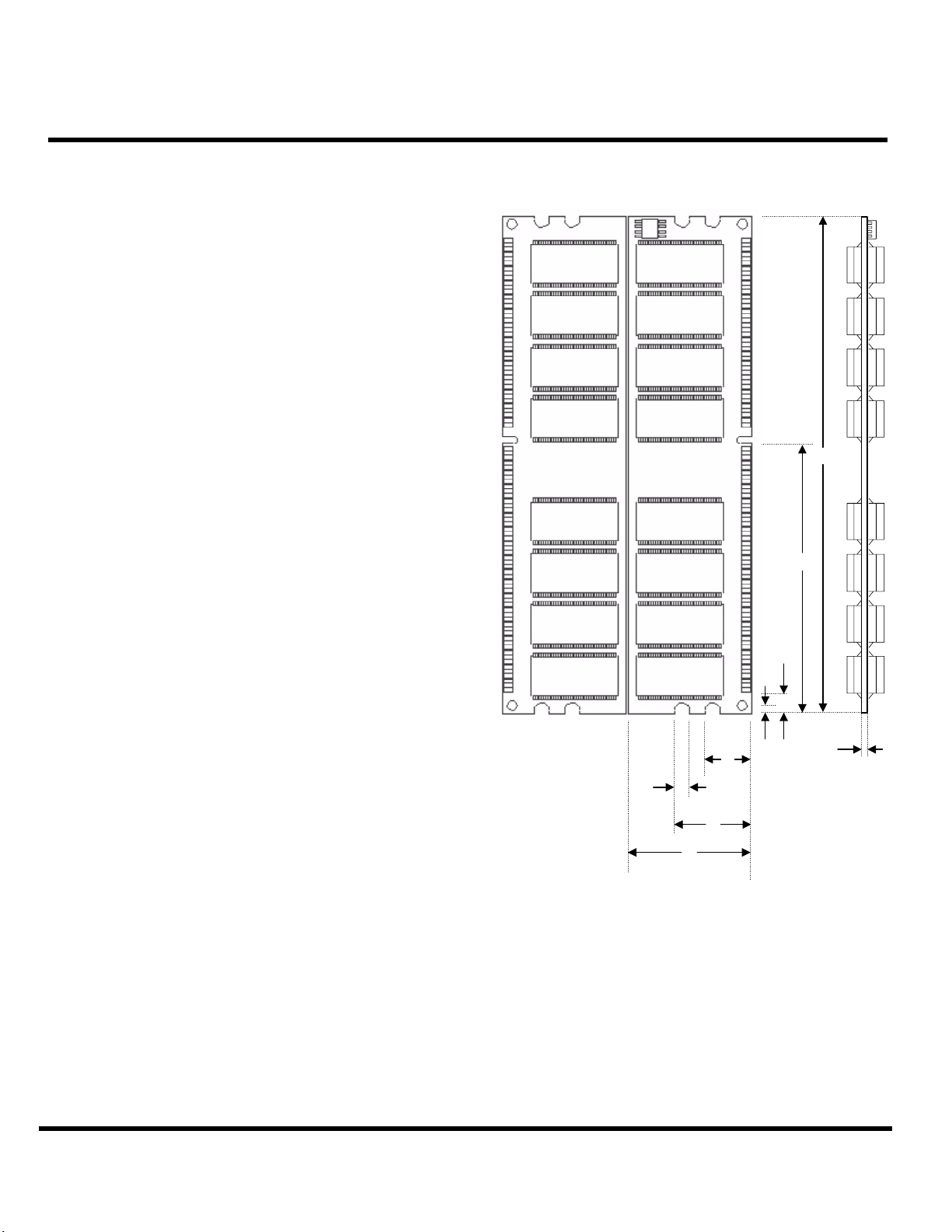
The TS128MLD64V6E is a 128Mx64bits Double Data
Rate SDRAM high density for DDR266. The
TS128MLD64V6E consists of 32pcs CMOS 64Mx4 bits
Double Data Rate SDRAMs in 66 pin TSOP-II 400mil
packages and a 2048 bits serial EEPROM on a 184-pin
printed circuit board. The TS128MLD64V6E is a Dual
In-Line Memory Module and is intended for mounting into
184-pin edge connector sockets.
Synchronous design allows precise cycle control with the
use of system clock. Data I/O transactions are possible
on both edges of DQS. Range of operation frequencies,
programmable latencies allow the same device to be
useful for a variety of high bandwidth, high performance
memory system applications.
Features
• Power supply: VDD: 2.5V ± 0.2V
Placement
A
B
VDDQ: 2.5V ± 0.2V
• Max clock Freq: 133MHZ.
• Double-data-rate architecture; two data transfers per
clock cycle
• Differential clock inputs (CK and /CK)
• DLL aligns DQ and DQS transition with CK transition
• Auto and Self Refresh 7.8us refresh interval.
• Data I/O transactions on both edge of data strobe.
• Edge aligned data output, center aligned data
• Serial Presence Detect (SPD) with serial EEPROM
• SSTL-2 compatible inputs and outputs.
• MRS cycle with address key programs.
CAS Latency (Access from column address): 2.5
Burst Length (2, 4, 8)
Data Sequence (Sequential & Interleave)
H
G
F
E
PCB: 09-1670
C
D
I
Transcend Information Inc.
1
Page 2
184PIN DDR266 Unbuffered DIMM
E
6
V
4
6
D
L
M
8
2
1
S
T
T
T
S
S
1
1
2
2
8
8
M
M
L
L
D
D
6
6
4
4
V
V
6
6
E
E
1GB With 64Mx4 CL2.5
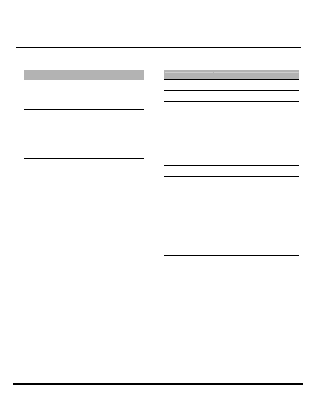
Dimensions
Side Millimeters Inches
A 133.35±0.20 5.250±0.008
B 72.39 2.850
C 6.35 0.250000
D 2.20 0.0870
E 31.75±0.20 1.250±0.00800
F 19.80 0.780
G 4.00 0.157
H 12.00 0.472
I 1.27±0.10 0.050±0.004
(Refer Placement)
Pin Identification
Symbol Function
A0~A12, BA0, BA1 Address input
DQ0~DQ63 Data Input / Output.
DQS0~DQS7 Data strobe input/output
CK0, /CK0,
CK1, /CK1,
CK2, /CK2
CKE0, CKE1 Clock Enable Input.
/CS0, /CS1 Chip Select Input.
/RAS Row Address Strobe
/CAS Column Address Strobe
/WE Write Enable
DM0~DM7 Data-in Mask
VDD +2.5 Voltage power supply
Clock Input.
VDDQ +2.5 Voltage Power Supply for DQS
VREF Power Supply for Reference
+2.5 Voltage Serial EEPROM
VDDSPD
SA0~SA2 Address in EEPROM
SCL Serial PD Clock
SDA Serial PD Add/Data input/output
VSS Ground
NC No Connection
Power Supply
Transcend Information Inc.
2
Page 3
S
T
S
T
S
T
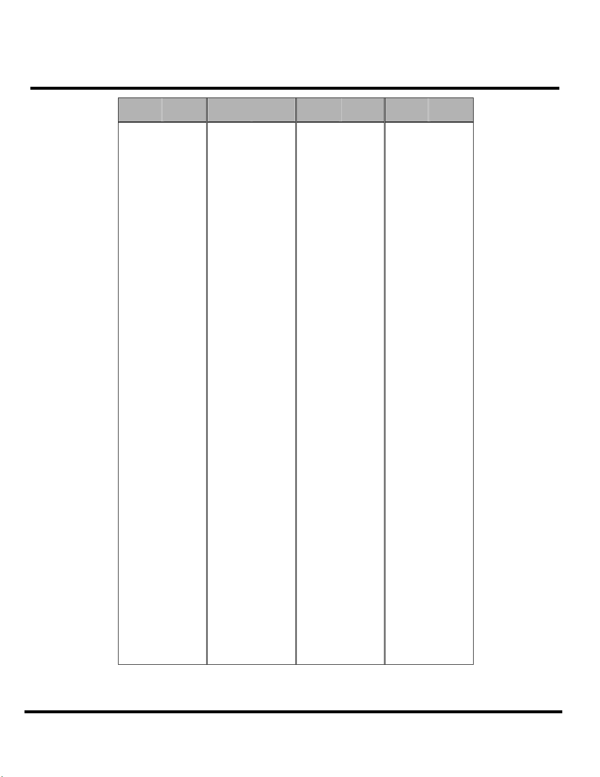
Pinouts:
1
1
1
2
2
2
8
8
8
M
M
D
L
D
L
Pin
No
01 VREF 47 *DQS8 93 VSS 139 VSS
02 DQ0 48 A0 94 DQ4 140 *DM8
03 VSS 49 *CB2 95 DQ5 141 A10
04 DQ1 50 VSS 96 VDDQ 142 *CB6
05 DQS0 51 *CB3 97 DM0 143 VDDQ
06 DQ2 52 BA1 98 DQ6 144 *CB7
07 VDD 53 DQ32 99 DQ7 145 VSS
08 DQ3 54 VDDQ 100 VSS 146 DQ36
09 NC 55 DQ33 101 NC 147 DQ37
10 NC 56 DQS4 102 NC 148 VDD
11 VSS 57 DQ34 103 NC 149 DM4
12 DQ8 58 VSS 104 VDDQ 150 DQ38
13 DQ9 59 BA0 105 DQ12 151 DQ39
14 DQS1 60 DQ35 106 DQ13 152 VSS
15 VDDQ 61 DQ40 107 DM1 153 DQ44
16 *CK1 62 VDDQ 108 VDD 154 /RAS
17 */CK1 63 /WE 109 DQ14 155 DQ45
18 VSS 64 DQ41 110 DQ15 156 VDDQ
19 DQ10 65 /CAS 111 *CKE1 157 /CS0
20 DQ11 66 VSS 112 VDDQ 158 */CS1
21 CKE0 67 DQS5 113 NC 159 DM5
22 VDDQ 68 DQ42 114 DQ20 160 VSS
23 DQ16 69 DQ43 115 *A12 161 DQ46
24 DQ17 70 VDD 116 VSS 162 DQ47
25 DQS2 71 NC 117 DQ21 163 NC
26 VSS 72 DQ48 118 A11 164 VDDQ
27 A9 73 DQ49 119 DM2 165 DQ52
28 DQ18 74 VSS 120 VDD 166 DQ53
29 A7 75 */CK2 121 DQ22 167 NC
30 VDDQ 76 *CK2 122 A8 168 VDD
31 DQ19 77 VDDQ 123 DQ23 169 DM6
32 A5 78 DQS6 124 VSS 170 DQ54
33 DQ24 79 DQ50 125 A6 171 DQ55
34 VSS 80 DQ51 126 DQ28 172 VDDQ
35 DQ25 81 VSS 127 DQ29 173 NC
36 DQS3 82 NC 128 VDDQ 174 DQ60
37 A4 83 DQ56 129 DM3 175 DQ61
38 VDD 84 DQ57 130 A3 176 VSS
39 DQ26 85 VDD 131 DQ30 177 DM7
40 DQ27 86 DQS7 132 VSS 178 DQ62
41 A2 87 DQ58 133 DQ31 179 DQ63
42 VSS 88 DQ59 134 *CB4 180 VDDQ
43 A1 89 VSS 135 *CB5 181 SA0
44 *CB0 90 NC 136 VDDQ 182 SA1
45 *CB1 91 SDA 137 CK0 183 SA2
46 VDD 92 SCL 138 /CK0 184 VDDSPD
* Please refer Block Diagram
6
6
V
4
V
4
Pin
Name
V
4
6
D
L
M
6
6
6
E
E
E
Pin
No
Pin
Name
Pin
No
184PIN DDR266 Unbuffered DIMM
1GB With 64Mx4 CL2.5
Pin
Name
Pin
No
Pin
Name
Transcend Information Inc.
3
Page 4
T
T
T
S
S
1
1
2
2
8
8
8
2
1
S
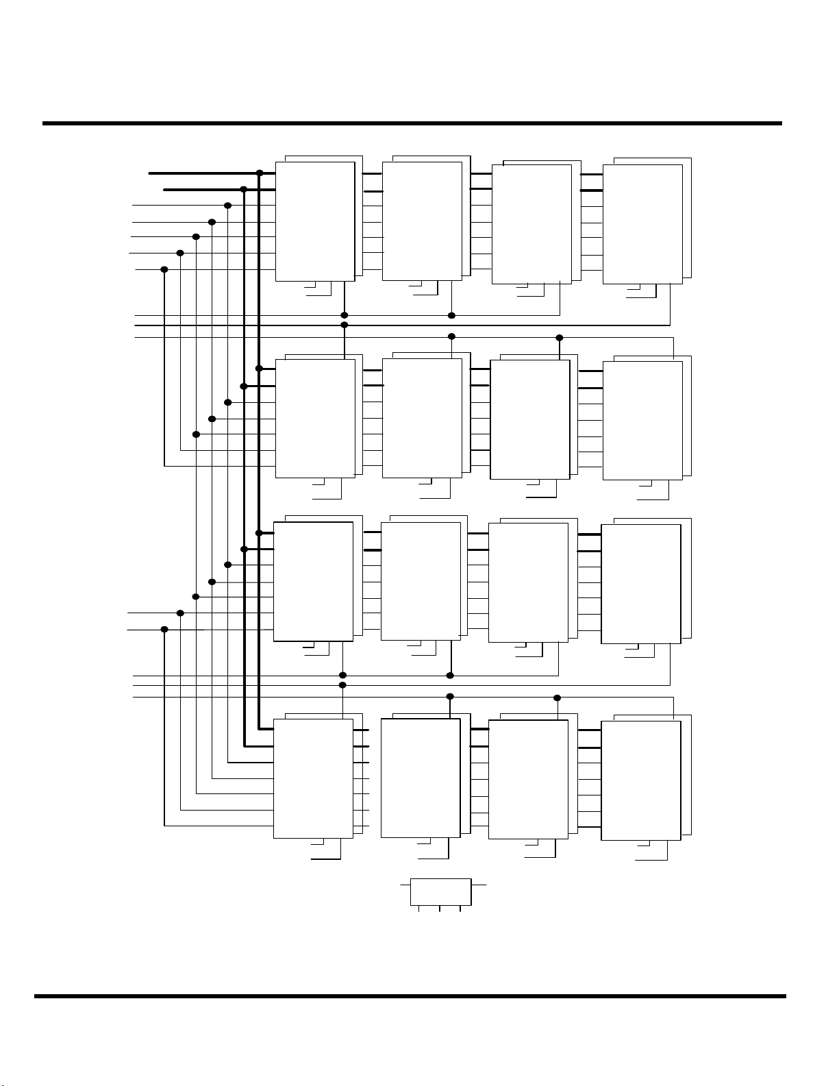
Block Diagram
A0~A12,
BA0,BA1
DQ0~DQ63
/RAS
/CAS
/WE
/CS0
CKE0
CK1,/CK1
CK0,/CK0
CK2,/CK2
M
M
M
L
L
L
D
D
D
6
6
6
4
4
4
V
V
V
E
6
E
6
E
6
A0~A12,
BA0,BA1
DQ0~DQ7
/RAS
/CAS
/WE
/CS
CKE
DM0
DQS0
64MX4
DDR
SDRAM
DM
DQS
CK,/CK
A0~A12,
BA0,BA1
DQ0~DQ7
/RAS
/CAS
/WE
/CS
CKE
DM1
DQS1
64MX4
DDR
SDRAM
DM
DQS
CK,/CK
184PIN DDR266 Unbuffered DIMM
1GB With 64Mx4 CL2.5
A0~A12,
BA0,BA1
DQ0~DQ7
/RAS
/CAS
/WE
/CS
CKE
DM2
DQS2
64MX4
DDR
SDRAM
DM
DQS
CK,/CK
A0~A12,
BA0,BA1
DQ0~DQ7
/RAS
/CAS
/WE
/CS
CKE
DM3
DQS3
64MX4
DDR
SDRAM
DM
DQS
CK,/CK
A0~A12,
BA0,BA1
DQ0~DQ7
/RAS
64MX4
DDR
/CAS
SDRAM
/WE
/CS
64MX4
DDR
SDRAM
DM
64MX4
DDR
SDRAM
DM
DQS
DM
CKE
DM4
DQS4
A0~A12,
BA0,BA1
DQ0~DQ7
/RAS
/CAS
/WE
/CS1
CKE1
CK1,/CK1
CK0,/CK0
CK2,/CK2
This technical information is based on industry standard data and tests believed to be reliable. However, Transcend makes no warranties, either
expressed or implied, as to its accuracy and assume no liability in connection with the use of this product. Transcend reserves the right to make changes
in specifications at any time without prior notice.
/CS
CKE
DM0
DQS0
A0~A12,
BA0,BA1
DQ0~DQ7
/RAS
/CAS
/WE
/CS
CKE
DM4
DQS4
A0~A12,
BA0,BA1
DQ0~DQ7
CK,/CK
/RAS
64MX4
DDR
/CAS
SDRAM
/WE
/CS
DQS
CKE
DM5
DQS5
A0~A12,
BA0,BA1
DQ0~DQ7
/RAS
64MX4
DDR
/CAS
SDRAM
/WE
/CS
CKE
A0~A12,
BA0,BA1
DQ0~DQ7
/RAS
/CAS
/WE
DM5
DQS5
Serial EEPROM
SCL
A0 A1 A2
SA0 SA1 SA2
DM
64MX4
DDR
SDRAM
CK,/CK
DM1
DQS1
CK,/CK
/CS
CKE
DQS
SCL SDA
DM
DQS
DM
CK,/CK
DQS
CK,/CK
CK,/CK
DQS
SDA
A0~A12,
BA0,BA1
DQ0~DQ7
/RAS
/CAS
/WE
/CS
CKE
DM6
DQS6
A0~A12,
BA0,BA1
DQ0~DQ7
/RAS
/CAS
/WE
/CS
CKE
DM2
DQS2
A0~A12,
BA0,BA1
DQ0~DQ7
/RAS
/CAS
/WE
/CS
CKE
DM6
DQS6
64MX4
DDR
SDRAM
64MX4
DDR
SDRAM
DM
64MX4
DDR
SDRAM
DM
DM
DQS
CK,/CK
DQS
CK,/CK
CK,/CK
DQS
A0~A12,
BA0,BA1
DQ0~DQ7
/RAS
/CAS
/WE
/CS
CKE
DM7
DQS7
A0~A12,
BA0,BA1
DQ0~DQ7
/RAS
/CAS
/WE
/CS
CKE
DM3
DQS3
A0~A12,
BA0,BA1
DQ0~DQ7
/RAS
/CAS
/WE
/CS
CKE
DM7
DQS7
64MX4
DDR
SDRAM
DM
64MX4
DDR
SDRAM
DM
64MX4
DDR
SDRAM
DM
DQS
CK,/CK
DQS
CK,/CK
CK,/CK
DQS
Transcend Information Inc.
4
Page 5
184PIN DDR266 Unbuffered DIMM
E
6
V
4
6
D
L
M
8
2
1
S
T
T
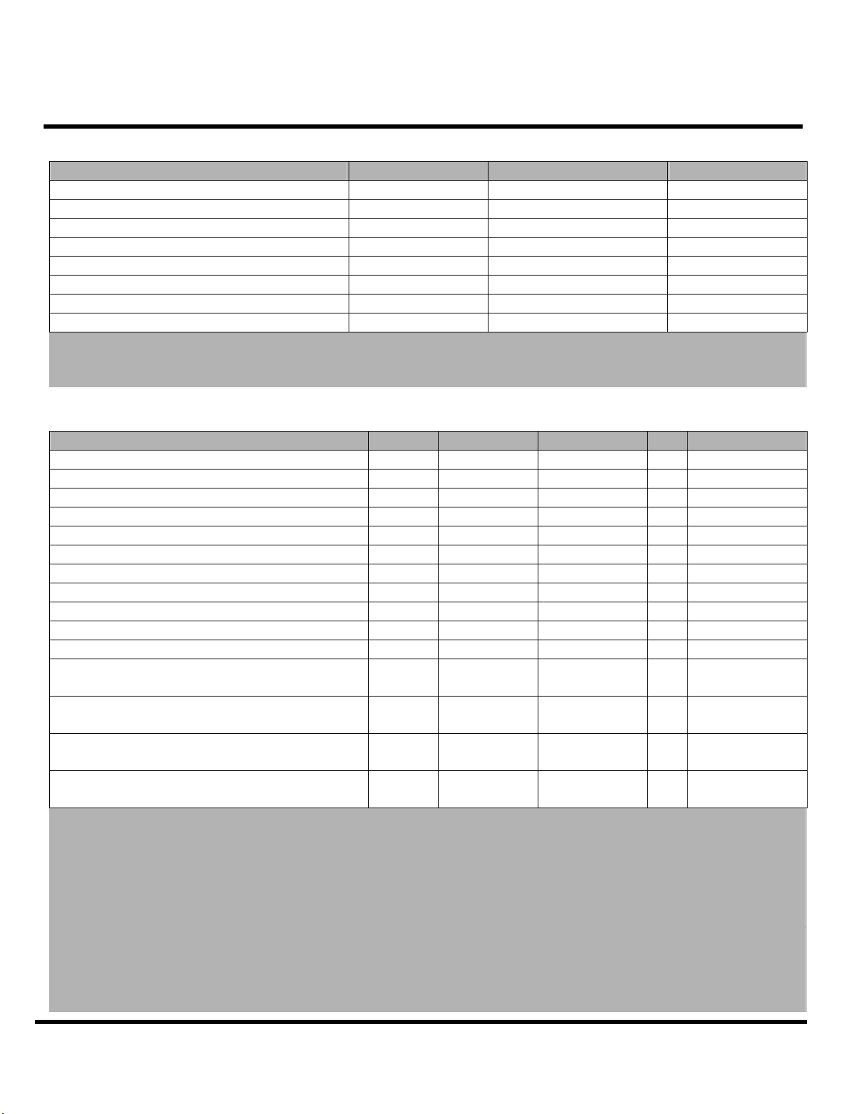
ABSOLUTE MAXIMUM RATINGS
Voltage on any pin relative to Vss VIN, VOUT -0.5 ~ 3.6 V
Voltage on VDD supply to Vss VDD, VDDQ -1.0 ~ 3.6 V
Storage temperature TSTG -55~+150 °C
Power dissipation PD 48 W
Short circuit current IOS 50 mA
Mean time between failure MTBF 50 year
Temperature Humidity Burning THB 85°C/85%, Static Stress °C-%
Temperature Cycling Test TC 0°C ~ 125°C Cycling °C
Note: Permanent device damage may occur if ABSOLUTE MAXIMUM RATINGS are exceeded.
Functional operation should be restricted to recommended operating condition.
Exposure to higher than recommended voltage for extended periods of time could affect device reliability.
DC OPERATING CONDITIONS
Recommended operating conditions (Voltage referenced to Vss = 0V, TA = 0 to 70°C)
Supply voltage VDD 2.3 2.7 V
I/O Supply voltage VDDQ 2.3 2.7 V
I/O Reference voltage VREF VDDQ/2-50mV VDDQ/2+50mV V 1
I/O Termination voltage VTT VREF-0.04 VREF+0.04 V 2
Input logic high voltage VIH(DC) VREF+0.15 VDDQ+0.3 V 4
Input logic low voltage VIL(DC) -0.3 VREF-0.15 V 4
Input Voltage Level, CK and /CK inputs VIN(DC) -0.3 VDDQ+0.3 V
Input Differential Voltage, CK and /CK inputs VID(DC) 0.3 VDDQ+0.6 V 3
Input crossing point voltage, CK and /CK inputs VIX(DC) 1.15 1.35 V 5
Input leakage current II -2 2 uA
Output leakage current IOZ -5 5 uA
Output High Current (Normal strength driver)
VOUT= VTT + 0.84V
Output Low Current (Normal strength driver)
VOUT= VTT – 0.84V
Output High Current (Half strength driver)
VOUT= VTT + 0.45V
Output High Current (Half strength driver)
VOUT= VTT - 0.45V
Note:
T
1
S
1
S
1. Includes ± 25mV margin for DC offset on VREF, and a combined total of ± 50mV margin for all AC noise and
2. VTT is not applied directly to the device. VTT is a system supply for signal termination resistors, is expected to
3. VID is the magnitude of the difference between the input level on CK and the input level on /CK.
4. These parameters should be tested at the pin on actual components and may be checked at either the pin or
5. The value of VIX is expected to equal 0.5*VDDQ of the transmitting device and must track variations in the dc
M
8
2
M
8
2
DC offset on VREF, bandwidth limited to 20MHz. The DRAM must accommodate DRAM current spikes on
VREF and internal DRAM noise coupled. TO VREF, both of which may result in VREF noise. VREF should be
de-coupled with an inductance of <=3nH.
be set equal to VREF, and must track variations in the DC level of VREF
the pad in simulation. The AC and DC input specifications are relative to a VREF envelop that has been
bandwidth limited to 200MHZ.
level of the same.
D
L
D
L
Parameter Symbol Value Unit
Parameter Symbol Min Max Unit Note
6
6
4
4
V
V
6
6
E
E
I
OH -16.8 mA
I
OL 16.8 mA
I
OH -9 mA
I
OL 9 mA
1GB With 64Mx4 CL2.5
Transcend Information Inc.
5
Page 6
184PIN DDR266 Unbuffered DIMM
E
6
V
4
6
D
L
M
8
2
1
S
T
T
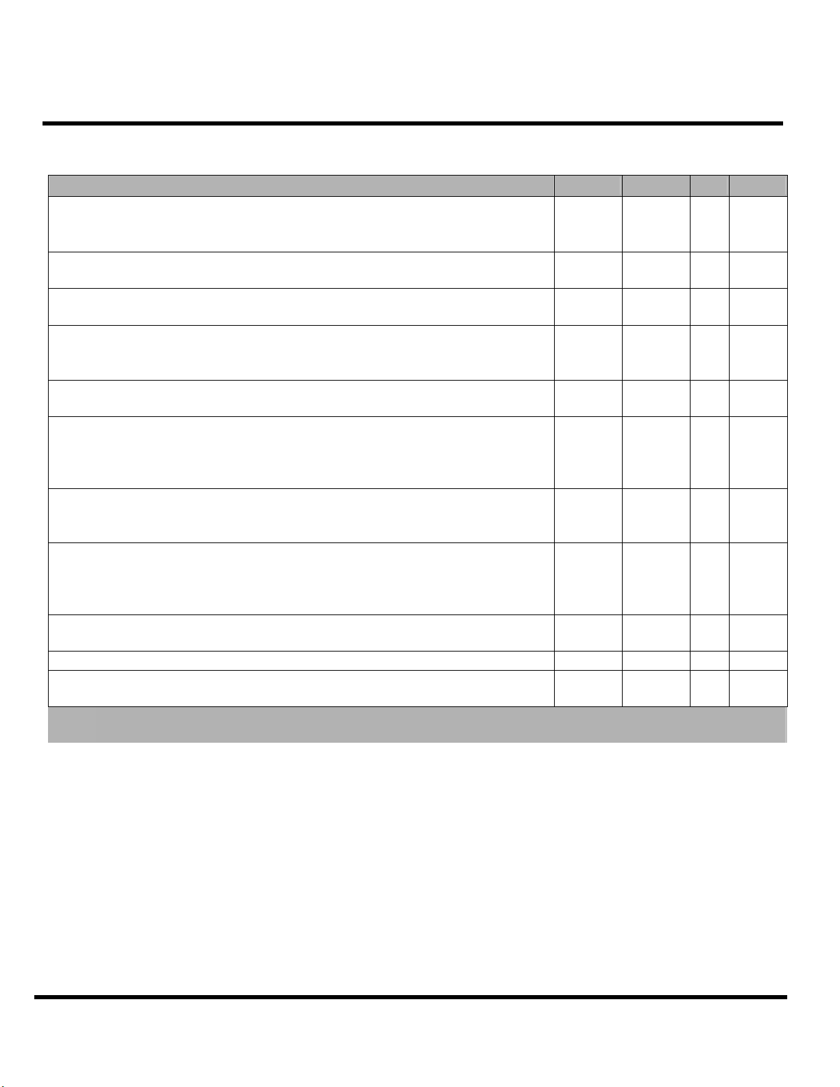
DC CHARACTERISTICS
(Recommended operating condition unless otherwise noted, VDD=2.7V TA = 10°C)
Operating current - One bank Active-Precharge; tRC=tRCmin;
DQ, DM and DQS inputs changing twice per clock cycle;
Address and control inputs changing once per clock cycle
Operating current - One bank operation; One bank open, Burst=4; Reads
- Refer to the following page for detailed test condition.
Precharge power-down standby current; All banks idle; power –down mode;
CKE = <VIL (max); VIN = VREF for DQ,DQS and DM
Precharge Floating standby current; CS# > =VIH(min);All banks idle;
CKE > = VIH(min); Address and other control inputs changing once per clock
cycle; VIN = VREF for DQ,DQS and DM
Active power - down standby current; one bank active; power-down mode;
CKE<= VIL (max); VIN = VREF for DQ, DQS and DM
Active standby current; CS# >= VIH (min); CKE>=VIH(min);
one bank active; active - precharge; tRC=tRASmax;
DQ, DQS and DM inputs changing twice per clock cycle;
address and other control inputs changing once per clock cycle
Operating current - burst read; Burst length = 2; reads; continuous burst;
One bank active; address and control inputs changing once per clock cycle;
50% of data changing at every burst; lout = 0 mA
Operating current - burst write; Burst length = 2; writes; continuous burst;
One bank active address and control inputs changing once per clock cycle;
DQ, DM and DQS inputs changing twice per clock cycle,
50% of input data changing at every burst
Auto refresh current; tRC = tRFC(min),
10*tCK for DDR266at 133Mhz; distributed refresh
Self refresh current; CKE <= 0.2V; External clock should be on;
Operating current - Four bank operation; Four bank interleaving with BL=4
-Refer to the following page for detailed test condition
Note: Module IDD was calculated on the basis of component IDD and can be differently measured according to DQ
T
1
S
1
S
loading cap.
2
2
8
8
M
M
L
L
D
D
6
6
V
4
V
4
Parameter Symbol Max. Unit Note
6
6
E
E
1GB With 64Mx4 CL2.5
IDD0 2570 mA
IDD1 3075 mA
IDD2P 1242 mA
IDD2F 1586 mA
IDD3P 1676 mA
IDD3N 1900 mA
IDD4R 3420 mA
IDD4W 2880 mA
IDD5 3620 mA
IDD6 398 mA
IDD7 5665 mA
Transcend Information Inc.
6
Page 7
184PIN DDR266 Unbuffered DIMM
E
6
V
4
6
D
L
M
8
2
1
S
T
T
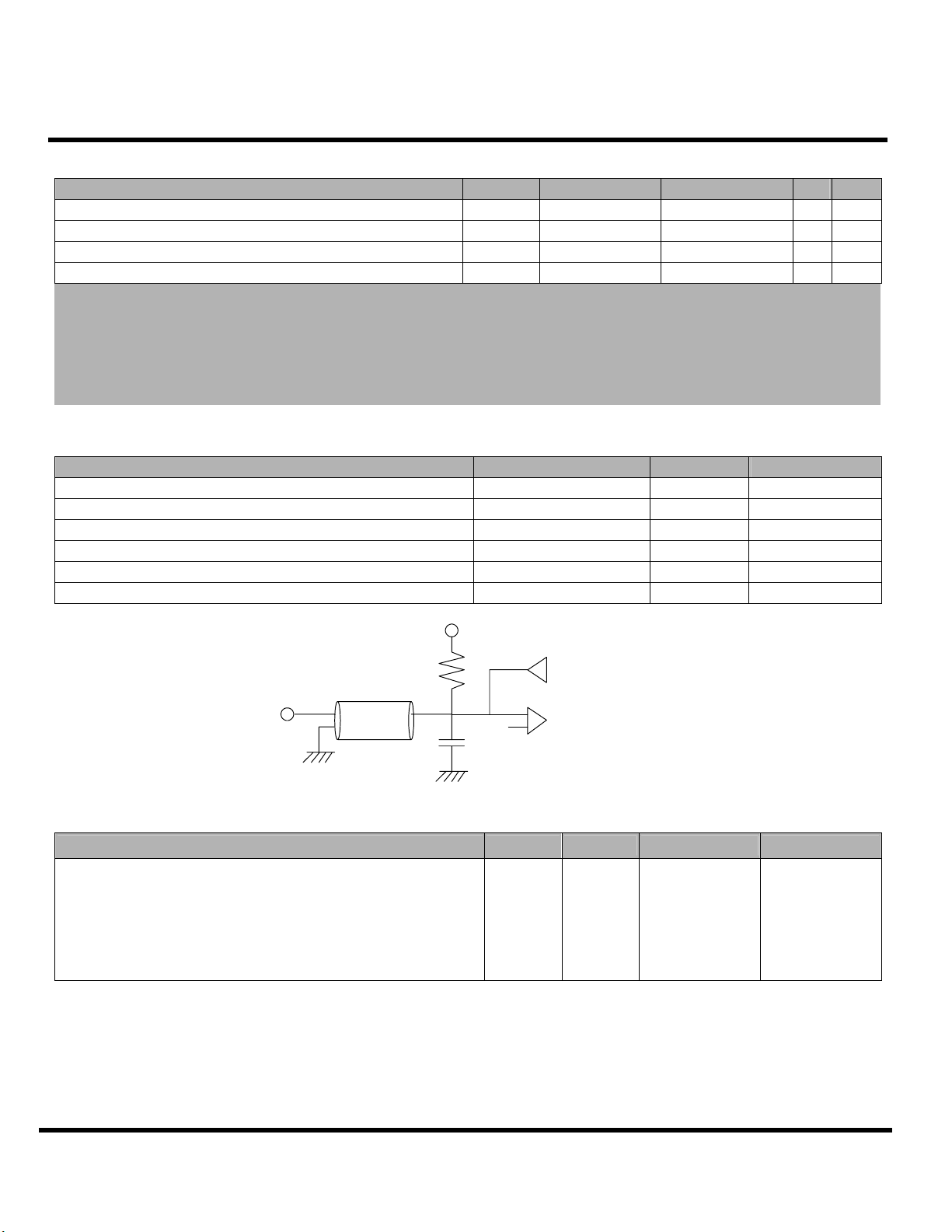
AC OPERATING CONDITIONS
Input High (Logic 1) Voltage, DQ, DQS and DM signal VIH(AC) VREF + 0.31 V 3
Input Low (Logic 0) Voltage, DQ, DQS and DM signal VIL(AC) VREF - 0.31 V 3
Input Differential Voltage, CK and /CK inputs VID(AC) 0.7 VDDQ + 0.6 V 1
Input Crossing Point Voltage, CK and /CK inputs VIX(AC) 0.5*VDDQ - 0.2 0.5*VDDQ + 0.2 V 2
Note: 1. VID is the magnitude of the difference between the input level on CK and the input on /CK.
2. The value of VIX is expected to equal 0.5*V DDQ of the transmitting device and must track variations in the
3. These parameters should be tested at the pin on actual components and may be checked at either the pin or
AC OPERATING TEST CONDITIONS (VDD=2.5, VDDQ=2.5, TA=0 to 70°C)
Input reference voltage for Clock 0.5*VDDQ V
Input signal maximum peak swing 1.5 V
Input Levels(VIH/VIL) VREF+0.31/VREF-0.31 V
Input timing measurement reference level VREF V
Output timing measurement reference level VTT V
Output load condition See Load Circuit
T
S
S
1
1
M
8
2
M
8
2
DC level of the same.
the pad in simulation. The AC and DC input specifications are relative to a VREF envelope that has been
bandwidth limited 20MHz.
D
L
D
L
Parameter Symbol Min Max Unit Note
Parameter Value Unit Note
6
6
4
4
V
V
6
6
E
E
VTT=0.5*VDDQ
1GB With 64Mx4 CL2.5
RT=50ohm
Output
Input/Output CAPACITANCE (VDD = 2.5V, VDDQ = 2.5V,TA = 25°C, f = 1MHz)
Parameter Symbol Min Max Unit
Input capacitance (A0~A12, BA0~BA1, /RAS, /CAS, /WE)
Input capacitance (CKE0, CKE1)
Input capacitance (/CS0, /CS1)
Input capacitance (CK0~CK2, /CK0~/CK2)
Input capacitance (DM0~DM7)
Data and DQS input/output capacitance (DQ0~DQ63)
ZO=50ohm
LOAD
=30pF
C
Output Load circuit
VREF
=0.5*VDDQ
C
IN1
CIN2
C
IN3
CIN4
CIN5
C
OUT1
64
42
42
27
12
12
96
50
50
34
14
14
pF
pF
pF
pF
pF
pF
Transcend Information Inc.
7
Page 8
184PIN DDR266 Unbuffered DIMM
E
6
V
4
6
D
L
M
8
2
1
S
T
T
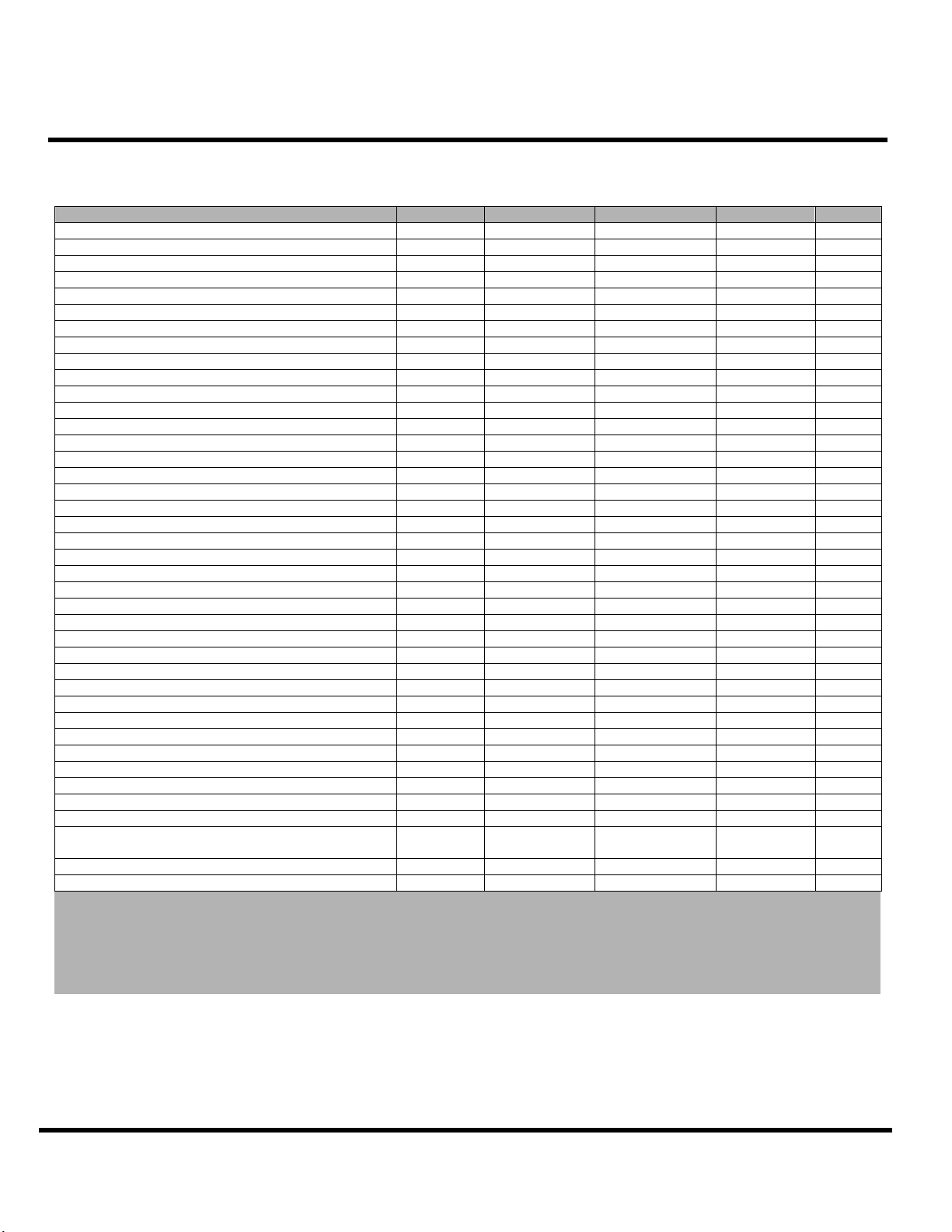
AC Timing Parameters & Specifications
(These AC characteristics were tested on the Component)
Row cycle time tRC 65 ns
Refresh row cycle time tRFC 75 ns
Row active time tRAS 45 120K ns
/RAS to /CAS delay tRCD 20 ns
Row active to Row active delay tRP 20 ns
Row active to Row active delay tRRD 15 ns
Write recovery time tWR 15 ns
Last data in to Read command tCDLR 1 tCK
Col. Address to Col. Address delay tCCD 1 tCK
Clock cycle time tCK 7.5 12 ns
Clock high level width tCH 0.45 0.55 tCK
Clock low level width tCL 0.45 0.55 tCK
DQS-out access time from CK /CK tDQSCK -0.75 0.75 ns
Output data access time from CK /CK tAC -0.75 0.75 ns
Data strobe edge to output data edge tDQSQ 0.5 ns
Read Preamble tRPRE 0.9 1.1 tCK
Read Postamble tRPST 0.4 0.6 tCK
CK to valid DQS-in tDQSS 0.75 1.25 tCK
DQS-in setup time tWPRES 0 ns 2
DQS-in hold time tWPREH 0.25 tCK
DQS falling edge to CK rising-setup time tDSS 0.2 tCK
DQS falling edge from CK rising-hold time tDSH 0.2 tCK
DQS-in high level width tDQSH 0.35 tCK
DQS-in low level width tDQSL 0.35 tCK
DQS-in cycle time tDSC 0.9 1.1 tCK
Address and Control input setup time tIS 0.9 ns
Address and Control input hold time tIH 0.9 ns
Data-out high-impedance time from CK, /CK tHZ -0.75 0.75 ns
Data-out low-impedance time from CK, /CK tLZ -0.75 0.75 ns
Mode register set cycle time tMRD 15 ns
DQ & DM setup time to DQS tDS 0.5 ns
DQ & DM hold time to DQS tDH 0.5 ns
DQ & DM input pulse width tDIPW 1.75 ns
Power down exit time tPDEX 7.5 ns
Exit self refresh to non-Read command tXSNR 75 ns
Exit self refresh to read command tXSRD 200 tCK
Refresh interval time tREF 7.8 us 1
Clock half period
Data hold skew factor tQHS 0.75 ns
DQS write postamble time tWPST 0.4 0.6 tCK 3
Note: 1. Maximum burst refresh of 8
2. The specific requirement is that DQS be valid (High or Low) on or before this CK edge. The case shown
3. The Maximum limit for this parameter is not a device limit. The device will operate with a great value for this
T
S
S
1
1
M
8
2
M
8
2
(DQS going from High_Z to logic Low) applies when no writes were previously in progress on the bus. If a
previous write was in progress, DQS could be High at this time, depending on tDQSS.
parameter, but system performance (bus turnaround) will degrade accordingly.
D
L
D
L
Parameter Symbol Min Max Unit Note
6
6
4
4
V
V
6
6
E
E
tHP tCLmin or
1GB With 64Mx4 CL2.5
ns
tCHmin
Transcend Information Inc.
8
Page 9
184PIN DDR266 Unbuffered DIMM
E
6
V
4
6
D
L
M
8
2
1
S
T
T
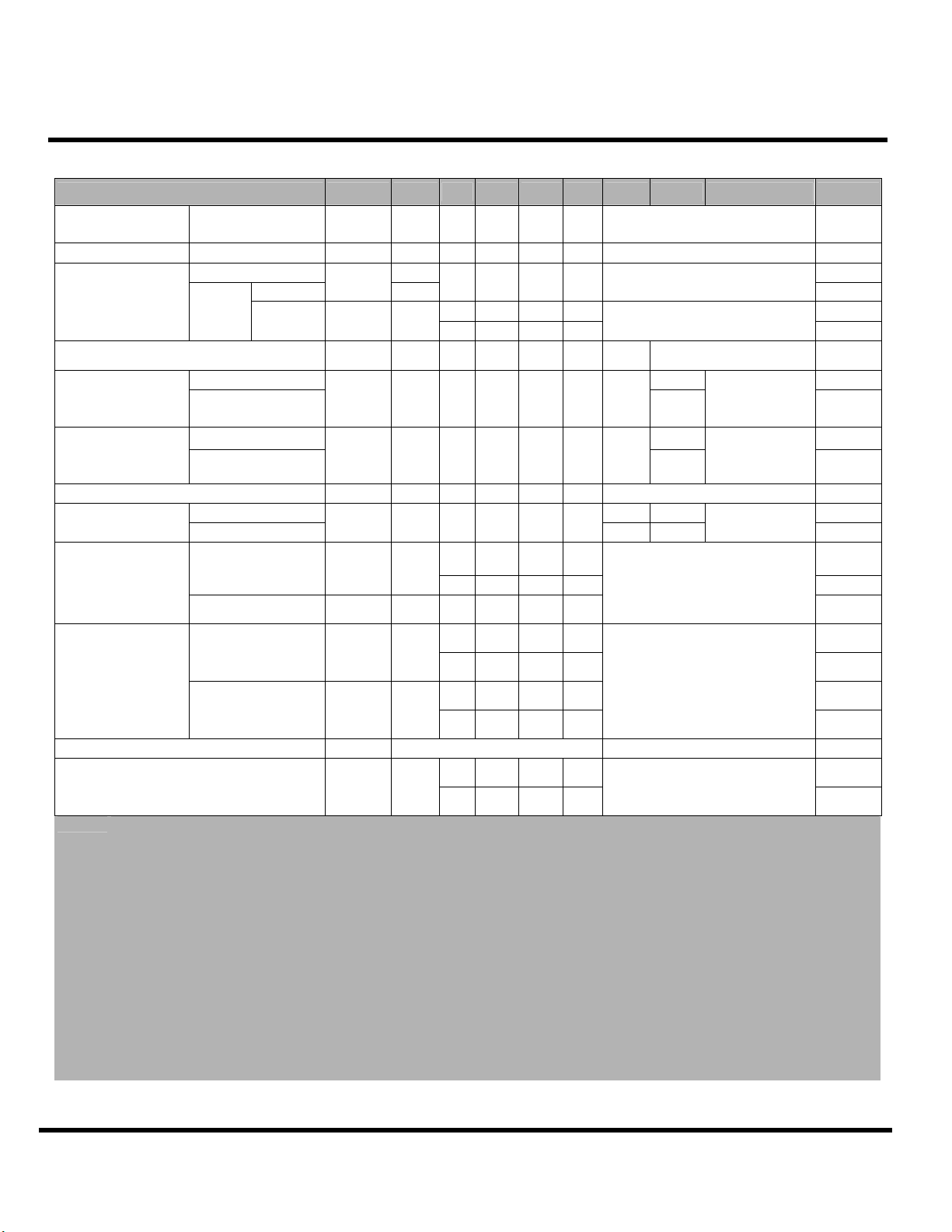
SIMPLIFIED TRUTH TABLE (V=Valid, X=Don’t Care, H=Logic High, L=Logic Low)
Register
Register Mode Register Set H X L L L L OP CODE 1,2
Refresh
Bank Active & Row Addr. H X L L H H V Row Address
Read &
Column Address
Write &
Column Address
Burst Stop H X L H H L X 7
Precharge
T
S
S
1
1
M
8
2
M
8
2
COMMAND CKEn-1 CKEn /CS /RAS /CAS /WE BA0,1 A10/AP A0~A9,A11, A12 Note
D
L
D
L
Extended
Mode Register Set
Auto Refresh H 3
Self
Refresh
Auto Precharge Disable L 4
Auto Precharge Enable
Auto Precharge Disable L 4
Auto Precharge Enable
Bank Selection V L
All Banks
V
4
6
V
4
6
Entry
Exit L H
E
6
E
6
H X L L L L OP CODE 1,2
H
H X L H L H V
H X L H L L V
H X L L H L
L L L H X
L
L H H H 3
H X X X
X H
1GB With 64Mx4 CL2.5
X
Column
H
H
Address
(A0~A9, A11)
Column
Address
(A0~A9, A11)
X
3
3
4
4, 6
5
Active Power Down
Precharge Power
Down Mode
DM H X X 8
No Operation Command
Note: OP Code: Operand Code. A0 ~ A12 & BA0 ~ BA1: Program keys. (@EMRS/MRS)
EMRS/ MRS can be issued only at all banks precharge state.
A new command can be issued 2 clock cycles after EMRS or MRS.
Auto refresh functions are same as the CBR refresh of DRAM.
The automatically precharge without row precharge command is meant by "Auto".
Auto/self refresh can be issued only at all banks precharge state.
BA0 ~ BA1: Bank select addresses. If both BA0 and BA1 are "Low" at read, write, row active and precharge, bank A is selected.
If both BA0 is "High" and BA1 is "Low" at read, write, row active and precharge, bank B is selected.
If both BA0 is "Low" and BA1 is "High" at read, write, row active and precharge, bank C is selected.
If both BA0 and BA1 are "High" at read, write, row active and precharge, bank D is selected.
If A10/AP is "High" at row precharge, BA0 and BA1 are ignored and all banks are selected.
During burst write with auto precharge, new read/write command cannot be issued.
Another bank read/write command can be issued after the end of burst.
New row active of the associated bank can be issued at tRP after the end of burst.
Burst stop command is valid at every burst length.
DM sampled at the rising and falling edges of the DQS and Data-in is masked at the both edges (Write DM latency is 0).
This combination is not defined for any function, which means "No Operation (NOP)" in DDR SDRAM.
Entry H L
Exit L H X X X X
Entry
Exit
H L
L H
H X
H X X X
L V V V
H X X X
L H H H
H X X X
L V V V
H X X X 9
L H H H
X
X
X
9
Transcend Information Inc.
9
Page 10
184PIN DDR266 Unbuffered DIMM
E
6
V
4
6
D
L
M
8
2
1
S
T
T
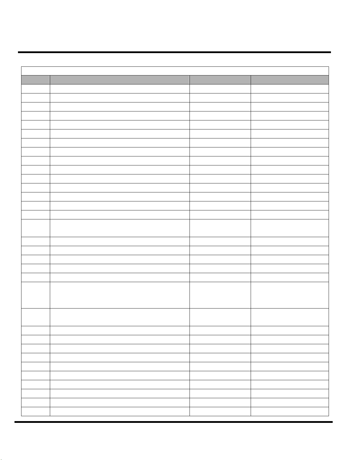
Serial Presence Detect Specification
1
S
1
S
T
Byte No. Function Described Standard Specification Vendor Part
0 # of Bytes Written into Serial Memory 128bytes 80
1 Total # of Bytes of S.P.D Memory 256bytes 08
2 Fundamental Memory Type DDR SDRAM 07
3 # of Row Addresses on this Assembly 13 0D
4 # of Column Addresses on this Assembly 11 0B
5 # of Module Rows on this Assembly 2 bank 02
6 Data Width of this Assembly 64bits 40
7 Data Width of this Assembly 0 00
8 VDDQ and Interface Standard of this Assembly SSTL 2.5V 04
9 DDR SDRAM Cycle Time at CAS Latency=2.5 7.5ns 75
10 DDR SDRAM Access Time from Clock at CL=2.5 ±0.75ns 75
11 DIMM configuration type (non-parity, Parity, ECC) Non-parity 00
12 Refresh Rate Type 7.8us/Self Refresh 82
13 Primary DDR SDRAM Width X8 08
14 Error Checking DDR SDRAM Width N/A 00
15 Min Clock Delay for Back to
16 Burst Lengths Supported 2,4,8 0E
17 # of banks on each DDR SDRAM device 4 bank 04
18 CAS Latency supported 2, 2.5 0C
19 CS Latency 0 CLK 01
20 WE Latency 1 CLK 02
21 DDR SDRAM Module Attributes
22 DDR SDRAM Device Attributes: General
23 DDR SDRAM Cycle Time CL=2.0 10ns A0
24 DDR SDRAM Access from Clock CL=2.0 ±0.75ns 75
25 DDR SDRAM Cycle Time CL=1.5 - 00
26 DDR SDRAM Access from Clock CL=1.5 - 00
27 Minimum Row Precharge Time (tRP) 20ns 50
28 Minimum Row Active to Row Activate delay (tRRD) 15ns 3C
29 Minimum RAS to CAS Delay (tRCD) 20ns 50
30 Minimum active to Precharge time (tRAS) 45ns 2D
31 Module ROW density 512MB 80
32 Command/Address Input Setup Time 0.9ns 90
M
8
2
M
8
2
Back Random Column Address
L
L
D
D
6
6
4
4
V
V
6
6
E
E
Serial Presence Detect
1GB With 64Mx4 CL2.5
TCCD=1CLK 01
Registered address &
control inputs and
on-card DLL
+/-0.2V voltage
tolerance
20
00
Transcend Information Inc.
10
Page 11
184PIN DDR266 Unbuffered DIMM
E
6
V
4
6
D
L
M
8
2
1
S
T
T
1
S
1
S
T
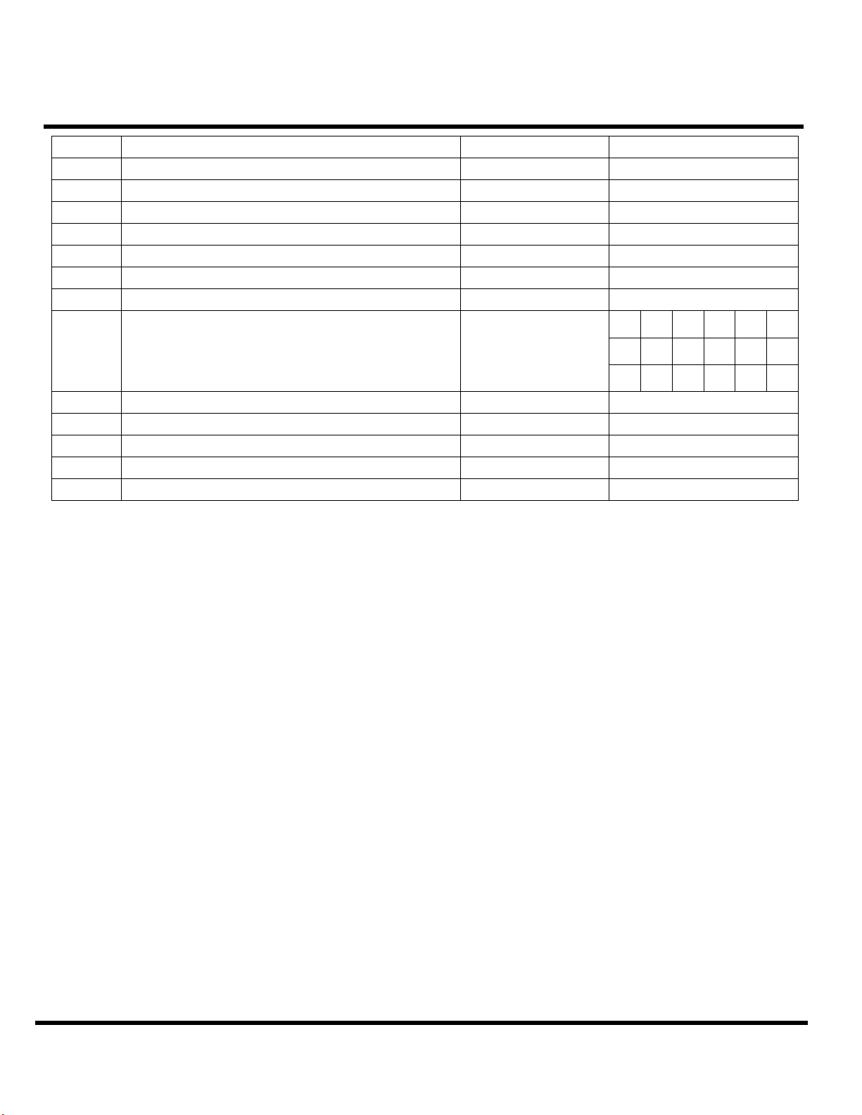
33 Command/Address Input Hold Time 0.9ns 90
34 Data Signal Input Setup Time 0.5ns 50
35 Data Signal Input Hold Time 0.5ns 50
36-61 Superset Information - 00
62 SPD Data Revision Code - 00
63 Checksum for Bytes 0-62 - 01
64-71 Manufacturers JEDEC ID Transcend 7F, 4F
72 Manufacturing Location T 54
2
2
8
8
M
M
L
L
D
D
6
6
4
4
V
V
6
6
E
E
1GB With 64Mx4 CL2.5
54 53 31 32 38 4D
73-90 Manufacturers Part Number TS128MLD64V6E
91-92 Revision Code - 00
93-94 Manufacturing Date By Manufacturer Variable
95-98 Assembly Serial Number By Manufacturer Variable
99-127 Manufacturer Specific Data - 00
128~255 Unused Storage Locations Undefined 00
4C 44 36 34 56 36
45 20 20 20 20 20
Transcend Information Inc.
11
 Loading...