

Page 1

QUICK START GUIDE FOR DEMONSTRATION CIRCUIT 1060
DESCRIPTION
DUAL MONOLITHIC STEP-DOWN SWITCHING REGULATOR
LT3508
Demonstration circuit 1060 features two LT3508
step-down DC/DC switching converters. One circuit
uses the LT3508EFE and the other circuit has the
LT3508EUF. The LT3508 dual output step-down
switching regulator has two internal power
switches, a wide input voltage range, adjustable
switching frequency synchronizable over the frequency range, programmable soft-start, tracking,
power-good, and channel sequencing. The antiphase switching reduces the input capacitor. The
wide V
configurations with up to 36V input. The high power
internal switches have current limit that allows for
up to 1.4A output on each output.
The demonstration circuit has two circuits. The top
is optimized for high efficiency, wide input range
and maximum output current; the bottom is optimized for the size. The top circuit is rated for 3.3V
at 1.4A and 5V at 1.4A output from a 6V–36V input
using the FE package. The frequency is set to
700kHz to allow for the high VIN to VOUT ratio and
provides high efficiency throughout the range. The
bottom circuit generates 1.8V at 1A and 3.3V at 1A
from a 5V to 16V DC input using the QFN package
and shows off the compact size with 1.6MHz
range of the LT3508 allows step-down
IN
switching frequency. The two channels are sequenced so that the 1.8V channel starts before the
3.3V channel. The two circuits are completely isolated from each other and can be run simultaneously or independently. The shutdown terminals are
available on each circuit as are the power good and
track terminals in case sequencing or tracking is
preferred.
This board is designed for applications that require
two step-down converters up to 1.4A load with low
cost, small board space, low parts count, and simple circuit design. The high current, on-board, dual
monolithic switches eliminate the need for external
switches. The current-mode control simplifies the
compensation network and gives excellent transient
response.
Please read the LT3508 datasheet in addition to this
quickstart guide for details regarding LT3508 operation and applications.
Design files for this circuit board are available.
Call the LTC factory.
LT is a trademark of Linear Technology Corporation
1
Page 2
QUICK START GUIDE FOR DEMONSTRATION CIRCUIT 1060
TYPICAL PERFORMANCE (TA = 25°C)
DUAL MONOLITHIC STEP-DOWN SWITCHING REGULATOR
100%
3.3V , 5V
95%
ou tp u t s
90%
85%
12V IN
80%
75%
E FF IC IEN CY (% )
70%
65%
60%
18V IN
0 0.5 1 1 .5
C H1, C H2 LO AD C UR RE NT (mA )
6V IN
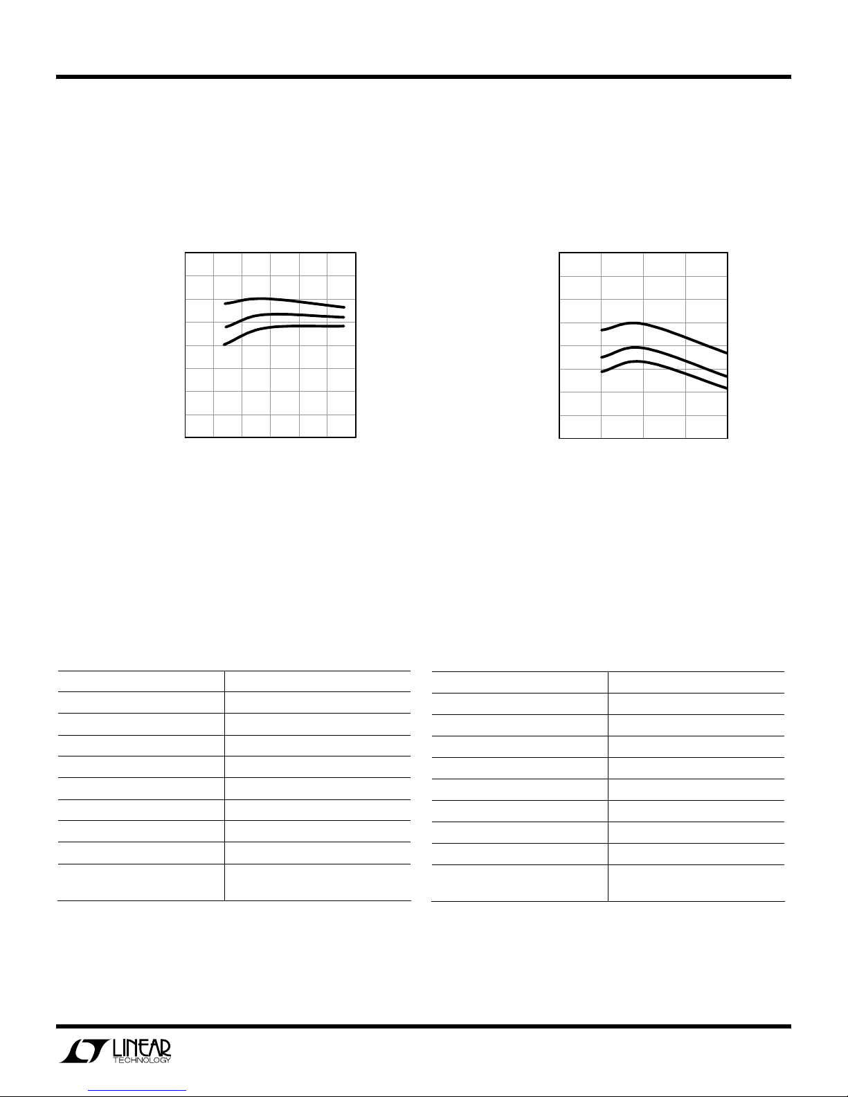
Figure 1. Typical Efficiency of DC1060A LT3508EFE Dual Step-
Down VOUT1=3.3V, VOUT2=5V
Table 1. FE package Dual Step-Down Converter (VOUT1=3.3V
and VOUT2=5V)
Parameter Value
VIN 6V to 36V
V
OUT1
3.3V
V
2 5V
OUT
V
1 Load Current 1.4A(max)
OUT
V
2 Load Current 1.4A(max)
OUT
Switching frequency 700kHz
V
1 Ripple pk-pk 25mV at 1.4A and 18VIN
OUT
V
2 Ripple pk-pk 18mV at 1.4A and 18VIN
OUT
Efficiency
86% at 1.4A load current (VOUT1
and VOUT2) and 12VIN
100%
1.8V , 3.3V
95%
ou tp u t s
90%
85%
80%
12V IN
75%
E FF IC IE NC Y (%)
70%
65%
60%
0 0.2 5 0.5 0.75 1
C H1, C H2 LO A D C UR RE NT (mA )
5V IN
16V IN
Figure 2. Typical Efficiency of DC1060A LT3508EUF Dual Step-
Down VOUT1=1.8V, VOUT2=3.3V
Table 2. QFN Package Dual Step-Down Converter (VOUT1=1.8V
and VOUT2=3.3V)
Parameter Value
VIN 5V to 16V
VOUT1 1.8V
VOUT2 3.3V
VOUT1 Load Current 1A(max)
VOUT2 Load Current 1A(max)
Switching frequency 1.6MHz
V
1 Ripple pk-pk 3mV at 1A and 12VIN
OUT
V
2 Ripple pk-pk 5mV at 1A and 12VIN
OUT
Efficiency
85% at 500mA load current
(VOUT1 and VOUT2) and 5VIN
2
Page 3
QUICK START GUIDE FOR DEMONSTRATION CIRCUIT 1060
DUAL MONOLITHIC STEP-DOWN SWITCHING REGULATOR
QUICK START PROCEDURE
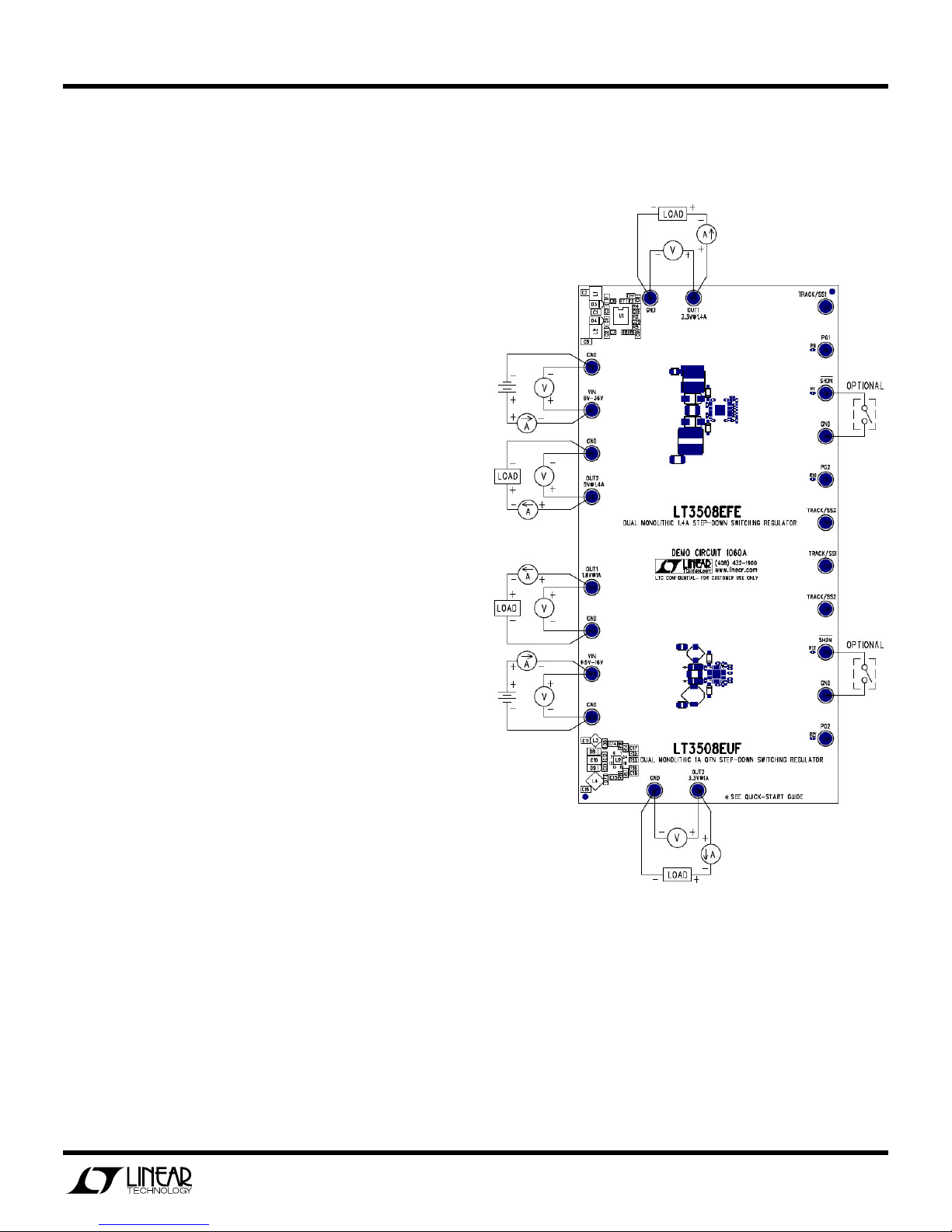
DC1060A is easy to set up to evaluate the performance of the LT3508. Refer to Figure 3 for proper
measurement equipment setup and follow the procedure below:
LT3508EFE top circuit:
1.
Connect a 6V–36V DC input power supply to the
VIN and GND terminals on the board with power
OFF.
2.
Attach the desired load to each channel – up to
1.4A.
3.
After all connections are made, turn ON input
power and verify that the output voltages are 3.3V
and 5V.
4.
The Track/SS, power good (PG), and shutdown
functions are optional and their terminals can be
left floating (disconnected). Connecting the shutdown terminal to the GND terminal shuts down the
circuit and drops the output voltages to zero. Shutdown has a pull-up resistor on circuit that may not
be necessary with the proper high and low signal
applied.
LT3508EUF bottom circuit
1.
Use the same testing method for the bottom circuit as used in the top circuit, but with a different
input voltage (5V to 16V), load currents (1A per
channel maximum), and output voltages (1.8V
and 3.3V).
2.
Upon startup, sequencing of VOUT1 and VOUT2
can be observed with an oscilloscope.
Figure 3. Proper Measurement Equipment Setup
SYNC FUNCTION
The Rt/Sync pin can be used for synchronization of the LT3508 internal oscillator to an external source. To use
the sync function, remove R2 (in the top FE circuit) or R13 (in the bottom UF circuit), and attach the external
sync signal to the Rt/Sync pin directly or to the now-unstuffed resistor pad tied to the Rt/Sync pin.
3
Page 4
QUICK START GUIDE FOR DEMONSTRATION CIRCUIT 1060
DUAL MONOLITHIC STEP-DOWN SWITCHING REGULATOR
4
Page 5

Mouser Electronics
Authorized Distributor
Click to View Pricing, Inventory, Delivery & Lifecycle Information:
Analog Devices Inc.:
DC1060A
 Loading...