

Datasheet 100398QIX, 100398QI, 100398QCX, 100398QC, 100398PC Datasheet (Fairchild Semiconductor)
Page 1
© 2000 Fairchild Semiconductor Corporation DS010970 www.fairchildsemi.com
February 1992
Revised August 2000
100398 Quad Differential ECL/TTL Translating Transceiver with Latch
100398
Quad Differential ECL/TTL Translating Transceiver
with Latch
General Description
The 100398 is a quad latched transceiver designed to convert TTL logic levels to differential F100K ECL logic levels
and vice versa. This device was desig ned wit h the capa bi lity of driving a differential 25
Ω ECL load with cutoff capabil-
ity, and will sink a 64 mA TTL load. The 100398 is ideal for
mixed technology applications utilizing either an ECL or
TTL backplane.
The direction of translat ion is set by the direction control
pin (DIR). The DIR pin on the 100398 accept s TTL logic
levels. A TTL LOW on DIR sets up the ECL pi ns as inputs
and TTL pins as ou tputs. A TTL HIG H on DIR sets up the
TTL pins as inputs and ECL pins as outputs.
A LOW on the outp ut en able inp ut pi n (OE) hol ds the ECL
output in a cut-off state and the TTL outputs at a high
impedance level. A HIGH on the latch enable input (LE)
latches the data at both inputs even though only one output
is enabled at the time. A LOW on LE makes the latch transparent.
The cut-off state is designe d to be more negative than a
normal ECL LOW l evel. This allows the output emi tter-followers to turn off when the termination supply is
−2.0V, pre-
senting a high impedance to the data bus. This high
impedance reduces termination power and prevents loss of
low state noise margin when several loads share the bus.
The 100398 is designe d with FAST
TTL output buffers,
featuring optimal DC drive an d capabl e of quickly cha rging
and discharging highly capacitive loads. All Inputs have
50 k
Ω pull-down resistors.
Features
■ Differential ECL input/output structure
■ 64 mA FAST TTL outputs
■ 25
Ω differential ECL outputs with cut-off
■ Bi-directional translation
■ 2000V ESD protection
■ Latched outputs
■ 3-STATE outputs
■ Voltage compensated operating range
= −4.2V to −5.7V
Ordering Code:
Devices also availab le in Tape and Reel. Specify by appending th e s uffix let t er “X” to the ordering code.
FAST is a registered trademark of Fairc hild Semiconductor.
Order Number Package Number Package Description
100398PC N24E 24-Lead Plastic Dual-In-Line Package (PDIP), JEDEC MS-010, 0.400 Wide
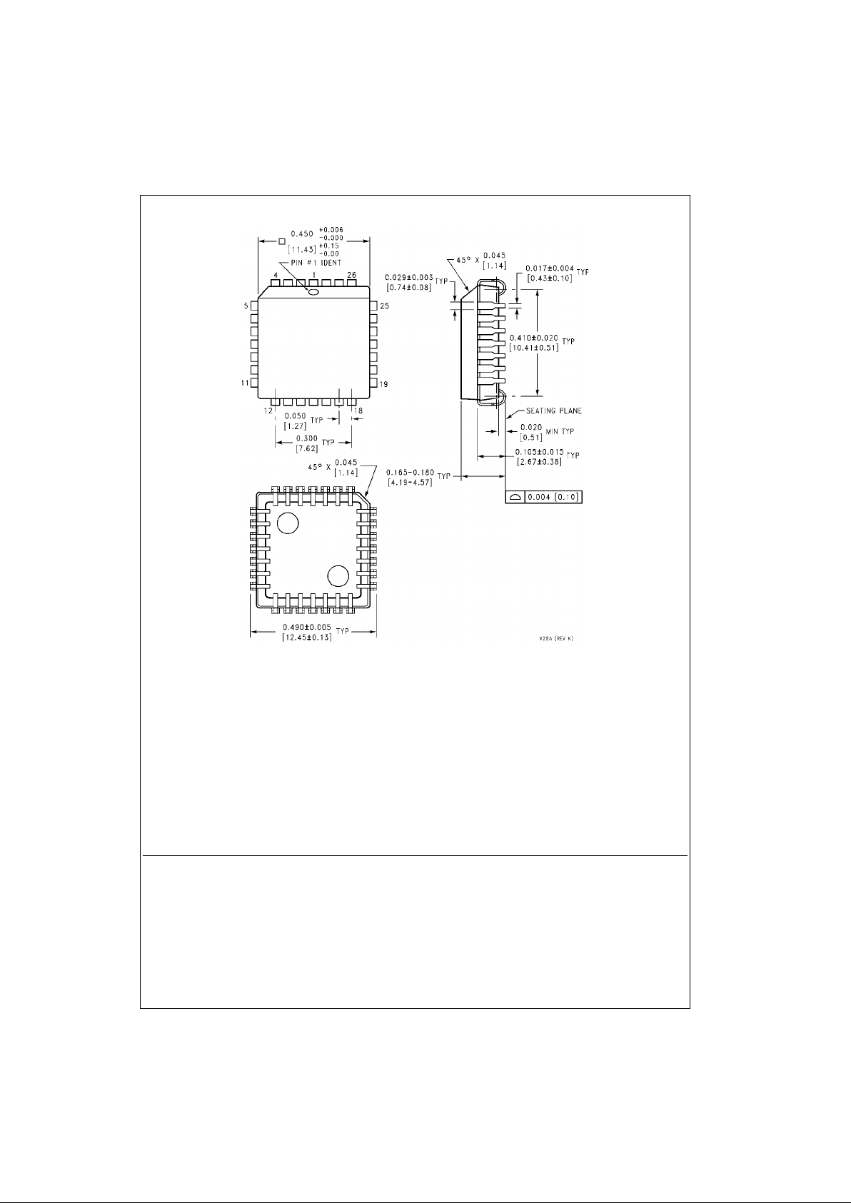
100398QC V28A 28-Lead Plastic Lead Chip Carrier (PLCC), JEDEC MO-047, 0.450 Square
100398QI V28A 28-Lead Plastic Lead Chip Carrier (PLCC), JEDEC MO-047, 0.450 Square
Industrial Temperature Range (
−40°C to +85°C)
Page 2
www.fairchildsemi.com 2
100398
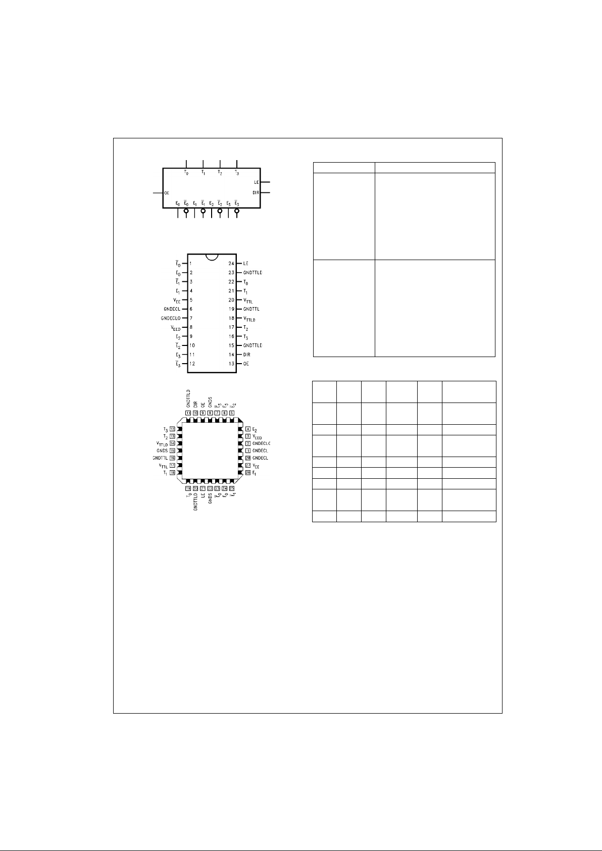
Logic Symbol
Connection Diagrams
24-Pin DIP
28-Pin PLCC
Pin Descriptions
Tr uth Table
H = HIGH Voltage Level
L = LOW Voltage Level
X = Don’t Care
Z = High Impedance
Note 1: ECL input to TTL out put mode.
Note 2: TTL input to ECL output mode.
Note 3: Retains data present before LE set HIGH.
Note 4: Latch is transparent.
Pin Names Description
E
0–E3
ECL Data I/O
E
0–E3
Complementary ECL
Data I/O
T
0–T3
TTL Data I/O
OE Output Enable Input Levels
LE Latch Enable Input Levels
DIR Direction Control
Input (TTL levels)
GNDECL ECL Ground
GNDECLO ECL Output Ground
GNDS ECL Ground-to-Substrate
V
EE
ECL Quiescent Power Supply
V
EED
ECL Dynamic Power Supply
GNDTTL TTL Quiescent Ground
GNDTTLD TTL Dynamic Ground
V
TTL
TTL Quiescent Power Supply
V
TTLD
TTL Dynamic Power Supply
LE DIR OE ECL TTL
Notes
Port Port
000LOWZ
(Cut-Off)
0 0 1 Input Output (Note 1)(Note 4)
010LOWZ
(Cut-Off)
0 1 1 Output Input (Note 2)(Note 4)
1 0 0 Input Z (Note 1)(Note 3)
1 0 1 Latched X (Note 1)(Note 3)
1 1 0 Low Input (Note 2)(Note 3)
(Cut-Off)
1 1 1 Latched X (Note 2)(Note 3)
Page 3
3 www.fairchildsemi.com
100398
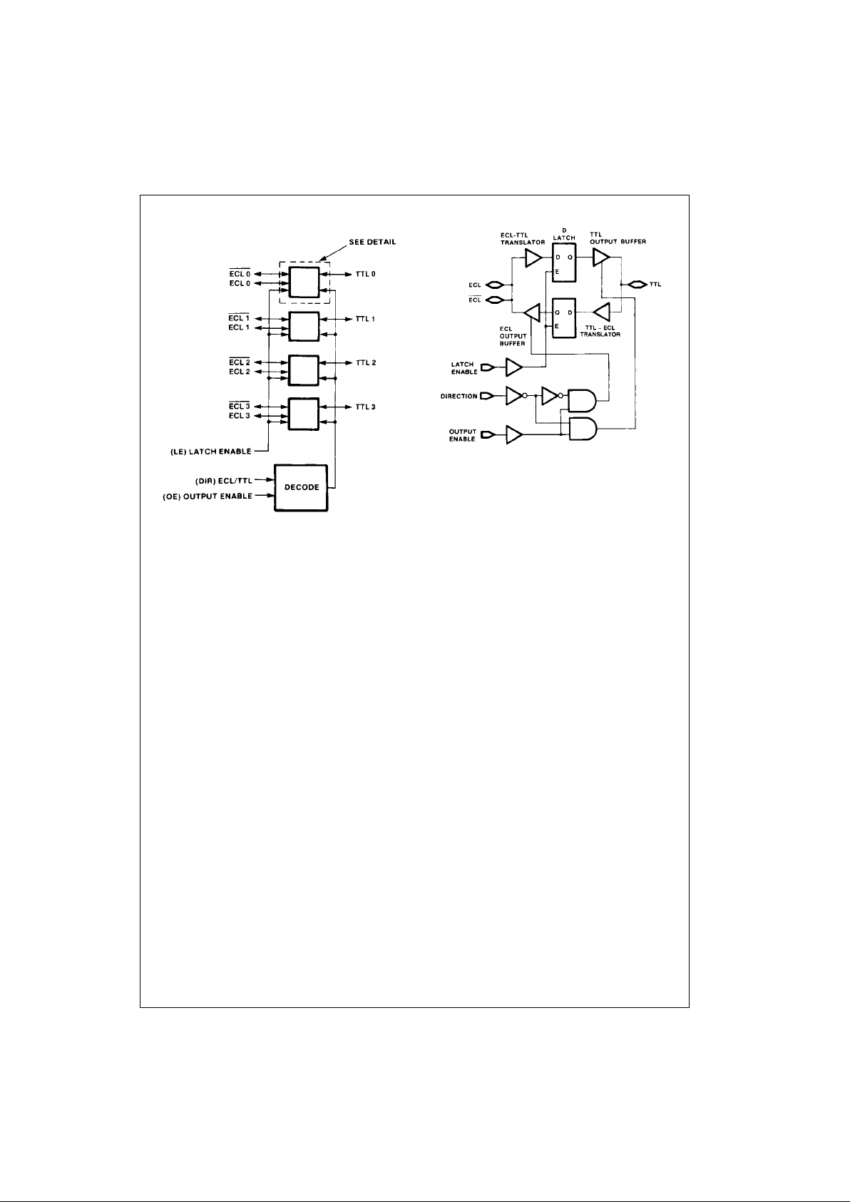
Functional Diagram
Note: LE, and OE use TTL logic levels
Detail
Page 4
www.fairchildsemi.com 4
100398
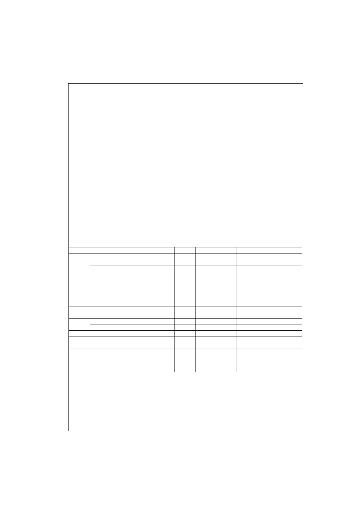
Absolute Maximum Ratings(Note 5) Recommended Operating
Conditions
Note 5: The “Absolute Maximum Ratings” are those values beyon d which
the safety of the dev ice cannot be guaranteed. T he device sh ould not be
operated at these limit s. The parametric values defin ed in the Electrical
Characteristics tables are not guaranteed at the absolute maximum rating.
The “Recomme nded O peratin g Cond itions ” table will defin e the condition s
for actual device operation.
Note 6: The specified limits represent t he “worst case” value for the param-
eter. Since these value s normally occur at th e temperature extrem es, additional noise immunity and guardbanding can be achieved by decreasing the
allowable system operating ranges. Conditions for testing shown in the
tables are chosen to guarantee operation under “worst case” conditions.
Note 7: ESD testing conf orm s t o M I L-STD-883, Method 3015.
Commercial Version
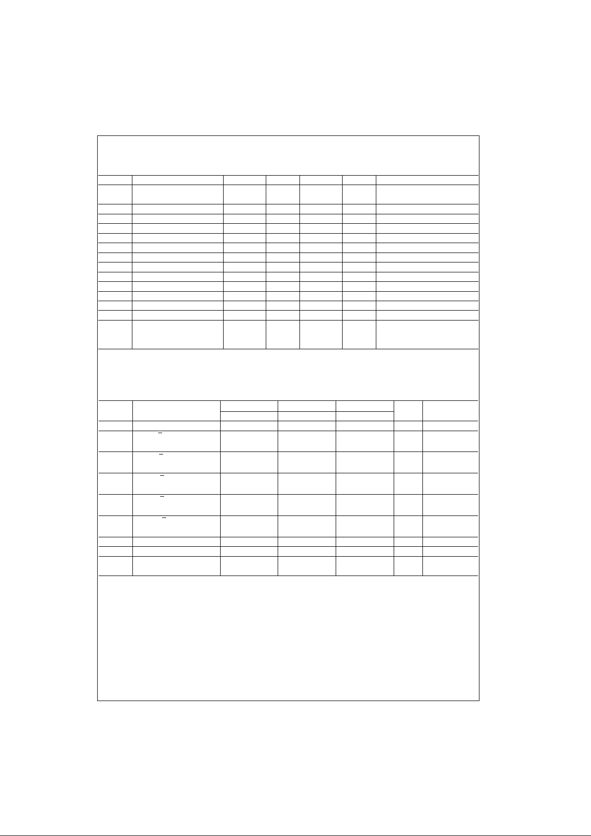
TTL-to-ECL DC Electrical Characteristics
(Note 9)
V
EE
= −4.2V to −5.7V, GND = 0V, TC = 0°C to +85°C, V
TTL
= +4.5V to +5.5V
Note 8: Either voltage limit or cu rrent limit is sufficient to protec t inputs.
Note 9: The specified limits represent the “worst case” value for the parameter. Since these values normally occur at the temperature extremes, additional
noise immunity and guardbanding can be achieved by decreasing the all owable syste m opera ti ng r ange s. Co ndi ti ons fo r t est ing shown in the ta ble s are chosen to guarantee operation under “worst case” conditions.
Storage Temperature (T
STG
) −65°C to +150°C
Maximum Junction Temperature
(T
J
) +150°C
V
EE
Pin Potential to Ground Pin −7.0V to +0.5V
V
TTL
Pin Potential to Ground Pin −0.5V to +6.0V
ECL Input Voltage (DC) V
EE
to +0.5V
ECL Output Current
(DC Output HIGH)
−50 mA
TTL Input Voltage (Note 6)
−0.5V to +7.0V
TTL Input Current (Note 6)
−30 mA to +5.0 mA
Voltage Applied to Output in
HIGH State 3-STATE Output
−0.5V to +5.5V
Current Applied to TTL
Output in LOW State (Max) twice the Rated I
OL
(mA)
ESD (Note 7)
≥ 2000V
Case Temperature (T
C
)
Commercial 0
°C to +85°C
Industrial
−40°C to +85°C
ECL Supply Voltage (V
EE
) −5.7V to −4.2V
TTL Supply Voltage (V
TTL
) +4.5V to +5.5V
Symbol Parameter Min Typ Max Units Conditions
V
OH
Output HIGH Voltage −1025 −955 −870 mV VIN = V
IH(Max)
or V
IL(Min)
V
OL
Output LOW Voltage −1830 −1705 −1620 mV Loading with 50Ω to − 2V
Cutoff Voltage −2000 −1950 mV OE and LE LOW, DIR HIGH
V
IN
= V
IH(Max)
or VIL(Min),
Loading with 50Ω to −2V
V
OHC
Output HIGH Voltage
−1035 mV
Corner Point High VIN = V
IH(Min)
or V
IL(Max)
V
OLC
Output LOW Voltage
−1610 mV
Loading with 50Ω to −2V
Corner Point Low
V
IH
Input HIGH Voltage 2.0 5.0 V Over V
TTL
, VEE, TC Range
V
IL
Input LOW Voltage 0 0.8 V Over V
TTL
, VEE, TC Range
I
IH
Input HIGH Current 5.0 µAVIN = +2.7V
Breakdown Test 0.5 mA VIN = +5.5V
I
IL
Input LOW Current −700 µAVIN = +0.5V
V
FCD
Input Clamp
−1.2 V IIN = −18 mA
Diode Voltage
I
EE
VEE Supply Current −99 −50 mA LE LOW, OE and DIR HIGH
Inputs Open
I
EEZ
VEE Supply Current −159 −90 mA LE and OE LOW, DIR HIGH
Inputs Open
Page 5
5 www.fairchildsemi.com
100398
Commercial Version (Continued)
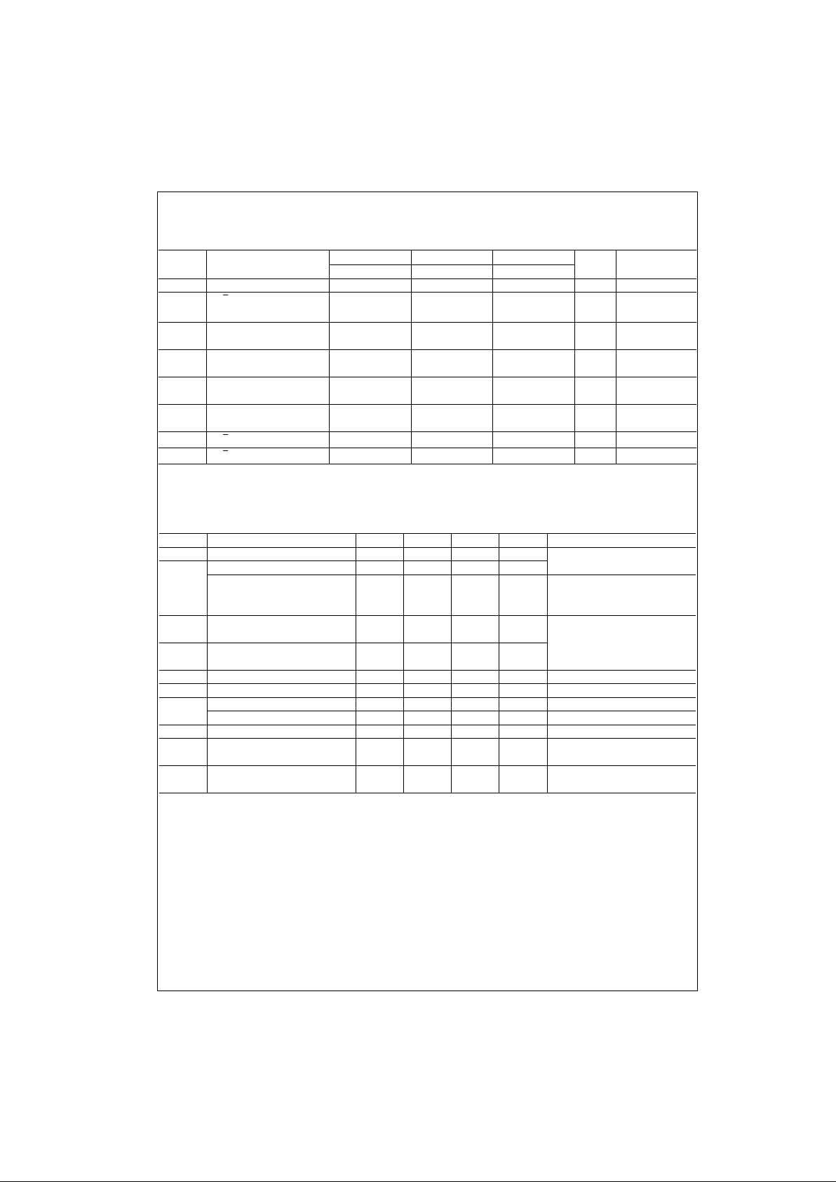
ECL-to-TTL DC Electrical Characteristi cs (Note 10)
VEE = −4.2V to −5.7V, GND = 0V, TC = 0°C to +85°C, CL = 50 pF, V
TTL
= +4.5V to +5.5V
Note 10: The specified lim it s represent the “worst case” valu e f or the parameter. Since th es e values normally o c cu r at the temperature extremes, additio nal
noise immunity and guardbanding can be achieved by decreasin g the al l owable syste m opera ti ng ran ge s. Cond it i ons fo r t estin g sho w n in the tabl es are chosen to guarantee operation under “worst case” conditions.
DIP and PCC TTL-to-ECL AC Electrical Characteristics
VEE = −4.2V to −5.7V, V
TTL
= +4.5V to +5.5V
Symbol Parameter Min Typ Max Units Conditions
V
OH
Output HIGH Voltage 2.7 3.1 V IOH = −3 mA, V
TTL
= 4.75V
2.4 2.9 V I
OH
= −3 mA, V
TTL
= 4.50V
V
OL
Output LOW Voltage 0.3 0.5 V IOL = 24 mA, V
TTL
= 4.50V
V
IH
Input HIGH Voltage −1165 −870 mV Guaranteed HIGH Signal for All Inputs
V
IL
Input LOW Voltage −1830 −1475 mV Guaranteed LOW Signal for All Inputs
V
DIFF
Input Voltage Differential 150 mV Required for Full Output Swing
V
CM
Common Mode Voltage GNDECL − 2.0 GNDECL − 0.5 V
I
IH
Input HIGH Current 30 µAVIN = VIH (Max)
I
IL
Input LOW Current 0.50 µAVIN = VIL (Min)
I
OZHT
3-STATE Current Output High 70 µAV
OUT
= +2.7V
I
OZLT
3-STATE Current Output Low −650 µAV
OUT
= +0.5V
I
OS
Output Short-Circuit Current −100 −225 mA V
OUT
= 0.0V, V
TTL
= +5.5V
I
CEX
Output HIGH Leakage Current 50 µAV
OUT
= 5.5V
I
ZZ
Bus Drainage Test 500 µAV
OUT
= 5.25V
I
TTL
V
TTL
Supply Current 39 mA TTL Outputs LOW
27 mA TTL Outputs HIGH
39 mA TTL Outputs in 3-STATE
Symbol Parameter
T
C
= 0°CT
C
= 25°CT
C
= 85°C
Units Conditions
Min Max Min Max Min Max
f
MAX
Toggle Frequency 180 180 180 MHz
t
PLH
Tn to En, E
n
0.90 2.10 0.80 2.20 0.70 2.50 ns Figures 1, 3
t
PHL
(Transparent)
t
PLH
LE to En, E
n
1.40 2.70 1.50 2.70 1.80 3.10 ns Figures 1, 3
t
PHL
t
PZH
OE to En, E
n
2.90 8.00 2.80 6.90 2.80 5.80 ns Figures 1, 3
(Cutoff to HIGH)
t
PHZ
OE to En, E
n
1.30 2.70 1.40 2.90 1.70 3.40 ns Figures 1, 3
(HIGH to Cutoff)
t
PHZ
DIR to En, E
n
1.30 2.70 1.40 2.90 1.80 3.50 ns Figures 1, 3
(HIGH to Cutoff)
t
S
Tn to LE 0.70 0.70 0.70 ns Figures 1, 3
t
H
Tn to LE 0.90 0.80 0.70 ns Figures 1, 3
t
TLH
Transition Time
0.45 1.50 0.45 1.50 0.45 1.50 ns Figures 1, 3
t
THL
20% to 80%, 80% to 20%
Page 6
www.fairchildsemi.com 6
100398
Commercial Version (Continued)
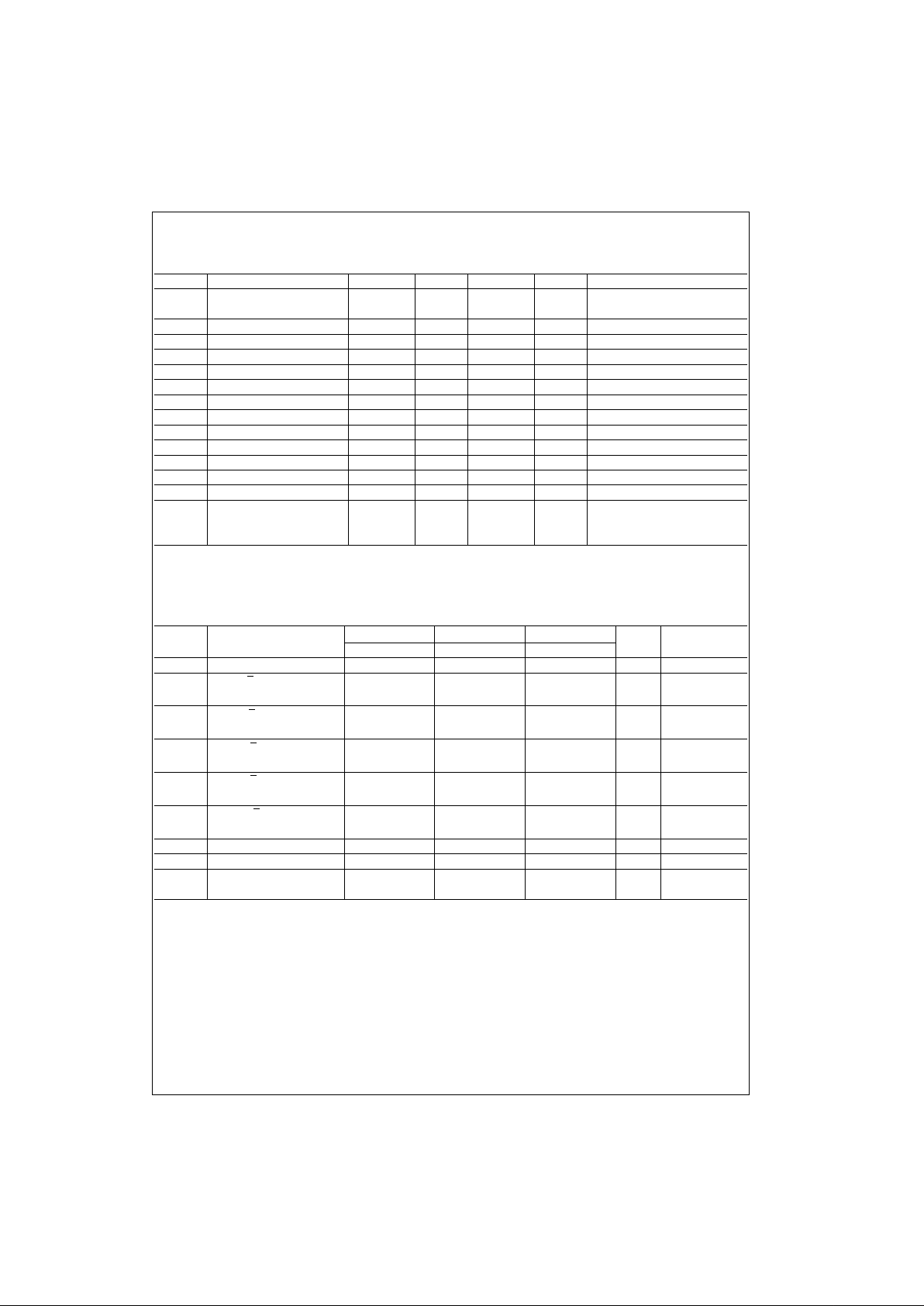
DIP and PCC ECL-to-TTL AC Electrical Characteristics
VEE = −4.2V to −5.7V, V
TTL
= +4.5V to +5.5V, CL = 50 pF
Industrial Version
TTL-to-ECL DC Electrical Characteristics
VEE = −4.2V to −5.7V, GND = 0V, TC = −40°C to +85°C, V
TTL
= +4.5V to +5.5V (Note 11)
Note 11: The specified limits represent the “worst case” value fo r t he parameter. Since thes e values normally oc c ur at the temperature extremes, addit ional
noise immunity and guardbanding can be achieved by decreasing the all owable syste m opera ti ng r ange s. Co ndi ti ons fo r t est ing shown in the ta ble s are cho-
sen to guarantee operation under “worst case” conditions.
Symbol Parameter
T
C
= 0°CT
C
= 25°CT
C
= 85°C
Units Conditions
Min Max Min Max Min Max
f
MAX
Toggle Frequency 75 75 75 MHz
t
PLH
En, En to T
n
1.70 4.90 1.70 5.10 1.80 5.80 ns Figures 2, 4
t
PHL
(Transparent)
t
PLH
LE to T
n
2.30 4.60 2.40 4.70 2.60 4.90
ns Figures 2, 4
t
PHL
3.30 5.50 3.50 5.70 4.00 6.70
t
PZH
OE to T
n
2.30 4.90 2.10 4.70 2.00 4.30
ns Figures 2, 5
t
PZL
(Enable Time) 4.10 7.90 4.10 7.80 4.20 7.80
t
PHZ
OE to T
n
3.30 7.90 3.30 7.50 3.70 7.90
ns Figures 2, 5
t
PLZ
(Disable Time) 4.10 7.50 4.30 7.80 5.30 9.40
t
PHZ
DIR to T
n
2.00 6.00 1.90 5.70 1.70 5.20
ns Figures 2, 6
t
PLZ
(Disable Time) 2.00 4.00 2.00 3.70 1.90 3.70
t
S
En, En to LE 0.50 0.50 0.50 ns Figures 2, 4
t
H
En, En to LE 1.00 1.00 1.00 ns Figures 2, 4
Symbol Parameter Min Typ Max Units Con ditions
V
OH
Output HIGH Voltage −1085 −955 −870 mV VIN = V
IH(Max)
or V
IL(Min)
V
OL
Output LOW Voltage −1830 −1705 −1575 mV Loading with 50Ω to −2V
Cutoff Voltage OE and LE Low, DIR High
−2000 −1900 mV VIN= V
IH(Max)
or V
IL(Min)
,
Loading with 50Ω to −2V
V
OHC
Output HIGH Voltage
−1095 mV
Corner Point HIGH V
IN
= V
IH(Min)
or V
IL(Max)
V
OLC
Output LOW Voltage
−1565 mV
Loading with 50Ω to −2V
Corner Point LOW
V
IH
Input HIGH Voltage 2.0 5.0 V Over V
TTL
, VEE, TC Range
V
IL
Input LOW Voltage 0 0.8 V Over V
TTL
, VEE, TC Range
I
IH
Input HIGH Current 5.0 µAVIN = +2.7V
Breakdown Test 0.5 mA V
IN
= +5.5V
I
IL
Input LOW Current −700 µAVIN = +0.5V
V
FCD
Input Clamp
−1.2 V IIN = −18 mA
Diode Voltage
I
EE
VEE Supply Current −99 −40 mA LE Low, OE and DIR High
Inputs Open
Page 7
7 www.fairchildsemi.com
100398
Industrial Version (Con tinu ed)
ECL-to-TTL DC Electrical Characteristi cs (Note 12)
VEE = −4.2V to −5.7V, GND = 0V, TC = −40°C to +85°C, CL = 50 pF, V
TTL
= +4.5V to +5.5V
Note 12: The specified lim it s represent the “worst case” valu e f or the parameter. Since th es e values normally o c cu r at the temperature extremes, additio nal
noise immunity and guardbanding can be achieved by decreasin g the al l owable syste m opera ti ng ran ge s. Cond it i ons fo r t estin g sho w n in the tabl es are chosen to guarantee operation under “worst case” conditions.
PCC TTL-to-ECL AC Electrical Characteristics
VEE = −4.2V to −5.7V, V
TTL
= +4.5V to +5.5V
Symbol Parameter Min Typ Max Units Conditions
V
OH
Output HIGH Voltage 2.7 3.1 V IOH = −3 mA, V
TTL
= 4.75V
2.4 2.9 V I
OH
= −3 mA, V
TTL
= 4.50V
V
OL
Output LOW Voltage 0.3 0.5 V IOL = 24 mA, V
TTL
= 4.50V
V
IH
Input HIGH Voltage −1170 −870 mV Guaranteed HIGH Signal for All Inputs
V
IL
Input LOW Voltage −1830 −1480 mV Guaranteed LOW Signal for All Inputs
V
DIFF
Input Voltage Differential 150 mV Required for Full Output Swing
V
CM
Common Mode Voltage GNDECL − 2.0 GNDECL − 0.5 V
I
IH
Input HIGH Current 35 µAVIN = V
IH(Max)
I
IL
Input LOW Current 0.50 µAVIN = V
IH(Min)
I
OZHT
3-STATE Current Output High 70 µAV
OUT
= +2.7V
I
OZLT
3-STATE Current Output Low −650 µAV
OUT
= +0.5V
I
OS
Output Short-Circuit Current −100 −225 mA V
OUT
= 0.0V, V
TTL
= +5.5V
I
CEX
Output HIGH Leakage Current 50 µAV
OUT
= 5.5V
I
ZZ
Bus Drainage Test 500 µAV
OUT
= 5.25V
I
TTL
V
TTL
Supply Current 39 mA TTL Outputs LOW
27 mA TTL Outputs HIGH
39 mA TTL Outputs in 3-STATE
Symbol Parameter
T
C
= −40°CT
C
= +25°CT
C
= +85°C
Units Conditions
Min Max Min Max Min Max
f
MAX
Toggle Frequency 180 180 180 MHz
t
PLH
Tn to En, E
n
0.90 2.40 0.80 2.20 0.70 2.50 ns Figures 1, 3
t
PHL
(Transparent)
t
PLH
LE to En, E
n
1.30 2.70 1.50 2.70 1.80 3.10 ns Figures 1, 3
t
PHL
t
PZH
OE to En, E
n
2.90 9.00 2.80 6.90 2.80 5.80 ns Figures 1, 3
(Cutoff to HIGH)
t
PHZ
OE to En, E
n
1.10 2.70 1.40 2.90 1.70 3.40 ns Figures 1, 3
(HIGH to Cutoff)
t
PHZ
DIR to En, E
n
1.10 2.70 1.40 2.90 1.80 3.50 ns Figures 1, 3
(HIGH to Cutoff)
t
S
Tn to LE 0.70 0.70 0.70 ns Figures 1, 3
t
H
Tn to LE 0.90 0.90 0.90 ns Figures 1, 3
t
TLH
Transition Time
0.45 2.20 0.45 1.50 0.45 1.50 ns Figures 1, 3
t
THL
20% to 80%, 80% to 20%
Page 8
www.fairchildsemi.com 8
100398
Industrial Version (Continued)
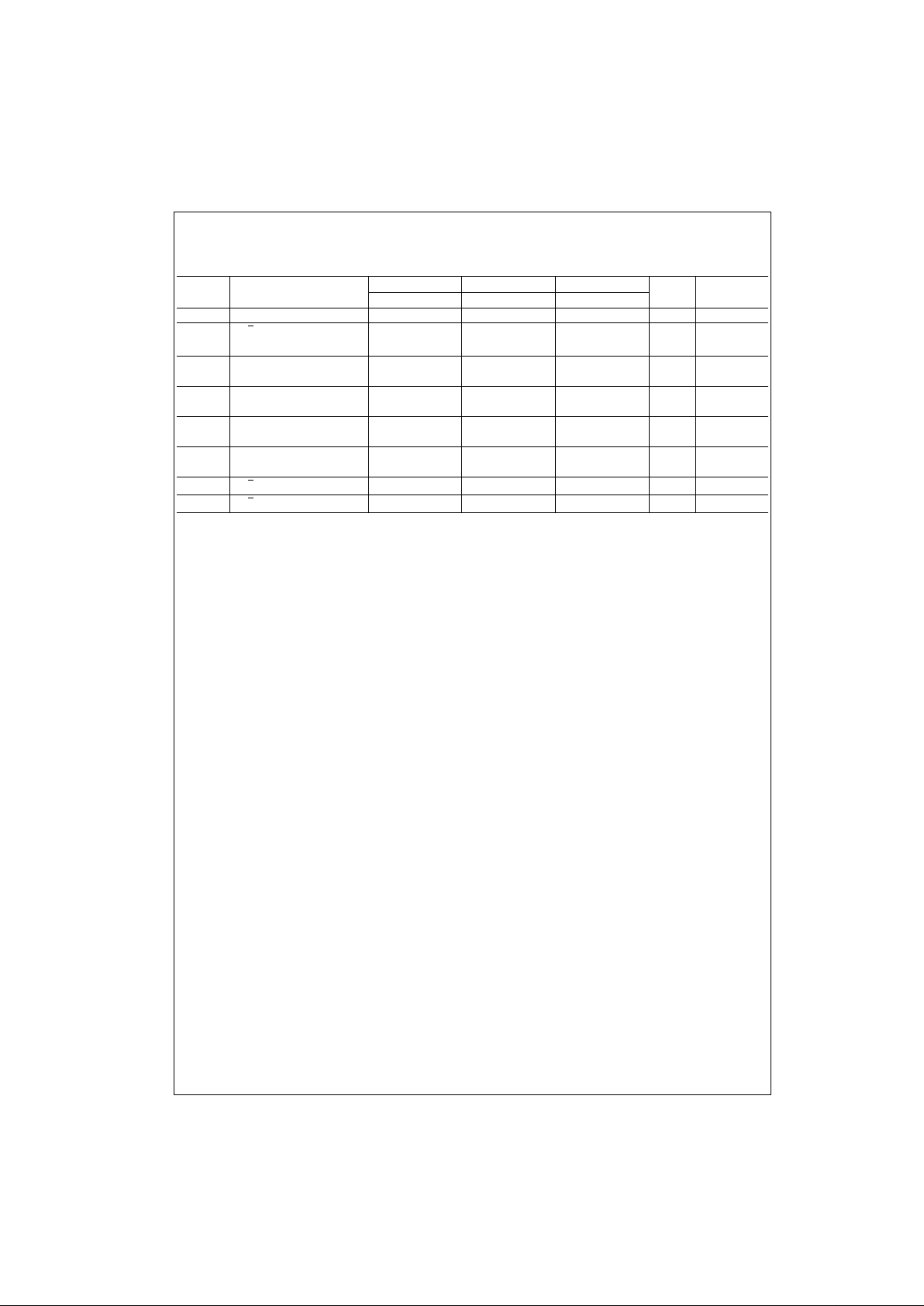
PCC ECL-to-TTL AC Electrical Characteristics
VEE = −4.2V to −5.7V, V
TTL
= +4.5V to +5.5V, CL = 50 pF
Symbol Parameter
TC = −40°CT
C
= +25°CT
C
= +85°C
Units Conditions
MinMaxMinMaxMinMax
f
MAX
Toggle Frequency 75 75 75 MHz
t
PLH
En, En to T
n
1.70 4.90 1.70 5.10 1.80 5.80 ns Figures 2, 4
t
PHL
(Transparent)
t
PLH
LE to T
n
2.30 4.80 2.40 4.70 2.60 4.90
ns Figures 2, 4
t
PHL
3.30 5.50 3.50 5.70 4.00 6.70
t
PZH
OE to T
n
2.30 5.50 2.10 4.70 2.00 4.30
ns Figures 2, 5
t
PZL
(Enable Time) 4.10 8.20 4.10 7.80 4.20 7.80
t
PHZ
OE to T
n
3.20 7.90 3.30 7.50 3.70 7.90
ns Figures 2, 5
t
PLZ
(Disable Time) 4.00 7.40 4.30 7.80 5.30 9.40
t
PHZ
DIR to T
n
2.00 6.60 1.90 5.70 1.70 5.20
ns Figures 2, 6
t
PLZ
(Disable Time) 2.10 4.70 2.00 3.70 1.90 3.70
t
S
En, En to LE 0.50 0.50 0.50 ns Figures 2, 4
t
H
En, En to LE 1.00 1.00 1.00 ns Figures 2, 4
Page 9
9 www.fairchildsemi.com
100398
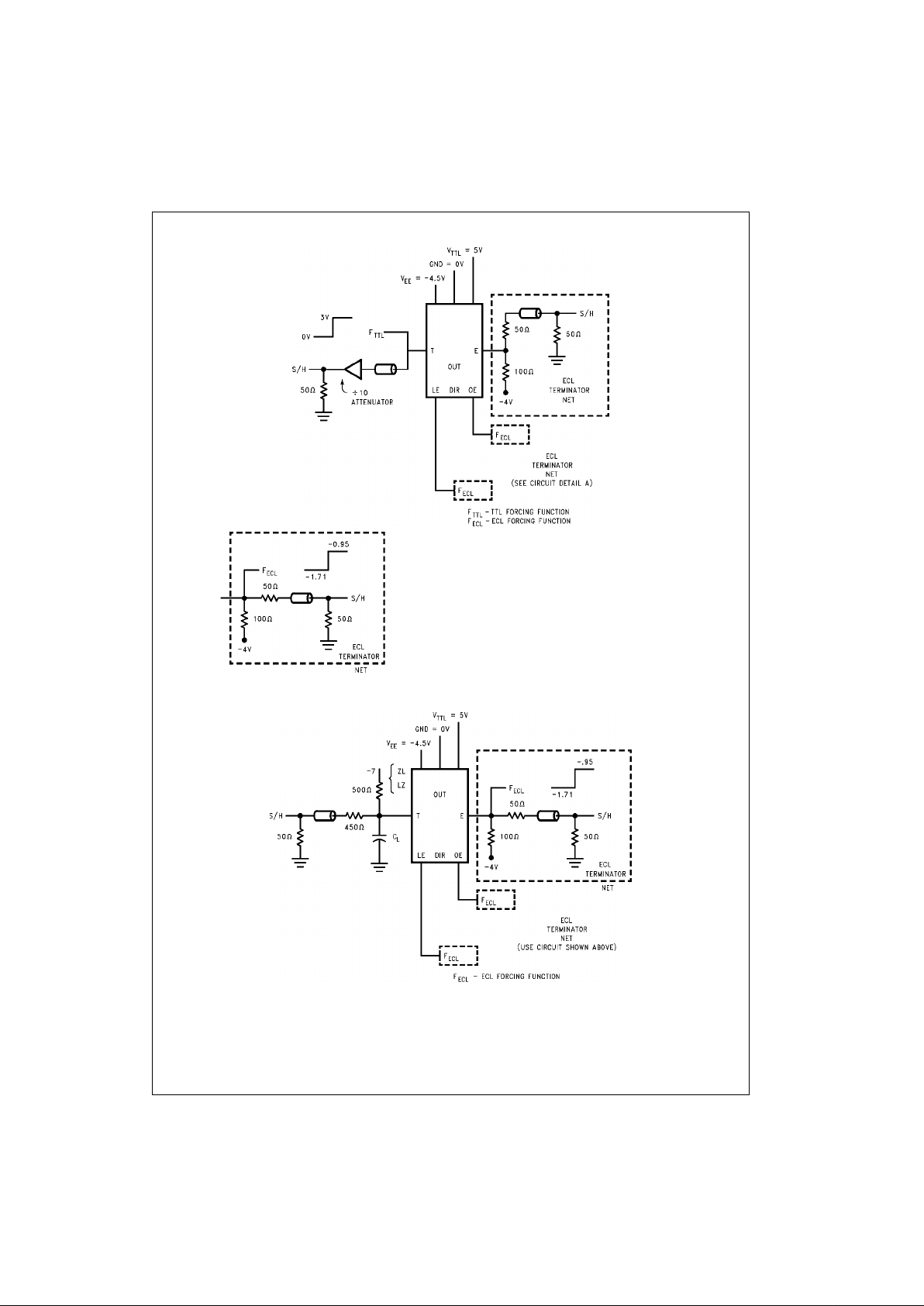
Test Circuitry
FIGURE 1. TTL-to-ECL AC Test Circuit
CL = 50 pF including str ay and jig capacitance.
Note: 50Ω to ground termination must be included on ECL I/O pins not monitored by a 50Ω scope to prevent oscillatory feedback.
FIGURE 2. ECL-to-TTL AC Test Circuit
Page 10
www.fairchildsemi.com 10
100398
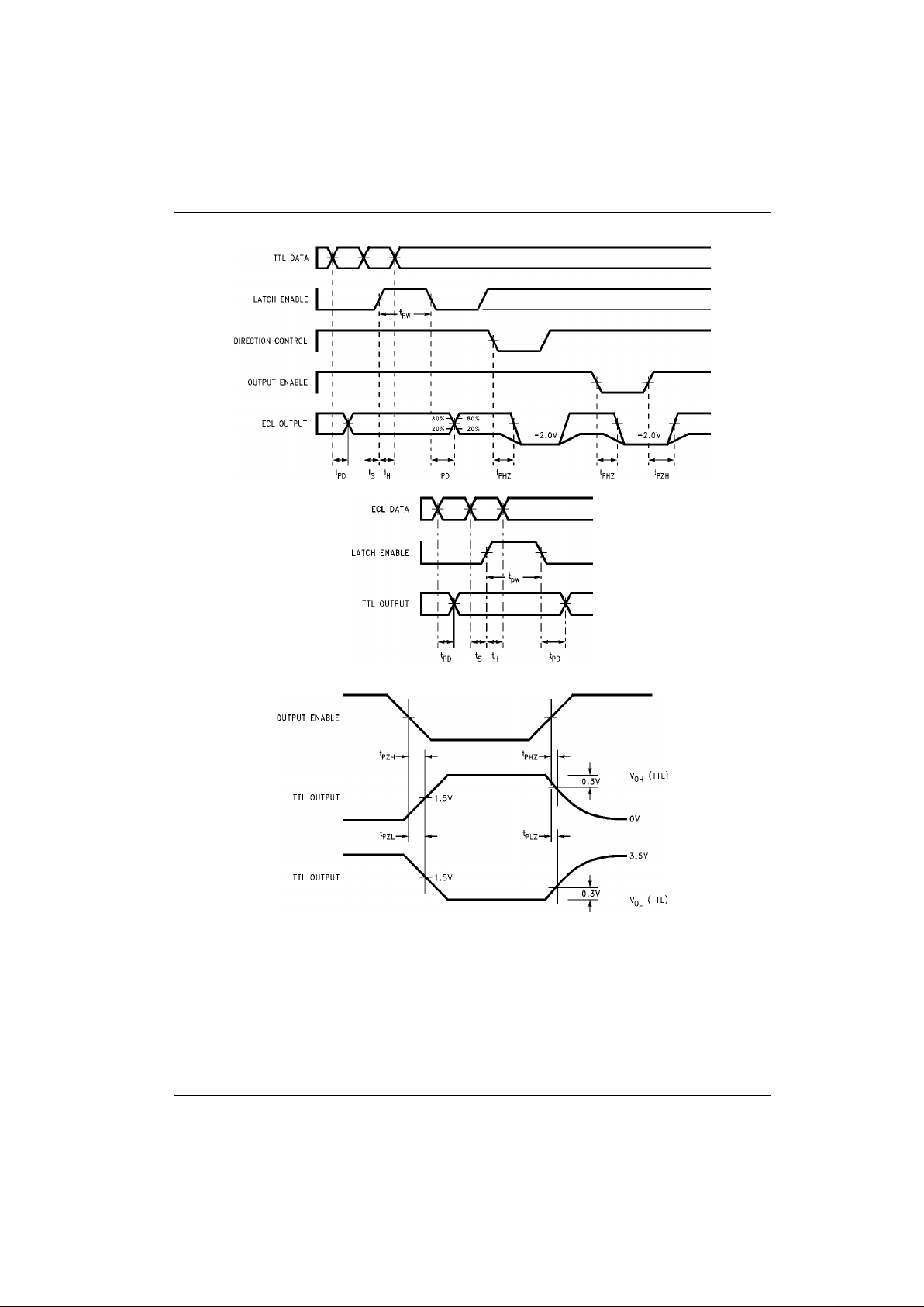
Switching Waveforms
FIGURE 3. TTL-to-ECL Transition—Propagation Delay and Transition Times
Note: DIR is LOW, and OE is HIGH
FIGURE 4. ECL-to-TTL Transition—Propagation Delay and Transition Times
Note: DIR is LOW, LE is HIGH
FIGURE 5. ECL-to-TTL Transition, OE to TTL O u tput, Enable and Disable Times
Page 11
11 www.fairchildsemi.com
100398
Switching Waveforms (Continued)
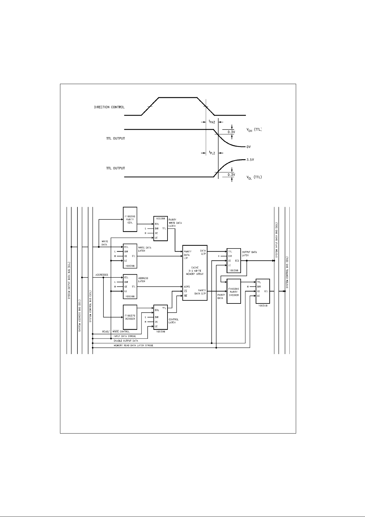
Note: OE is HIGH, LE is HIGH
FIGURE 6. ECL-to-TTL Transition, DIR to TTL Output, Disable Time
Applications
FIGURE 7. Applications Diagram—MOS/TTL SRAM Interface Using 100398 ECL–TTL Latched Translator
Page 12
www.fairchildsemi.com 12
100398
Physical Dimensions inches (millimeters) unless otherwise noted
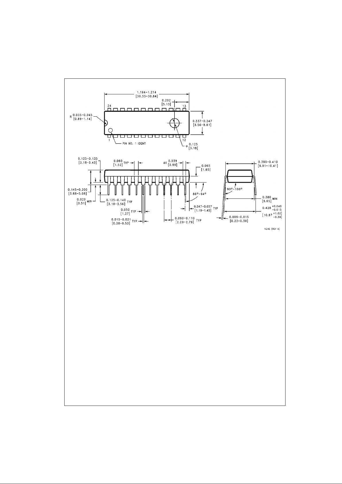
24-Lead Plastic Dual-In-Line Package (PDIP), JEDEC MS-010, 0.400 Wide
Package Number N24E
Page 13
13 www.fairchildsemi.com
100398 Quad Differential ECL/TTL Translating Transceiver with Latch
Physical Dimensions inches (millimeters) unless otherwise noted (Continued)
28-Lead Plastic Lead Chip Carrier (PLCC), JEDEC MO-047, 0.450 Square
Package Number V28A
Fairchild does not assume any responsibility for use of any circuitry described , no circuit patent licenses are implied and
Fairchild reserves the right at any time without notice to change said circuitry and specifications.
LIFE SUPPORT POLICY
FAIRCHILD’S PRODUCTS ARE NOT AUTHORIZED FOR USE AS CRITICAL COMPONENTS IN LIFE SUPPORT
DEVICES OR SYSTEMS WITHOUT THE EXPRESS WRITTEN APPROVAL OF THE PRESIDENT OF FAIRCHILD
SEMICONDUCTOR CORPORATION. As used herein:
1. Life support devices or systems are devices or syste ms
which, (a) are intended for surgical implant into the
body, or (b) support or sustain life, and (c) whose failure
to perform when properly used in accordance with
instructions for use provide d in the labe l ing, can be re asonably expected to result in a significant injury to the
user.
2. A critical component in any compo nent o f a li fe supp ort
device or system whose failure to perform can be reasonably expected to cause the failure of the l ife support
device or system, or to affect its safety or effectiveness.
www.fairchildsemi.com
 Loading...