

Datasheet 100391SCX, 100391SC, 100391QIX, 100391QI, 100391QCX Datasheet (Fairchild Semiconductor)
...Page 1
© 2000 Fairchild Semiconductor Corporation DS010939 www.fairchildsemi.com
July 1992
Revised August 2000
100391 Low Power Single Supply Hex TTL-to-PECL Translator
100391
Low Power Single Supply Hex TTL-to-PECL Translator
General Description
The 100391 is a hex translator for converting TTL logic levels to F100K PECL logic levels. The unique feature of this
translator, is the ability to do this translation using only one
+5V supply. The differential outputs allow each circuit to be
used as an inverting/non-i nvert ing tr anslator, or as a differential line driver. A common enable (E), whe n LOW, holds
all inverting outputs HIGH and all non-inverting inputs
LOW.
The 100391 is ideal fo r those mixed PECL/TTL applications which only have
+5V supply available . When use d in
the differential mode, the 10 0391, due to its hi gh common
mode rejection, overco mes voltag e gradients be tween the
TTL and PECL ground systems.
Features
■ Operates from a single +5V supply
■ Differential PECL outputs
■ 2000V ESD protection
■ Companion chip to 100390 hex PECL-to-TTL translator
Ordering Code:
Devices also availab le in Tape and Reel. Specify by appending th e s uffix let t er “X” to the ordering code.
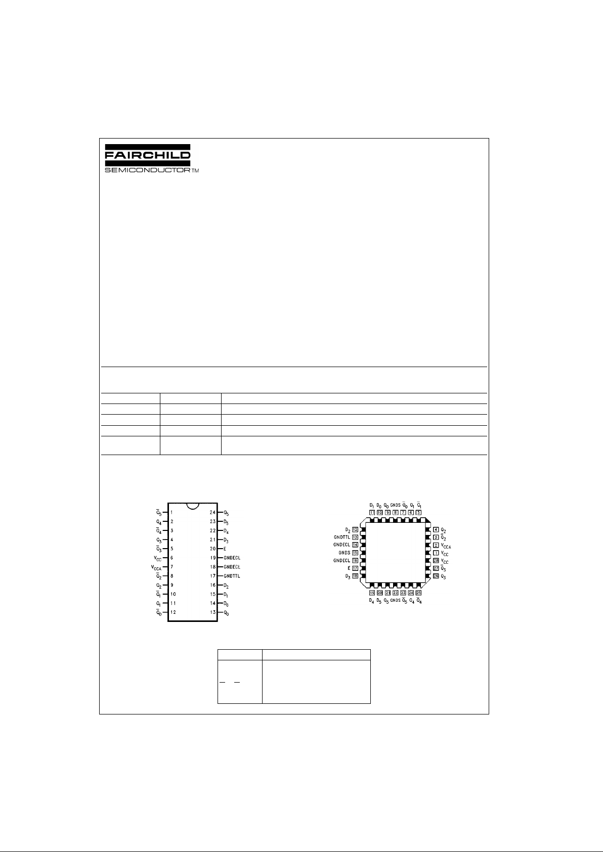
Connection Diagrams
24-Pin DIP and SOIC 28-Pin PLCC
Pin Descriptions
Order Number Package Number Package Description
100391SC M24B 24-Lead Small Outline Integrated Circuit (SOIC), JEDEC MS-013, 0.300 Wide
100391PC N24E 24-Lead Plastic Dual-In-Line Package (PDIP), JEDEC MS-010, 0.400 Wide
100391QC V28A 28-Lead Plastic Lead Chip Carrier (PLCC), JEDEC MO-047, 0.450 Square
100391QI V28A 28-Lead Plastic Lead Chip Carrier (PLCC), JEDEC MO-047, 0.450 Square
Industrial Temperature Range (
−40°C to +85°C)
Pin Names Description
D
0
- D
5
Data Inputs (TTL)
Q
0
- Q
5
Data Outputs (PECL)
Q
0
- Q
5
Inverting Data Outputs (PECL)
E Enable Input (TTL)
Page 2
www.fairchildsemi.com 2
100391
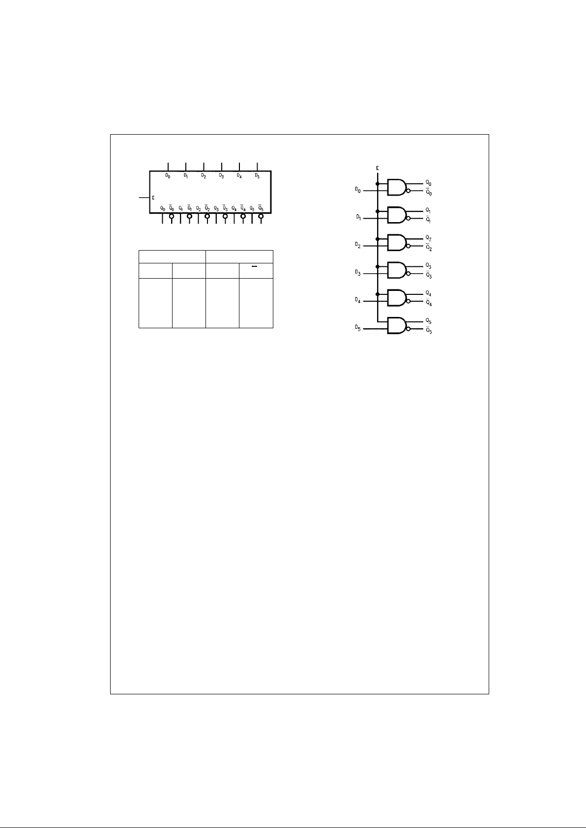
Logic Symbol
Truth Table
H = HIGH Voltage Level
L = LOW Voltage Level
Logic Diagram
Inputs Outputs
D
n
E
Q
n
Q
n
HHHL
LHLH
HLLH
LLLH
Page 3
3 www.fairchildsemi.com
100391
Absolute Maximum Ratings(Note 1) Recommended Operating
Conditions
Note 1: The “Absolute Maximum Ratings” are those value s beyond which
the safety of the dev ice cannot b e guaranteed . The device sh ould not be
operated at these limit s. The parametric values defi ned in the Electrical
Characteristics tables are not guaranteed at the absolute maximum rating.
The “Recomm ended O peratin g Cond itions ” table will defin e the condition s
for actual device operation.
Note 2: Either voltage lim it or c urrent limit is sufficient to pro te c t in puts.
Note 3: ESD testing conforms to MIL-STD-883, Method 3015.
Commercial Version
TTL-to-PECL DC Electrical Characteris tics
(Note 4)
V
CC
= +5.0V ± 10%, GND = 0V, T
C
= 0°C to +85°C
Note 4: The specified limits represent the “worst case” value for the parameter. Since these values normally occur at the temperature extremes, additional
noise immunity and guardbanding can be achieved by decreasin g the al l owable syste m opera ti ng ran ge s. Cond it i ons fo r t estin g sho w n in the tabl es are chosen to guarantee operation under “worst case” conditions.
PDIP AC Electrical Characteristics
VCC = 5.0V ± 10%
Storage Temperature (T
STG
) −65°C to +150°C
Maximum Junction Temperature (T
J
) +150°C
Pin Potential to Ground Pin (V
CC
) −0.5V to +7.0V
PECL Output Current
(DC Output HIGH)
−50 mA
TTL Input Voltage (Note 2)
−0.5V to +7.0V
TTL Input Current (Note 2)
−30 mA to + 5.0 mA
ESD (Last Passing Voltage)
(Note 3)
≥2000V
Case Temperature (T
C
)
Industrial
−40°C to +85°C
Commercial 0
°C to +85°C
Supply Voltage (V
CC
) 4.5V to 5.5V
Symbol Parameter Min Typ Max Units Conditions
V
OH
Output HIGH Voltage VCC− 1025 VCC− 955 VCC− 870 mV VIN = V
IH(max)
or V
IL (min)
V
OL
Output LOW Voltage VCC− 1890 VCC − 1705 VCC − 1620 mV Loading with 50Ω to VCC − 2V
V
OHC
Output HIGH Voltage
VCC − 1035 mV
Corner Point High VIN = V
IH(min)
or V
IL (max)
V
OLC
Output LOW Voltage
VCC − 1610 mV
Loading with 50Ω to VCC − 2V
Corner Point Low
V
IH
Input HIGH Voltage 2.0 5.0 V Over V
TTL
, VEE, TC Range
V
IL
Input LOW Voltage 0 0.8 V Over V
TTL
, VEE, TC Range
I
IH
Input LOW Current 10 µAVIN = +2.7V
Breakdown Test 20 µAV
IN
= +5.5V
I
IL
Input LOW Current
mA VIN = +0.5VDn −0.8
E −4.2
V
FCD
Input Clamp
−1.2 V I
IN
= −18 mA
Diode Voltage
I
CC
VCC Supply Current 32 69 mA Inputs OPEN
Symbol Parameter
T
C
= 0°CT
C
= +25°CT
C
= +85°C
Units Conditions
Min Max Min Max Min Max
t
PLH
Propagation Delay
0.30 1.40 0.35 1.30 0.40 1.30 ns Figures 1, 2
t
PHL
Data to Output
t
PLH
Propagation Delay
0.40 1.50 0.45 1.40 0.50 1.40 ns Figures 1, 2
t
PHL
Enable to Output
t
TLH
Transition Time
0.35 1.70 0.35 1.70 0.35 1.70 ns Figures 1, 2
t
THL
20% to 80%, 80% to 20%
Page 4

www.fairchildsemi.com 4
100391
Commercial Version (Continued)
SOIC and PLCC AC Electrical Characteristics
VCC = 5.0V ± 10%
Note 5: Output-to-Output Skew is defined as the absolute value of the difference between the actual propagation delay for any outputs within the same packaged device. The spe cificatio ns apply to any ou tputs switch ing in the sam e direction either HIGH-t o-LOW (t
OSHL
) or LOW-to-HIGH (t
OSLH
), or in opposite
directions both HL and LH (t
OST
). Parameters t
OST
and tPS guaranteed by design.
Symbol Parameter
T
C
= 0°CT
C
= +25°CT
C
= +85°C
Units Conditions
Min Max Min Max Min Max
t
PLH
Propagation Delay
0.30 1.40 0.35 1.30 0.40 1.30 ns
Figures 1, 2
t
PHL
Data to Output
t
PLH
Propagation Delay
0.40 1.50 0.45 1.40 0.50 1.40 ns
t
PHL
Enable to Output
t
TLH
Transition Time
0.35 1.70 0.35 1.70 0.35 1.70 ns
t
THL
20% to 80%, 80% to 20%
t
OSHL
Maximum Skew Common Edge
750 750 750 ps
PLCC Only
(Note 5)
Output-to-Output Variation
Data to Output Path
t
OSLH
Maximum Skew Common Edge
700 700 700 ps
PLCC Only
(Note 5)
Output-to-Output Variation
Data to Output Path
t
OST
Maximum Skew Opposite Edge
450 450 450 ps
PLCC Only
(Note 5)
Output-to-Output Variation
Data to Output Path
t
PS
Maximum Skew
525 525 525 ps
PLCC Only
(Note 5)
Pin (Signal) Transition Variation
Data to Output Path
Page 5

5 www.fairchildsemi.com
100391
Industrial Version
PLCC DC Electrical Characteristics
(Note 6)
VCC = +5.0V ± 10%, GND = 0V
Note 6: The specified limits represent the “worst case” value for the parameter. Since these values normally occur at the temperature extremes, additional
noise immunity and guardbanding can be achieved by decreasin g the al l owable syste m opera ti ng ran ge s. Cond it i ons fo r t estin g sho w n in the tabl es are chosen to guarantee operation under “worst case” conditions.
PLCC AC Electrical Characteristics
VCC = +5.0V ± 10%, GND = 0V
Symbol Parameter
T
C
= −40°CT
C
= 0°C to +85°C
Units Conditions
MinMaxMinMax
V
OH
Output HIGH Voltage VCC− 1085 VCC − 870 VCC − 1025 VCC − 870 mV VIN = V
IH(max)
or V
IL (min)
V
OL
Output LOW Voltage VCC − 1830 VCC − 1575 VCC − 1830 VCC − 1620 mV Loading with 50Ω to VCC − 2V
V
OHC
Output HIGH Voltage VCC − 1095 VCC − 1035 mV VIN = V
IH(min)
or V
IL(max)
Loading with 50Ω to VCC − 2V
V
OLC
Output LOW Voltage VCC − 1565 VCC − 1610 mV
V
IH
Input HIGH Voltage 2.0 5.0 2.0 5.0 V
V
IL
Input LOW Voltage 0 0.8 0 0.8 V
V
IH
Input HIGH Current 10 10 µAVIN = +2.7V
Breakdown Test 20 20 µAVIN = +5.5V
I
IL
Input LOW Current
mV VIN = +0.5VD
n
−0.8 −0.8
E −4.2 −4.2
V
FCD
Input Clamp
−1.2 −1.2 V IIN = −18 mA
Diode Voltage
I
CC
VCC Supply Current 29 69 29 69 mA Inputs OPEN
Symbol Parameter
TC = −40°CT
C
= +25°CT
C
= +85°C
Units Conditions
Min Max Min Max Min Max
t
PLH
Propagation Delay
0.20 1.50 0.35 1.30 0.40 1.30 ns
Figures 1, 2
t
PHL
Data to Output
t
PLH
Propagation Delay
0.35 1.60 0.45 1.40 0.50 1.40 ns
t
PHL
Enable to Output
t
TLH
Transition Time
0.35 1.70 0.35 1.70 0.35 1.70 ns
t
THL
20% to 80%, 80% to 20%
Page 6

www.fairchildsemi.com 6
100391
Switching Waveforms
FIGURE 1. Propagation Delay, Cut-Off and Transition Times
Test Circuit
FIGURE 2. AC Test Circuit
Notes:
V
CC
= V
CCA
= +2V, GNDPECL = GNGTTL = 30.V
V
IH
= 0V, VIL = −3V
L1, L2 and L3
= equal length 50Ω impedance lines
R
T
= 50Ω terminator internal to scope
Decoupling 0.1
µF from GND to V
CC
, VEE and V
TTL
All unused outputs are loaded with 50Ω to GND
C
L
= Fixture and stray capacitance ≤ 3 pF
Page 7

7 www.fairchildsemi.com
100391
Physical Dimensions inches (millimeters) unless otherwise noted
28-Lead Small Outline Integrated Circuit (SOIC), JEDEC MS-013, 0.300 Wide
Package Number M24B
24-Lead Plastic Dual-In-Line Package (PDIP), JEDEC MS-010, 0.400 Wide
Package Number N24E
Page 8

www.fairchildsemi.com 8
100391 Low Power Single Supply Hex TTL-to-PECL Translator
Physical Dimensions inches (millimeters) unless otherwise noted (Continued)
28-Lead Plastic Lead Chip Carrier (PLCC), JEDEC MO-047, 0.450 Square
Package Number V28A
Fairchild does not assume any responsibility for use of any circuitr y described, no circuit patent licenses are implied and
Fairchild reserves the right at any time without notice to change said circuitry and specifications.
LIFE SUPPORT POLICY
FAIRCHILD’S PRODUCTS ARE NOT AUTHORIZED FOR USE AS CRITICAL COMPONENTS IN LIFE SUPPORT
DEVICES OR SYSTEMS WITHOUT THE EXPRESS WRITTEN APPROVAL OF THE PRESIDENT OF FAIRCHILD
SEMICONDUCTOR CORPORATION. As used herein:
1. Life support devices o r syste ms are device s or syste ms
which, (a) are intended for surgical implant into the
body, or (b) support or sustain life, and (c) whose failure
to perform when properly used in accordance with
instructions for use provided in the labeling, can be reasonably expected to result in a significant inju ry to the
user.
2. A critical com ponent in any compon ent of a l ife supp ort
device or system whose failure t o perform can be reasonably expected to ca use the failure of the life supp ort
device or system, or to affect its safety or effectiveness.
www.fairchildsemi.com
 Loading...