

Datasheet 100390SCX, 100390SC, 100390QIX, 100390QI, 100390QCX Datasheet (Fairchild Semiconductor)
...Page 1
© 2000 Fairchild Semiconductor Corporation DS010897 www.fairchildsemi.com
September 1990
Revised August 2000
100390 Low Power Single Supply Hex PECL-to-TTL Translator
100390
Low Power Single Supply Hex PECL-to-TTL Translator
General Description
The 100390 is a he x translato r for convert ing F100K logic
levels to TTL logic levels. Unlike other level translators, the
100390 operates u sing only one
+5V supply. Differential
inputs allow each circuit to be used as an inverting , noninverting, or differential receiver. An internal reference generator provid e s V
BB
for single-ended operation. The standard
FAST
3-STATE outputs are enabled by a co mmon a ctive
low TTL compatible OE
input. Partitioned VCCs on chip are
brought out on separate power pins, allowing the noisy TTL
V
CC
power plane to be isolate d from the relatively quiet
ECL V
CC
. The 100390 is ideal for appl ications limite d to a
single
+5V supply, allowing for easy ECL to TTL Interfac-
ing.
Features
■ Operates from a single +5V supply
■ 3-STATE outputs
■ 2000V ESD protection
■ V
BB
supplied for single-ended operation
Ordering Code:
Devices also availab le in Tape and Reel. Specify by appending th e s uffix let t er “X” to the ordering code.
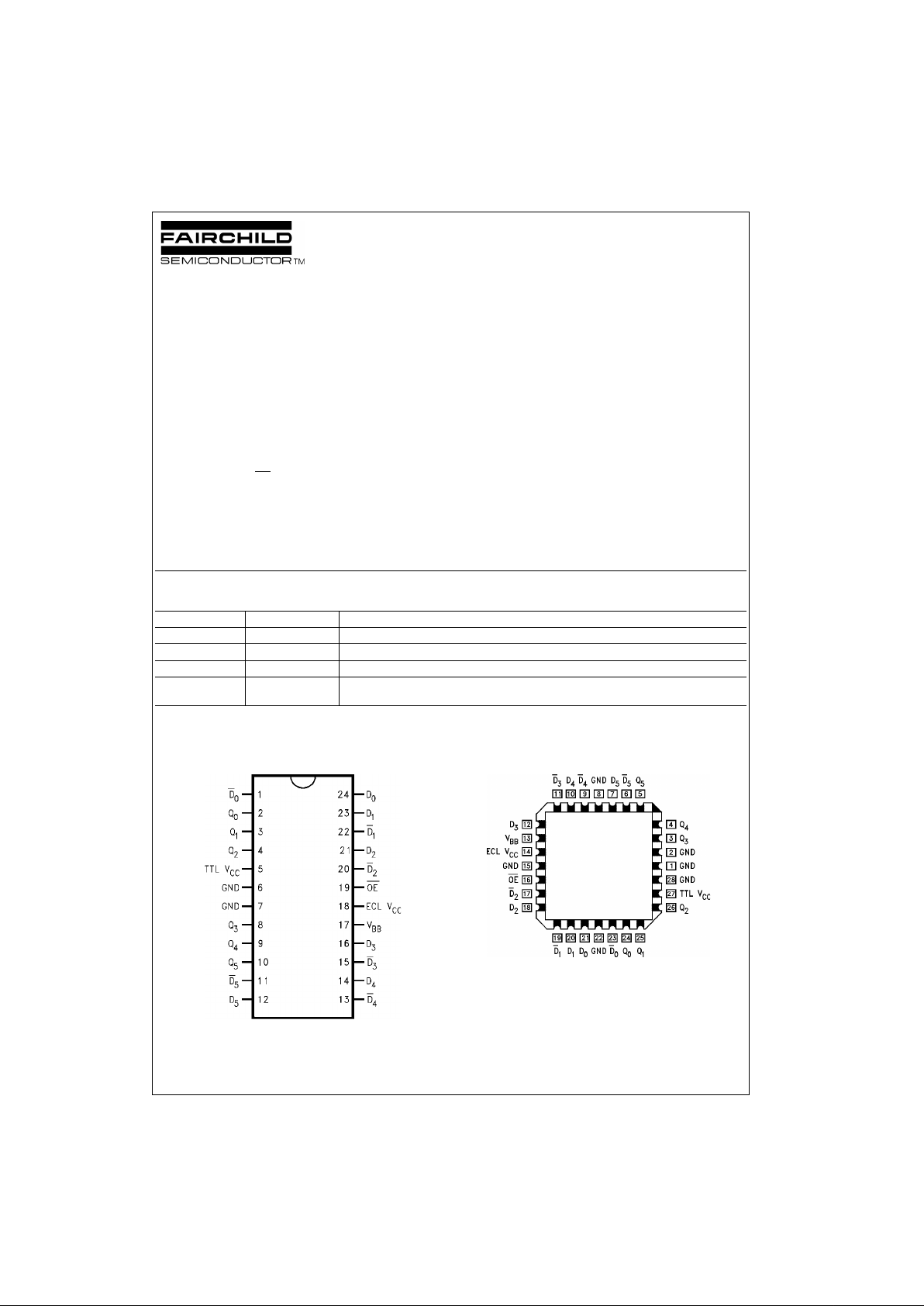
Connection Diagrams
24-Pin DIP/SOIC 28-Pin PLCC
FAST is a registered trademark of Fairc hild Semiconductor.
Order Number Package Number Package Description
100390SC M24B 24-Lead Small Outline Integrated Circuit (SOIC), JEDEC MS-013, 0.300 Wide
100390PC N24E 24-Lead Plastic Dual-In-Line Package (PDIP), JEDEC MS-010, 0.400 Wide
100390QC V28A 28-Lead Plastic Lead Chip Carrier (PLCC), JEDEC MO-047, 0.450 Square
100390QI V28A 28-Lead Plastic Lead Chip Carrier (PLCC), JEDEC MO-047, 0.450 Square
Industrial Temperature Range (
−40°C to +85°C)
Page 2
www.fairchildsemi.com 2
100390
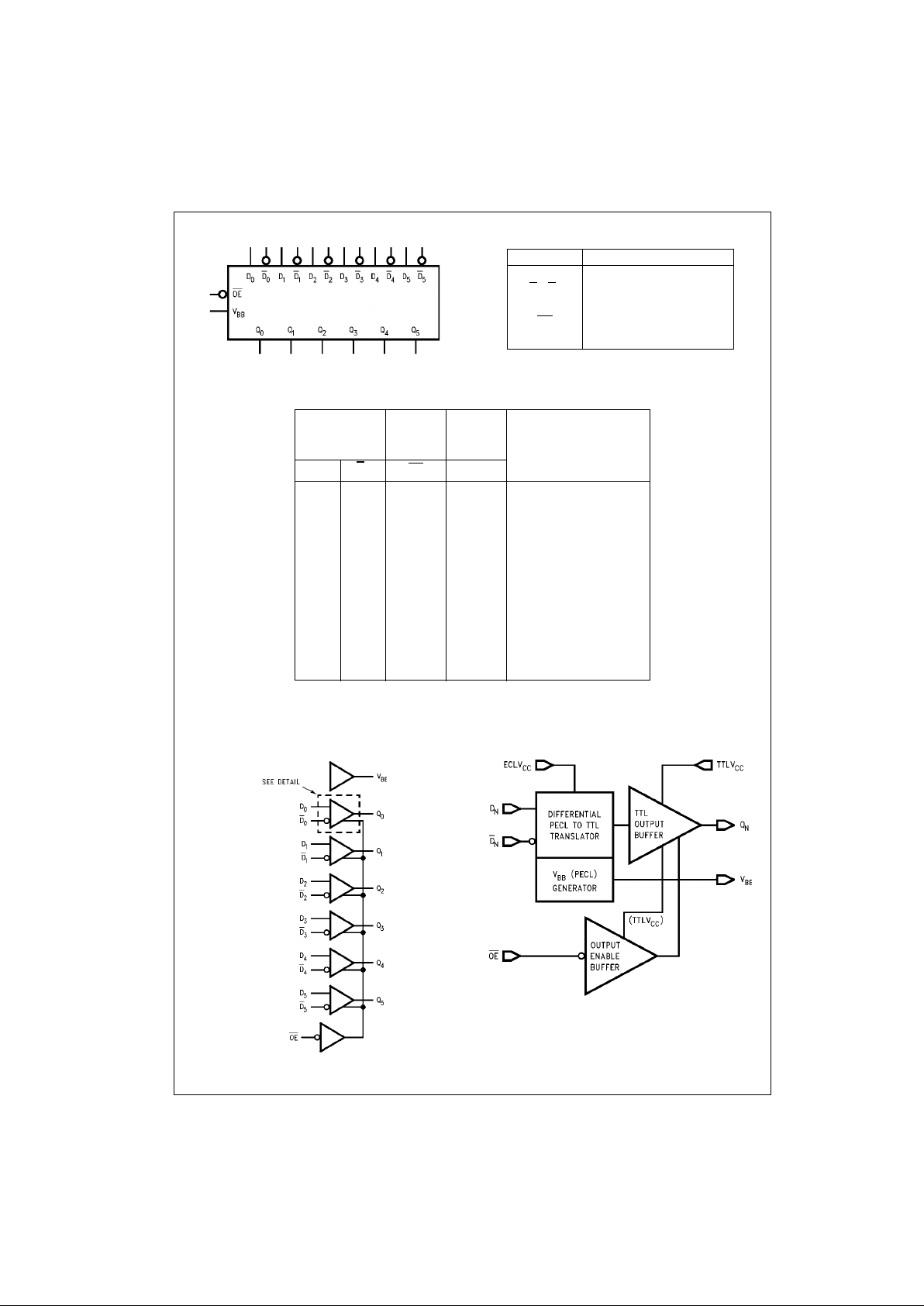
Logic Symbol Pin Descriptions
Truth Table
H = HIGH Voltage Level
L = LOW Voltage Level
Z = HIGH Impedance
U = Undefined
Logic Diagram Detail
Pin Names Description
D
0–D5
Data Inputs (PECL)
D
0–D5
Inverting Data Inputs (PECL)
Q
0–Q5
Data Outputs (TTL)
OE
Output Enable (TTL)
V
BB
Reference Voltage (PECL)
Data Control TTL
Comments
Inputs Input Outputs
(PECL) (TTL)
D
n
D
n
OE
Q
n
X X H Z Outputs Disable
L H L L Differential Operation
H L L H Differential Operation
L L L U Invalid Input States
H H L U Invalid Input States
OPEN OPEN L U Invalid Input States
LV
BB
L L Single Ended Operation
HV
BB
L H Single Ended Operation
V
BB
L L H Single Ended Operation
V
BB
H L L Single Ended Operation
V
BB
OPEN L H Single Ended Operation
OPEN V
BB
L L Single Ended Operation
Page 3
3 www.fairchildsemi.com
100390
Absolute Maximum Ratings(Note 1) Recommended Operating
Conditions
Note 1: The “Absolute Maximum Ratings” are those value s beyond which
the safety of the dev ice cannot b e guaranteed . The device sh ould not be
operated at these limit s. The parametric values defi ned in the Electrical
Characteristics tables are not guaranteed at the absolute maximum rating.
The “Recomm ended O peratin g Cond itions ” table will defin e the condition s
for actual device operation.
Note 2: Either voltage lim it or c urrent limit is sufficient to pro te c t in puts.
DC Electrical Characteristics
ECL V
CC
= +5.0V ±5%, TTL V
CC
= +5.0V ±5%, GND = 0V
Storage Temperature −65°C to +150°C
Maximum Junction Temperature
+150°C
V
CC
Pin Potential to Ground Pin −0.5V to +7.0V
TTL Input Voltage (Note 2)
−0.5V to +7.0V
TTL Input Current (Note 2)
−30 mA to +5.0 mA
V
BB
Output Current −5.0 mA to +1.0 mA
ECL Input Potential GND to ECL V
CC
+ 0.5V
V
CC
Differential
ECL V
CC
to TTL V
CC
−1.0V to +1.0V
Voltage Applied to Output
in High State (with V
CC
= 0V)
3-STATE Output
−0.5V to +5.5V
Current Applied to Output
in Low State (Max) Twice the Rated I
OL
(mA)
ESD Last Passing Voltage (Min) 2000V
Case Temperature 0
°C to +85°C
Supply Voltage
+4.75V to +5.25V
Symbol Parameter Min Max Units Conditions
V
IH
Input HIGH Voltage
Data ECL V
CC
− 1.165 ECL VCC − 0.870 V
Guaranteed HIGH Signal for ALL
Inputs (with One Input Tied to V
BB
)
OE 2.0 V Guaranteed HIGH Signal (TTL)
V
IL
Input LOW Voltage
Data ECL V
CC
− 1.830 ECL VCC − 1.475 V
Guaranteed LOW Signal for ALL
Inputs (with One Input Tied to VBB)
OE 0.8 V Guaranteed LOW Signal (TTL)
V
BB
Output Reference Voltage ECL VCC − 1.38 ECL VCC − 1.26 V IBB = 0.0 mA or −1.0 mA
V
OH
Output HIGH Voltage (TTL) 2.7 V IOH = −3 mA
V
OL
Output LOW Voltage (TTL) 0.5 V IOL = 24 mA
I
IH
Input HIGH Current
Data 50 µA
VIN = VIH(Max), D0–D5 = VBB,
D
0–D5
= VIL(Min)
OE 20 µAVIN = 2.7V (TTL)
I
IL
Input LOW Current OE −200 µAVIN = 0.5V (TTL)
I
BVI
Input Breakdown Current OE 10 µAVIN = 7.0V (TTL)
I
CBO
Input Leakage Current −10 µAVIN = GND, D0–D5 = V
BB
D0–D5 = VIL(Min)
I
OZH
3-STATE Current Output HIGH 50 µAV
OUT
= +2.7V
I
OZL
3-STATE Current Output LOW −50 µAV
OUT
= +0.5V
I
CC
ECL Supply Current 13 30 mA
I
CCZ
TTL Supply Current 10 20 mA 3-STATE
I
CCL
TTL Supply Current 8 17 mA Low State
I
CCH
TTL Supply Current HIGH 0.4 2.0 mA HIGH State
I
OS
Output Short-Circuit Current −150 −60 mA V
OUT
= 0.0V, VCC = +5.25
V
Diff
Differential Input Voltage 150 mV Required for Full Output Swing
V
CM
Common Mode Voltage ECL VCC − 2.0 ECL VCC − 0.5 V
V
CD
Clamp Diode Voltage −1.2 V IIN = −18 mA
Page 4

www.fairchildsemi.com 4
100390
DIP AC Electrical Characteristics
V
CC
= 5.0V ± 5%; T
C
= 0°C to +85°C
SOIC and PLCC Package AC Electrical Characteristics
V
CC
= 5.0V ± 5%; T
C
= 0°C to +85°C
Symbol Parameter
TC = 0°CT
C
= +25°CT
C
= +85°C
Units
Figure
Min Max Min Max Min Max Number
f
MAX
Maximum Clock Frequency 100 100 100 MHz
t
PLH
Propagation Delay
3.5 7.2 3.5 6.8 3.5 6.7 ns Figure 1
t
PHL
Data to Output
t
PZH
Output Enable Time 2.7 4.8 2.7 4.8 3.0 5.1
ns Figure 2
t
PZL
2.44.02.44.02.64.2
t
PHZ
Output Disable Time 2.9 5.8 2.9 5.4 2.7 5.1
ns Figure 2
t
PLZ
2.33.92.23.92.23.9
Symbol Parameter
TC = 0°CT
C
= +25°CT
C
= +85°C
Units
Figure
Min Max Min Max Min Max Number
f
MAX
Maximum Clock Frequency 100 100 100 MHz
t
PLH
Propagation Delay
3.5 7.0 3.5 6.6 3.5 6.5 ns Figure 1
t
PHL
Data to Output
t
PZH
Output Enable Time 2.7 4.6 2.7 4.6 3.0 4.9
ns Figure 2
t
PZL
2.43.82.43.82.64.0
t
PHZ
Output Disable Time 2.9 5.6 2.9 5.2 2.7 4.9
ns Figure 2
t
PLZ
2.33.72.23.72.23.7
Page 5

5 www.fairchildsemi.com
100390
Switching Waveforms
FIGURE 1. Data to Output Propagation Delay FIGURE 2. Enable/Disable Propagation Delay
Test Circuit
Notes:
GND = 0V, ECL V
CC
= +5V, TTL VCC = +5V
L1 and L2 = equal length 50Ω impedanc e lines
50Ω terminators are internal to S/H measure m ent unit
Decouplin g 0.1 µF from GND to ECL V
CC
and TTL V
CC
All unused outputs are loaded with 500Ω to GND
C
L
= Fixture and stray capacitance = 50 pF
Switch S1 is open for t
PLH
, t
PHL
, t
PHZ
and t
PZH
tests
Switch S1 is closed on ly fo r t
PLZ
and t
PZL
tests
FIGURE 3. AC Test Circuit
Page 6

www.fairchildsemi.com 6
100390
Application Notes
1. Device performance will be enhanced by the use of
dual V
CC
power planes as illustrated in the Application
Figures 4, 5. This will minimize the coupling of TTL
switching noise into the primary re ference to the ECL
circuitry and take full advantage of the 100390’s on
chip V
CC
partitioning.
2. The devic e’s partitioned V
CC
may be operated from two
5V, 5% tolerance, supplies provided that they are
ramped up/down together so that the max differential is
1V. This is to prevent overstress to internal ESD
diodes. If the ECL driver to the F390 is powered from a
separate supply, it must obey this sequence rule also.
3. Glitch-free power up, independent of Data input levels,
is achieved if TTL l ogic HIGH is held on the Output
Enable pin during ramping up/down of the V
CC
supply.
4. Undefined output states can occur for some invalid
combinations. See Truth Table. This should be avoided
to prevent possible oscillation or increased p ower consumption due to TTL outputs bi ased into a quasi state
with both pullup and pulldown stages partially on.
3-STATEing the outputs will counteract the effects of
invalid input states.
5. Pins 8, 15, and 22 on the 28-pin PLCC package are
tied to the chip’s substrate and are named GNDs.
These pins are electric ally comm on to the gro und pins
1, 2, and 28. For best thermal performance, tie the
GND pins to the circuit ground plane. They may be tied
to an electrically isolat ed thermal dissipation plane or
may float.
6. Figure 4 illustrates typical differential input operation.
7. Figure 5 illustrates typical single-ended input operation.
FIGURE 4.
FIGURE 5.
Page 7

7 www.fairchildsemi.com
100390
Physical Dimensions inches (millimeters) unless otherwise noted
24-Lead Small Outline Integrated Circuit (SOIC), JEDEC MS-013, 0.300 Wide
Package Number M24B
24-Lead Plastic Dual-In-Line Package (PDIP), JEDEC MS-010, 0.400 Wide
Package Number N24E
Page 8

www.fairchildsemi.com 8
100390 Low Power Single Supply Hex PECL-to-TTL Translator
Physical Dimensions inches (millimeters) unless otherwise noted (Continued)
28-Lead Plastic Lead Chip Carrier (PLCC), JEDEC MO-047, 0.450 Square
Package Number V28A
Fairchild does not assume any responsibility for use of any circuitr y described, no circuit patent licenses are implied and
Fairchild reserves the right at any time without notice to change said circuitry and specifications.
LIFE SUPPORT POLICY
FAIRCHILD’S PRODUCTS ARE NOT AUTHORIZED FOR USE AS CRITICAL COMPONENTS IN LIFE SUPPORT
DEVICES OR SYSTEMS WITHOUT THE EXPRESS WRITTEN APPROVAL OF THE PRESIDENT OF FAIRCHILD
SEMICONDUCTOR CORPORATION. As used herein:
1. Life support devices o r syste ms a re device s or syste ms
which, (a) are intended for surgical implant into the
body, or (b) support or sustain life, and (c) whose failure
to perform when properly used in accordance with
instructions for use provided in the labeling, can be reasonably expected to result in a significant inju ry to the
user.
2. A critical com ponent in any compon ent of a l ife supp ort
device or system whose failure t o perform can be reasonably expected to ca use the failure of the life supp ort
device or system, or to affect its safety or effectiveness.
www.fairchildsemi.com
 Loading...