

Datasheet 100364QIX, 100364QI, 100364QCX, 100364QC, 100364PC Datasheet (Fairchild Semiconductor)
Page 1
© 2000 Fairchild Semiconductor Corporation DS010265 www.fairchildsemi.com
February 1990
Revised August 2000
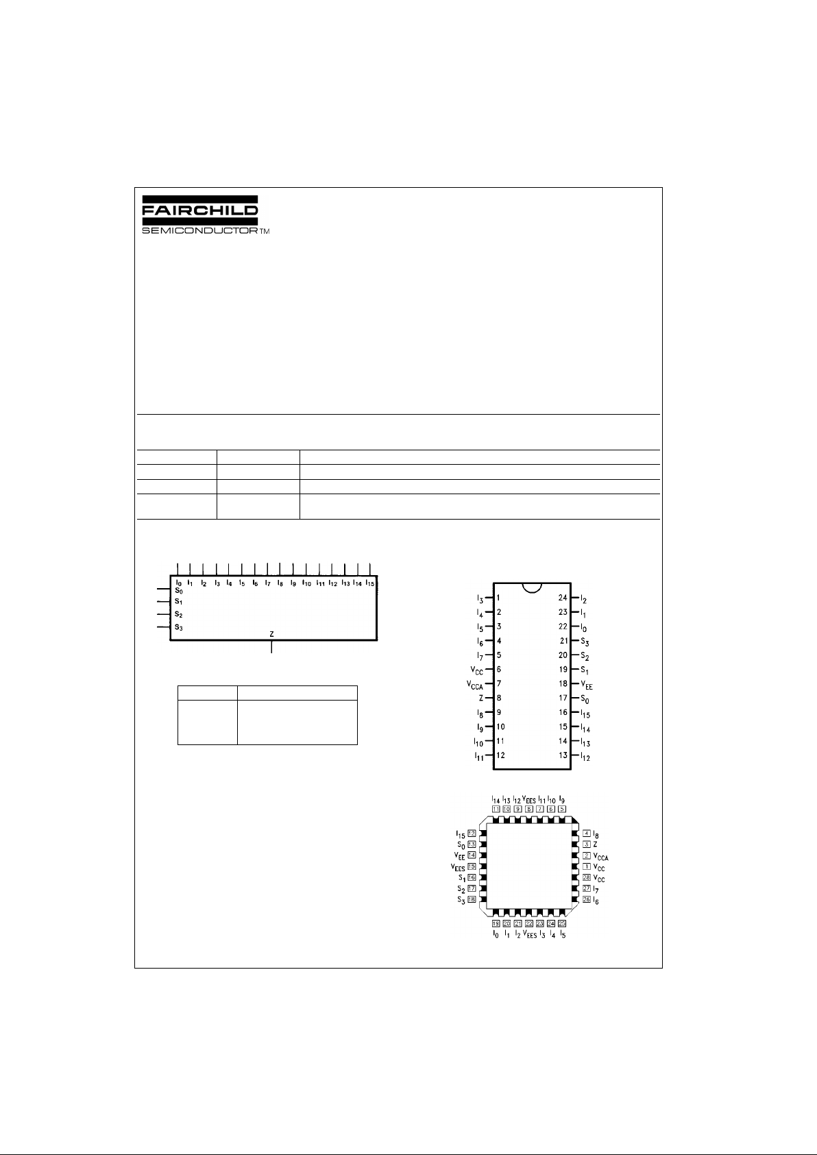
100364 Low Power 16-Input Multiplexer
100364
Low Power 16-Input Multiplexer
General Description
The 100364 is a 16-inpu t multiplexer. Data paths ar e controlled by four Select lines (S
0–S3
). Their decoding is
shown in the Truth Table. Output data polarity is the same
as the selected input data. All inputs have 50 k
Ω pull-down
resistors.
Features
■ 35% power reduction of the 100164
■ 2000V ESD protection
■ Pin/function compatible with 100164
■ Voltage compensated operating range
= −4.2V to −5.7V
■ Available to industrial grade temperature range
Ordering Code:
Devices also availab le in Tape and Reel. Specify by appending th e s uffix let t er “X” to the ordering code.
Logic Symbol
Pin Descriptions
Connection Diagrams
24-Pin DIP
28-Pin PLCC
Order Number Package Number Package Description
100364PC N24E 24-Lead Plastic Dual-In-Line Package (PDIP), JEDEC MS-010, 0.400 Wide
100364QC V28A 28-Lead Plastic Lead Chip Carrier (PLCC), JEDEC MO-047, 0.450 Square
100364QI V28A 28-Lead Plastic Lead Chip Carrier (PLCC), JEDEC MO-047, 0.450 Square
Industrial Temperature Range (
−40°C to +85°C)
Pin Names Description
I
0–I15
Data Inputs
S
0–S3
Select Inputs
Z Data Output
Page 2
www.fairchildsemi.com 2
100364
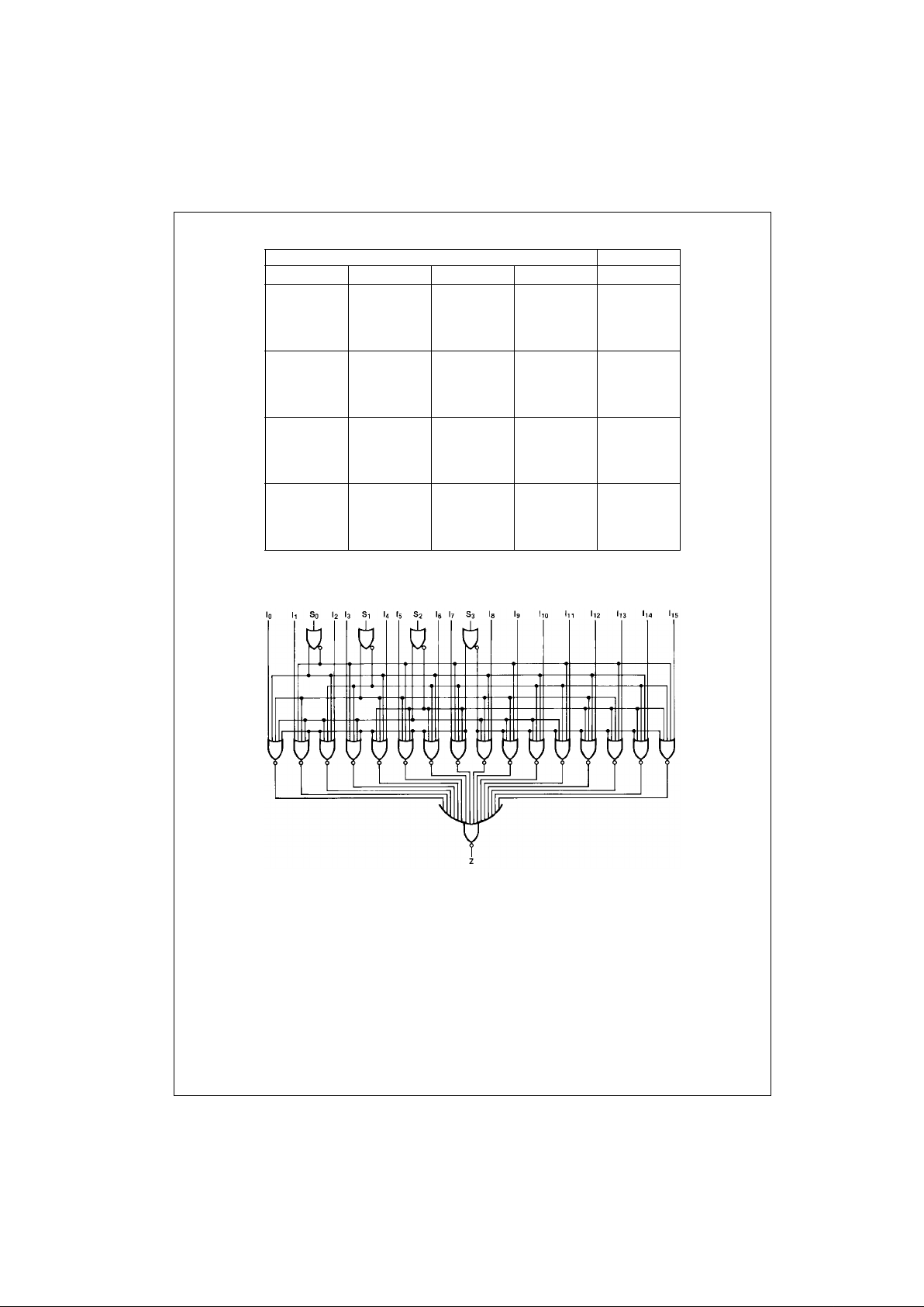
Truth Table
H = HIGH Voltage Level
L = LOW Voltage Level
Logic Diagram
Select Inputs Output
S
0
S
1
S
2
S
3
Z
LLLLI
0
HLLLI
1
LHLLI
2
HHL LI
3
LLHLI
4
HLHLI
5
LHHLI
6
HHHLI
7
LLLHI
8
HLLHI
9
LHLHI
10
HHLHI
11
LLHHI
12
HLHHI
13
LHHHI
14
HHHHI
15
Page 3
3 www.fairchildsemi.com
100364
Absolute Maximum Ratings(Note 1) Recommended Operating
Conditions
Note 1: The “Absolute Maximum Ratings” are those value s beyond which
the safety of the dev ice cannot b e guaranteed . The device sh ould not be
operated at these limit s. The parametric values defi ned in the Electrical
Characteristics tables are not guaranteed at the absolute maximum rating.
The “Recomm ended O peratin g Cond itions ” table will defin e the condition s
for actual device operation.
Note 2: ESD testing conforms to MIL-STD-883, Method 3015.
Commercial Version
DC Electrical Characteristics
(Note 3)
V
EE
= −4.2V to −5.7V, VCC = V
CCA
= GND, T
C
= 0°C to +85°C
Note 3: The specified limits represent the “worst case” value for the parameter. Since these values normally occur at the temperature extremes, additional
noise immunity and guardbanding can be achieved by decreasin g the al l owable syste m opera ti ng ran ge s. Cond it i ons fo r t estin g sho w n in the tabl es are chosen to guarantee operate under “worst case” conditions.
DIP AC Electrical Characteristics
V
EE
= −4.2V to −5.7V, VCC = V
CCA
= GND
Storage Temperature (T
STG
) −65°C to +150°C
Maximum Junction Temperature (T
J
) +150°C
Pin Potential to Ground Pin (V
EE
) −7.0V to +0.5V
Input Voltage (DC) V
EE
to +0.5V
Output Current
(DC Output HIGH)
−50 mA
ESD (Note 2)
≥ 2000V
Case Temperature (T
C
)
Commercial 0
°C to +85°C
Industrial
−40°C to +85°C
Supply Voltage (V
EE
) −5.7V to −4.2V
Symbol Parameter Min Typ Max Units Conditions
V
OH
Output HIGH Voltage −1025 −955 −870 mV VIN = VIH (Max) Loading with
V
OL
Output LOW Voltage −1830 −1705 −1620 mV or VIL (Min) 50Ω to −2.0V
V
OHC
Output HIGH Voltage −1035 mV VIN = VIH (Min) Loading with
V
OLC
Output LOW Voltage −1610 mV or VIL (Max) 50Ω to −2.0V
V
IH
Input HIGH Voltage −1165 −870 mV Guaranteed HIGH Signal
for All Inputs
V
IL
Input LOW Voltage −1830 −1475 mV Guaranteed LOW Signal
for All Inputs
I
IL
Input LOW Current 0.5 µAVIN = VIL (Min)
I
IH
Input HIGH Current 300 µAVIN = VIH (Max)
I
EE
Power Supply Current −89 −45 mA Inputs OPEN
Symbol Parameter
TC = 0°CT
C
= +25°CT
C
= +85°C
Units Conditions
Min Max Min Max Min Max
t
PLH
Propagation Delay
0.90 2.00 0.90 2.00 0.90 2.10 ns
t
PHL
I0–I15 to Output
t
PLH
Propagation Delay
1.40 2.80 1.40 2.80 1.50 2.90 ns
t
PHL
S0, S1 to Output Figures 1, 2
t
PLH
Propagation Delay
1.00 2.20 1.00 2.20 1.10 2.40 ns
t
PHL
S2, S3 to Output
t
TLH
Transition Time
0.35 1.20 0.35 1.20 0.35 1.20 ns
t
THL
20% to 80%, 80% to 20%
Page 4

www.fairchildsemi.com 4
100364
Commercial Version (Continued)
PLCC AC Electrical Characteristics
V
EE
= −4.2V to −5.7V, VCC = V
CCA
= GND
Industrial Version
PLCC DC Electrical Characteristics
(Note 4)
V
EE
= −4.2V to −5.7V, VCC = V
CCA
= GND, T
C
= −40°C to +85°C
Note 4: The specified limits represent the “worst case” value for the parameter. Since these values normally occur at the temperature extremes, additional
noise immunity and guardbanding can be achieved by decreasing the all owable syste m opera ti ng r ange s. Co ndi ti ons fo r t est ing shown in the ta ble s are chosen to guarantee operation under “worst case” conditions.
PLCC AC Electrical Characteristics
V
EE
= −4.2V to −5.7V, VCC = V
CCA
= GND
Symbol Parameter
T
C
= 0°CT
C
= +25°CT
C
= +85°C
Units Conditions
Min Max Min Max Min Max
t
PLH
Propagation Delay
0.90 1.80 0.90 1.80 0.90 1.90 ns
Figures 1, 2
t
PHL
I0–I15 to Output
t
PLH
Propagation Delay
1.40 2.60 1.40 2.60 1.50 2.70 ns
t
PHL
S0, S1 to Output
t
PLH
Propagation Delay
1.00 2.00 1.00 2.00 1.10 2.20 ns
t
PHL
S2, S3 to Output
t
TLH
Transition Time
0.35 1.10 0.35 1.10 0.35 1.10 ns
t
THL
20% to 80%, 80% to 20%
Symbol Parameter
TC = −40°CTC = 0°C to +85°C
Units Conditions
Min Max Min Max
V
OH
Output HIGH Voltage −1085 −870 −1025 −870 mV VIN = VIH (Max) Loading with
V
OL
Output LOW Voltage −1830 −1575 −1830 −1620 mV or VIL (Min) 50Ω to −2.0V
V
OHC
Output HIGH Voltage −1095 −1035 mV VIN = VIH (Min) Loading with
V
OLC
Output LOW Voltage −1565 −1610 mV or VIL (Max) 50Ω to −2.0V
V
IH
Input HIGH Voltage −1170 −870 −1165 −870 mV Guaranteed HIGH Signal for All Inputs
V
IL
Input LOW Voltage −1830 −1480 −1830 −1475 mV Guaranteed LOW Signal for All Inputs
I
IL
Input LOW Current 0.5 0.5 µA VIN = VIL (Min)
I
IH
Input HIGH Current 325 325 µA VIN = VIH (Max)
I
EE
Power Supply Current −89 −45 −89 −45 mA Inputs OPEN
Symbol Parameter
TC = −40°CT
C
= +25°CT
C
= +85°C
Units Conditions
Min Max Min Max Min Max
t
PLH
Propagation Delay
0.90 1.80 0.90 1.80 0.90 1.90 ns
Figures 1, 2
t
PHL
I0–I15 to Output
t
PLH
Propagation Delay
1.20 2.60 1.40 2.60 1.50 2.70 ns
t
PHL
S0, S1 to Output
t
PLH
Propagation Delay
0.80 2.10 1.00 2.00 1.10 2.20 ns
t
PHL
S2, S3 to Output
t
TLH
Transition Time
0.20 1.20 0.35 1.10 0.35 1.10 ns
t
THL
20% to 80%, 80% to 20%
Page 5

5 www.fairchildsemi.com
100364
Test Circuit
Note:
V
CC
, V
CCA
= +2V, VEE = −2.5V
L1 and L2 = Equal length 50Ω impedanc e lines
R
T
= 50Ω terminator internal to scope
Decouplin g 0.1 µF from GND to V
CC
and V
EE
All unused outputs are loaded with 50Ω to GND
C
L
= Fixture and stray capacitance ≤ 3 pF
FIGURE 1. AC Test Circuit
Switching Waveforms
FIGURE 2. Propagation Delay and Transition Times
Page 6

www.fairchildsemi.com 6
100364
Physical Dimensions inches (millimeters) unless otherwise noted
24-Lead Plastic Dual-In-Line Package (PDIP), JEDEC MS-010, 0.400 Wide
Package Number N24E
Page 7

7 www.fairchildsemi.com
100364 Low Power 16-Input Multiplexer
Physical Dimensions inches (millimeters) unless otherwise noted (Continued)
28-Lead Plastic Lead Chip Carrier (PLCC), JEDEC MO-047, 0.450 Square
Package Number V28A
Fairchild does not assume any responsibility for use of any circuitry described , no circuit patent licenses are implied and
Fairchild reserves the right at any time without notice to change said circuitry and specifications.
LIFE SUPPORT POLICY
FAIRCHILD’S PRODUCTS ARE NOT AUTHORIZED FOR USE AS CRITICAL COMPONENTS IN LIFE SUPPORT
DEVICES OR SYSTEMS WITHOUT THE EXPRESS WRITTEN APPROVAL OF THE PRESIDENT OF FAIRCHILD
SEMICONDUCTOR CORPORATION. As used herein:
1. Life support devices or systems are dev ic es or syste ms
which, (a) are intended for surgical implant into the
body, or (b) support or sustain life, and (c) whose failure
to perform when properly used in accordance with
instructions for use provide d in the labe l ing, can be re asonably expected to result in a significant injury to the
user.
2. A critical compo nent in any com ponen t of a life s upp ort
device or system whose failure to perform can be reasonably expected to cause the failure of the l ife support
device or system, or to affect its safety or effectiveness.
www.fairchildsemi.com
 Loading...