

Datasheet 100355QIX, 100355QI, 100355QCX, 100355QC, 100355PC Datasheet (Fairchild Semiconductor)
...Page 1
© 2000 Fairchild Semiconductor Corporation DS010147 www.fairchildsemi.com
July 1989
Revised August 2000
100355 Low Power Quad Multiplexer/Latch
100355
Low Power Quad Multiplexer/Latch
General Description
The 100355 contains four transparent latches, each of
which can accept an d store data from two sou rces. When
both Enable (E
n
) inputs are LOW, the data that appears at
an output is controlled by the Sel ect (S
n
) inputs, as shown
in the Operating Mod e table. In addition to routing data
from either D
0
or D1, the Select inputs can force the ou t-
puts LOW for the case wh er e th e latc h i s tr ansp ar ent (bo th
Enables are LOW) and can steer a HIGH signal from either
D
0
or D1 to an output. The Select inputs can be tied
together for applications requiring only that data be steered
from either D
0
or D1. A positive-going signal on either
Enable input latches the outputs. A HIGH signal on the
Master Reset (MR) input over rides all the ot her inputs and
forces the Q outputs LOW. All inputs have 50 k
Ω pull-down
resistors.
Features
■ Greater than 40% power reduction of the 100155
■ 2000V ESD protection
■ Pin/function compatible with 100155
■ Voltage compensated operating range
= −4.2V to −5.7V
■ Available to industrial grade temperature range
Ordering Code:
Devices also availab le in Tape and Reel. Specify by appending th e s uffix let t er “X” to the ordering code.
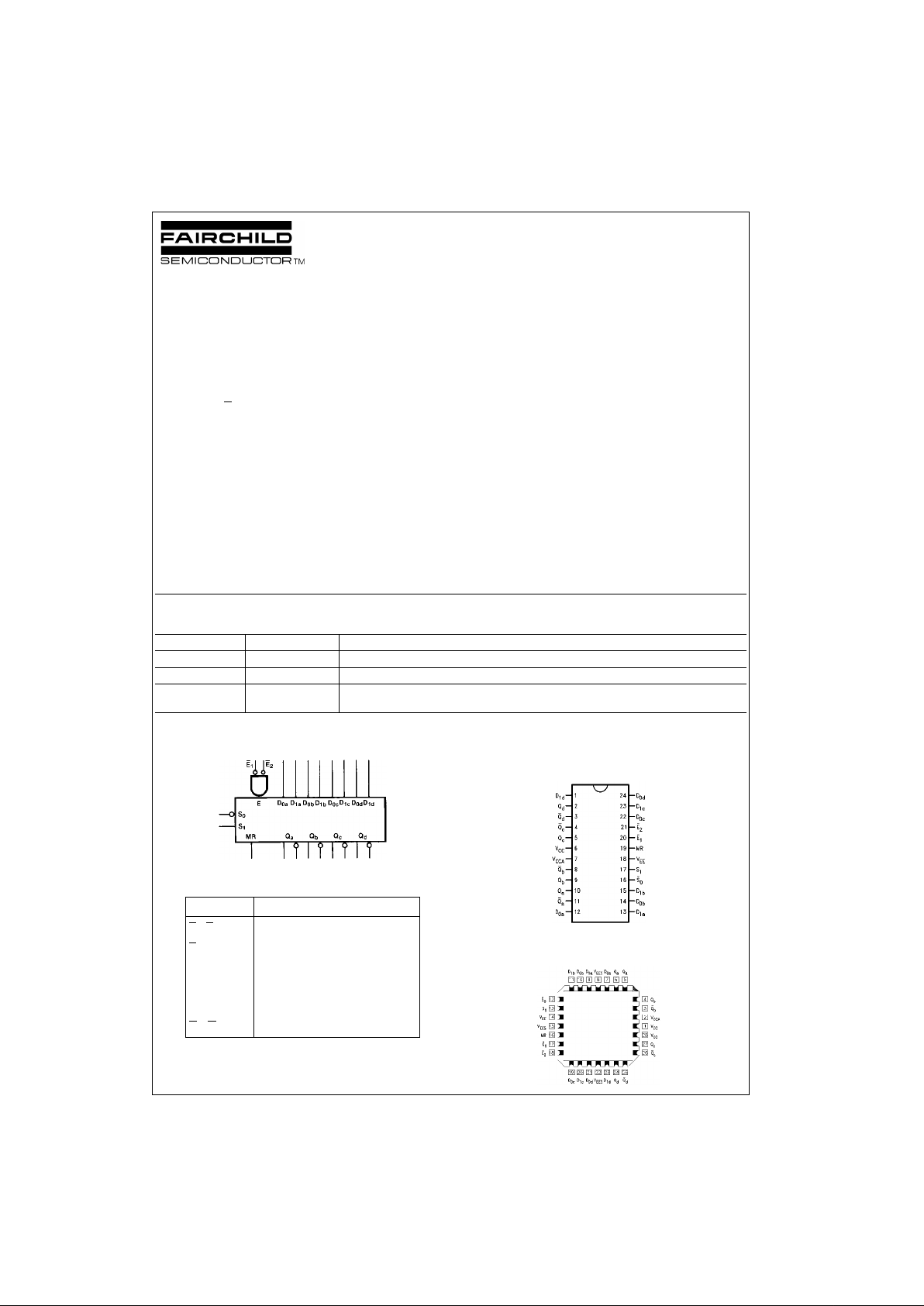
Logic Symbol
Pin Descriptions
Connection Diagrams
24-Pin DIP
28-Pin PLCC
Order Number Package Number Package Description
100355PC N24E 24-Lead Plastic Dual-In-Line Package (PDIP), JEDEC MS-010, 0.400 Wide
100355QC V28A 28-Lead Plastic Lead Chip Carrier (PLCC), JEDEC MO-047, 0.450 Square
100355QI V28A 28-Lead Plastic Lead Chip Carrier (PLCC), JEDEC MO-047, 0.450 Square
Industrial Temperature Range (
−40°C to +85°C)
Pin Names Description
E
1
, E
2
Enable Inputs (Active LOW)
S
0
, S
1
Select Inputs
MR Master Reset
D
na–Dnd
Data Inputs
Q
a–Qd
Data Outputs
Q
a–Qd
Complementary Data Outputs
Page 2
www.fairchildsemi.com 2
100355
Operating Mode Table
H = HIGH Voltage Level
L = LOW Voltage Level
X = Don’t Care
Note 1: Stores data present before E
went HIGH
Tr uth Table
Logic Diagram
Controls Outputs
E
1E2S1S0
Q
n
H X X X Latched (Note 1)
X H X X Latched (Note 1)
LLLL D
0x
LLHL D0x + D
1x
LLLH L
LLHH D
1x
Inputs Outputs
MR E
1E2S1S0D1xD0xQx
Q
x
HXXXXXX H L
LLLHHHX L H
LLLHHLX H L
LLLLLXH L H
LLLLLXL H L
LLLLHXX H L
LLLHLHX L H
LLLHLXH L H
LLLHLLL H L
L H X X X X X Latched (Note 1)
L X H X X X X Latched (Note 1)
Page 3
3 www.fairchildsemi.com
100355
Absolute Maximum Ratings(Note 2) Recommended Operating
Conditions
Note 2: The “Absolute Maximum Ratings” are those value s beyond which
the safety of the dev ice cannot b e guaranteed . The device sh ould not be
operated at these limit s. The parametric values defi ned in the Electrical
Characteristics tables are not guaranteed at the absolute maximum rating.
The “Recomm ended O peratin g Cond itions ” table will defin e the condition s
for actual device operation.
Note 3: ESD testing conforms to MIL-STD-883, Method 3015.
Commercial Version
DC Electrical Characteristics
(Note 4)
V
EE
= −4.2V to −5.7V, VCC = V
CCA
= GND, T
C
= 0°C to +85°C
Note 4: The specified limits represent the “worst case” value for the parameter. Since these values normally occur at the temperature extremes, additional
noise immunity and guard banding ca n be a chie ve d by decr easi ng the allowable system operating ranges. Conditions for testing shown in the tables are chosen to guarantee operation under “worst case” conditions.
Storage Temperature (T
STG
) −65°C to +150°C
Maximum Junction Temperature (T
J
) +150°C
V
EE
Pin Potential to Ground Pin −7.0V to +0.5V
Input Voltage (DC) V
EE
to +0.5V
Output Current (DC Output HIGH)
−50 mA
ESD (Note 3)
≥2000V
Case Temperature (T
C
)
Commercial 0
°C to +85°C
Industrial
−40°C to +85°C
Supply Voltage (V
EE
) −5.7V to −4.2V
Symbol Parameter Min Typ Max Units Conditions
V
OH
Output HIGH Voltage −1025 −955 −870 mV VIN = V
IH (Max)
Loading with
V
OL
Output LOW Voltage −1830 −1705 −1620 mV or V
IL (Min)
50Ω to −2.0V
V
OHC
Output HIGH Voltage −1035 mV VIN = V
IH (Min)
Loading with
V
OLC
Output LOW Voltage −1610 mV or V
IL (Max)
50Ω to −2.0V
V
IH
Input HIGH Voltage −1165 −870 mV Guaranteed HIGH Signal
for ALL Inputs
V
IL
Input LOW Voltage −1830 −1475 mV Guaranteed LOW Signal
for ALL Inputs
I
IL
Input LOW Current 0.50 µAVIN = V
IL (Min)
I
IH
Input HIGH Current
S
0
, S
1
220
E
1
, E
2
350 µAVIN = V
IH (Max)
Dna–D
nd
340
MR 430
I
EE
Power Supply Current −87 −40 mA Inputs Open
Page 4

www.fairchildsemi.com 4
100355
Commercial Version (Continued)
DIP AC Electrical Characteristics
V
EE
= −4.2V to −5.7V, VCC = V
CCA
= GND
Symbol Parameter
TC = 0°CT
C
= +25°CT
C
= +85°C
Units Conditions
Min Max Min Max Min Max
t
PLH
Propagation Delay
t
PHL
Dna–Dnd to Output 0.60 1.90 0.60 1.90 0.70 2.00 ns
(Transparent Mode)
t
PLH
Propagation Delay Figures 1, 2
t
PHL
S0, S1 to Output 1.00 2.60 1.00 2.60 1.20 2.70 ns
(Transparent Mode)
t
PLH
Propagation Delay
0.80 2.00 0.80 2.00 0.80 2.10 ns
t
PHL
E1, E2 to Output
t
PLH
Propagation Delay
0.80 2.30 0.80 2.30 0.80 2.30 ns Figures 1, 3
t
PHL
MR to Output
t
TLH
Transition Time
0.60 1.40 0.60 1.40 0.60 1.40 ns Figures 1, 2
t
THL
20% to 80%, 80% to 20%
t
S
Setup Time
Dna–D
nd
0.90 0.90 0.90 ns Figure 4
S
0
, S
1
1.70 1.70 1.70
MR (Release Time) 1.50 1.50 1.50 Figure 3
t
H
Hold Time
D
na–Dnd
0.40 0.40 0.40 ns Figure 4
S
0
, S
1
0.00 0.00 0.00
tPW (L) Pulse Width LOW E1, E
2
2.00 2.00 2.00 ns Figure 2
tPW (H) Pulse Width HIGH MR 2.00 2.00 2.00 ns Figure 3
Page 5

5 www.fairchildsemi.com
100355
Commercial Version (Continued)
PLCC AC Electrical Characteristics
V
EE
= −4.2V to −5.7V, VCC = V
CCA
= GND
Note 5: Output-to-Output Skew is defined as the absolute value of the difference between the actual propagation delay for any outputs within the same packaged device. The sp ecifica tions a pply to an y outp uts swit ching in the sam e direc tion eithe r HIGH -to-LOW (t
OSHL
), or LOW-to-HIGH (t
OSLH
), or in opposite
directions both HL and LH (t
OST
). Parameters t
OST
and tPS guaranteed by de s ign.
Symbol Parameter
TC = 0°CT
C
= +25°CT
C
= +85°C
Units Conditions
Min Max Min Max Min Max
t
PLH
Propagation Delay
t
PHL
Dna–Dnd to Output 0.60 1.70 0.60 1.70 0.70 1.80 ns
(Transparent Mode)
t
PLH
Propagation Delay Figures 1, 2
t
PHL
S0, S1 to Output 1.00 2.40 1.00 2.40 1.20 2.50 ns
(Transparent Mode)
t
PLH
Propagation Delay
0.80 1.80 0.80 1.80 0.80 1.90 ns
t
PHL
E1, E2 to Output
t
PLH
Propagation Delay
0.80 2.10 0.80 2.10 0.80 2.10 ns Figures 1, 3
t
PHL
MR to Output
t
TLH
Transition Time
0.60 1.30 0.60 1.30 0.60 1.30 ns Figures 1, 2
t
THL
20% to 80%, 80% to 20%
t
S
Setup Time
Dna–D
nd
0.80 0.80 0.80 ns Figure 4
S
0
, S
1
1.60 1.60 1.60
MR (Release Time) 1.40 1.40 1.40 Figure 3
t
H
Hold Time
D
na–Dnd
0.30 0.30 0.30 ns Figure 4
S
0
, S
1
−0.10 −0.10 −0.10
tPW (L) Pulse Width LOW E1, E
2
2.00 2.00 2.00 ns Figure 2
tPW (H) Pulse Width HIGH MR 2.00 2.00 2.00 ns Figure 3
t
OSHL
Maximum Skew Common Edge PLCC only
Output-to-Output Variation 330 330 330 ps (Note 5)
Data to Output Path
t
OSLH
Maximum Skew Common Edge PLCC only
Output-to-Output Variation 370 370 370 ps (Note 5)
Data to Output Path
t
OST
Maximum Skew Opposite Edge PLCC only
Output-to-Output Variation 370 370 370 ps (Note 5)
Data to Output Path
t
PS
Maximum Skew PLCC only
Pin (Signal) Transition Variation 270 270 270 ps (Note 5)
Data to Output Path
Page 6

www.fairchildsemi.com 6
100355
Industrial Version
PLCC DC Electrical Characteristics
(Note 6)
V
EE
= −4.2V to −5.7V, VCC = V
CCA
= GND, T
C
= −40°C to +85°C
Note 6: The specified limits represent the “worst case” value for the parameter. Since these values normally occur at the temperature extremes, additional
noise immunity and guard banding can be a ch ieve d by decr easi ng the allowable system operating rang es. Cond it i ons fo r testing shown in the tables are chosen to guarantee operation under “worst case” conditions.
PLCC AC Electrical Characteristics
V
EE
= −4.2V to −5.7V, VCC = V
CCA
= GND
Symbol Parameter
TC = −40°CTC = 0°C to +85°C
Units Conditions
Min Max Min Max
V
OH
Output HIGH Voltage −1085 −870 −1025 −870 mV VIN = V
IH (Max)
Loading with
V
OL
Output LOW Voltage −1830 −1575 −1830 −1620 mV or V
IL (Min)
50Ω to −2.0V
V
OHC
Output HIGH Voltage −1095 −1035 mV VIN = V
IH (Min)
Loading with
V
OLC
Output LOW Voltage −1565 −1610 mV or V
IL (Max)
50Ω to −2.0V
V
IH
Input HIGH Voltage −1170 −870 −1165 −870 mV Guaranteed HIGH Signal
for ALL Inputs
V
IL
Input LOW Voltage −1830 −1480 1830 1475 mV Guaranteed LOW Signal
for ALL Inputs
I
IL
Input LOW Current 0.50 0 .50 µAVIN = V
IL (Min)
I
IH
Input HIGH Current
S0, S
1
300 220
E1, E
2
350 350 µAVIN = V
IH (Max)
Dna–D
nd
340 340
MR 430 430
I
EE
Power Supply Current −87 −40 −87 −40 mA Inputs Open
Symbol Parameter
TC = −40°CT
C
= +25°CT
C
= +85°C
Units Conditions
Min Max Min Max Min Max
t
PLH
Propagation Delay
Figures 1, 2
t
PHL
Dna–Dnd to Output 0.60 1.70 0.60 1.70 0.70 1.80 ns
(Transparent Mode)
t
PLH
Propagation Delay
t
PHL
S0, S1 to Output 1.00 2.40 1.00 2.40 1.20 2.50 ns
(Transparent Mode)
t
PLH
Propagation Delay
0.80 1.80 0.80 1.80 0.80 1.90 ns
t
PHL
E1, E2 to Output
t
PLH
Propagation Delay
0.80 2.10 0.80 2.10 0.80 2.10 ns Figures 1, 3
t
PHL
MR to Output
t
TLH
Transition Time
0.40 1.90 0.60 1.30 0.60 1.30 ns Figures 1, 2
t
THL
20% to 80%, 80% to 20%
t
S
Setup Time
Dna–D
nd
0.90 0.80 0.80 ns Figure 4
S0, S
1
2.40 1.60 1.60
MR (Release Time) 1.50 1.40 1.40 Figure 3
t
H
Hold Time
Dna–D
nd
0.40 0.30 0.30 ns Figure 4
S0, S
1
0.00 −0.10 −0.10
tPW (L) Pulse Width LOW E1, E
2
2.00 2.00 2.00 ns Figure 2
tPW (H) Pulse Width HIGH MR 2.00 2.00 2.00 ns Figure 3
Page 7

7 www.fairchildsemi.com
100355
Test Circuit
Notes:
V
CC
, V
CCA
= +2V, VEE = −2.5V
L1 and L2 = equal length 50Ω impedanc e lines
R
T
= 50Ω terminator internal to scope
Decouplin g 0.1 µF from GND to V
CC
and V
EE
All unused outputs are loaded with 50Ω to GND
C
L
= Fixture and stray capacitance ≤ 3 pF
Pin numbers shown are for flat pak; for DIP see logic symbol
FIGURE 1. AC Test Circuit
Page 8

www.fairchildsemi.com 8
100355
Switching Waveforms
FIGURE 2. Enable Timing
FIGURE 3. Reset Timing
Notes:
t
S
is the minimum time bef ore the transition of the ena ble that information mu st be present at the data input.
t
H
is the minimum time after the transition of the ena ble that information must remain unchanged at th e data input.
FIGURE 4. Data Setup and Hold Times
Page 9

9 www.fairchildsemi.com
100355
Physical Dimensions inches (millimeters) unless otherwise noted
24-Lead Plastic Dual-In-Line Package (PDIP), JEDEC MS-010, 0.400 Wide
Package Number N24E
Page 10

www.fairchildsemi.com 10
100355 Low Power Quad Multiplexer/Latch
Physical Dimensions inches (millimeters) unless otherwise noted (Continued)
28-Lead Plastic Lead Chip Carrier (PLCC), JEDEC MO-047, 0.450 Square
Package Number V28A
Fairchild does not assume any responsibility for use of any circuitr y described, no circuit patent licenses are implied and
Fairchild reserves the right at any time without notice to change said circuitry and specifications.
LIFE SUPPORT POLICY
FAIRCHILD’S PRODUCTS ARE NOT AUTHORIZED FOR USE AS CRITICAL COMPONENTS IN LIFE SUPPORT
DEVICES OR SYSTEMS WITHOUT THE EXPRESS WRITTEN APPROVAL OF THE PRESIDENT OF FAIRCHILD
SEMICONDUCTOR CORPORATION. As used herein:
1. Life support devices or systems are devices or syste ms
which, (a) are intended for surgical implant into the
body, or (b) support or sustain life, and (c) whose failure
to perform when properly used in accordance with
instructions for use provided in the labeling, can be reasonably expected to result in a significant inju ry to the
user.
2. A critical component in any compon ent of a lif e supp ort
device or system whose failure t o perform can be reasonably expected to ca use the failure of the life supp ort
device or system, or to affect its safety or effectiveness.
www.fairchildsemi.com
 Loading...