

Datasheet 100353QIX, 100353QI, 100353QCX, 100353QC, 100353PC Datasheet (Fairchild Semiconductor)
Page 1
© 2000 Fairchild Semiconductor Corporation DS009882 www.fairchildsemi.com
July 1988
Revised August 2000
100353 Low Power 8-Bit Register
100353
Low Power 8-Bit Register
General Description
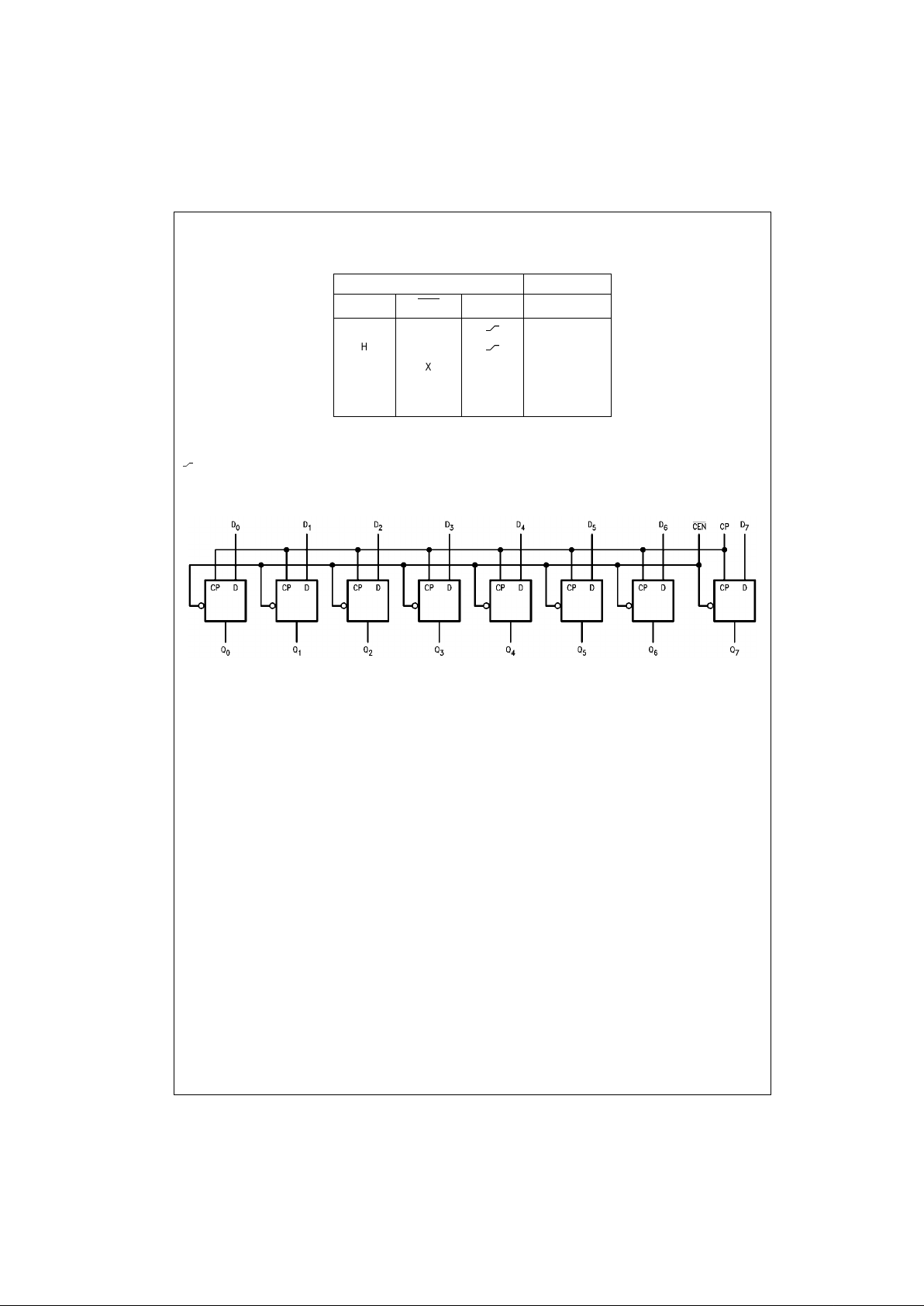
The 100353 contains eight D -type edge trigg ered, master/
slave flip-flops with individual inputs (D
n
), true outputs (Qn),
a clock input (CP), a nd a c omm on cl o ck e nab le p in ( C EN
).
Data enters the master when CP is LOW and transfers to
the slave when CP go es HIGH . When the CE N
input goes
HIGH it overrides all other inputs, disables the clock, and
the Q outputs maintain the last state.
The 100353 output drivers are designed to drive 50
Ω termi-
nation to
−2.0V. All inputs have 50 kΩ pull-down resistors.
Features
■ Low power operation
■ 2000V ESD protection
■ Voltage compensated operating range
= −4.2V to −5.7V
■ Available to industrial grade temperature range
Ordering Code:
Devices also availab le in Tape and Reel. Specify by appending th e s uffix let t er “X” to the ordering code.
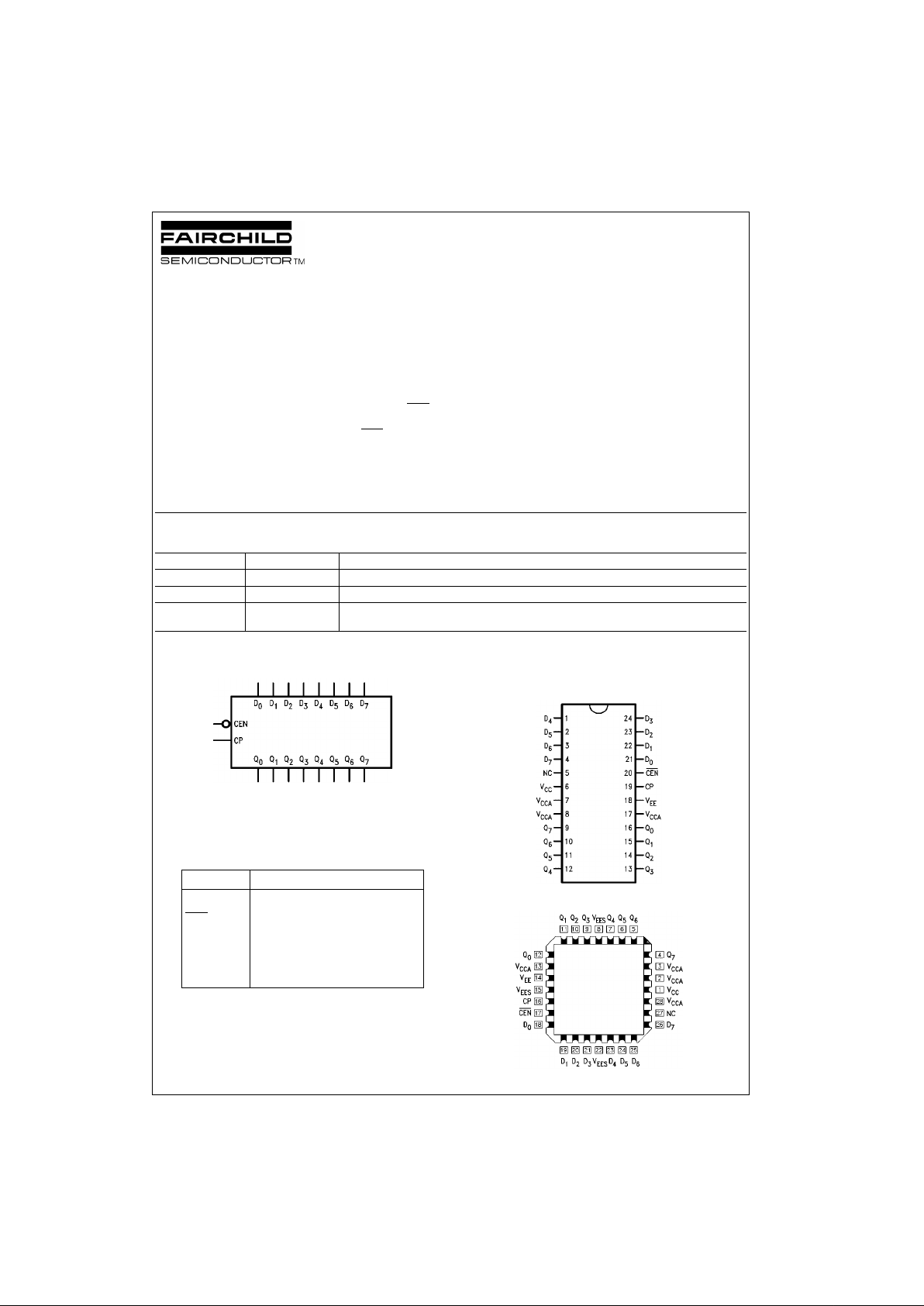
Logic Symbol
Pin Descriptions
Connection Diagrams
24-Pin DIP
28-Pin PLCC
Order Number Package Number Package Description
100353PC N24E 24-Lead Plastic Dual-In-Line Package (PDIP), JEDEC MS-010, 0.400 Wide
100353QC V28A 28-Lead Plastic Lead Chip Carrier (PLCC), JEDEC MO-047, 0.450 Square
100353QI V28A 28-Lead Plastic Lead Chip Carrier (PLCC), JEDEC MO-047, 0.450 Square
Industrial Temperature Range (
−40°C to +85°C)
Pin Names Description
D
0–D7
Data Inputs
CEN
Clock Enable Input
CP Clock Input (Active Rising Edge)
Q
0–Q7
Data Outputs
NC No Connect
Page 2
www.fairchildsemi.com 2
100353
Truth Table
H = HIGH Voltage Level
L = LOW Voltage Level
X = Don’t Care
NC = No Change
= LOW-to-HIGH Transition
Logic Diagram
Inputs Outputs
D
n
CEN CP Q
n
LL
L
HL
H
XXL NC
XXH NC
XHX NC
Page 3
3 www.fairchildsemi.com
100353
Absolute Maximum Ratings(Note 1) Recommended Operating
Conditions
Note 1: The “Absolute Maximum Ratings” are those value s beyond which
the safety of the dev ice cannot b e guaranteed . The device sh ould not be
operated at these limit s. The parametric values defi ned in the Electrical
Characteristics tables are not guaranteed at the absolute maximum rating.
The “Recomm ended O peratin g Cond itions ” table will defin e the condition s
for actual device operation.
Note 2: ESD testing conforms to MIL-STD-883, Method 3015.
Commercial Version
DC Electrical Characteristics
(Note 3)
V
EE
= −4.2V to −5.7V, VCC = V
CCA
= GND, T
C
= 0°C to +85°C
Note 3: The specified limits represent the “worst case” value for the parameter. Since these values normally occur at the temperature extremes, additional
noise immunity and guardbanding can be achieved by decreasin g the al l owable syste m opera ti ng ran ge s. Cond it i ons fo r t estin g sho w n in the tabl es are chosen to guarantee operation under “worst case” conditions.
DIP AC Electrical Characteristics
V
EE
= −4.2V to −5.7V, VCC = V
CCA
= GND
Note 4: The propagation delay s pec ified is for single output swit c hing. Delays may vary up to 300 ps with multiple outpu ts s witching.
Storage Temperature (T
STG
) −65°C to +150°C
Maximum Junction Temperature (T
J
) +150°C
V
EE
Pin Potential to Ground Pin −7.0V to +0.5V
Input Voltage (DC) V
EE
to + 0.5V
Output Current (DC Output HIGH)
−50 mA
ESD (Note 2)
≥2000V
Case Temperature (T
C
)
Commercial 0
°C to +85°C
Industrial
−40°C to +85°C
Supply Voltage (V
EE
) −5.7V to −4.2V
Symbol Parameter Min Typ Max Units Conditions
V
OH
Output HIGH Voltage −1025 −955 −870 mV VIN = VIH (Max) Loading with
V
OL
Output LOW Voltage −1830 −1705 −1620 mV or VIL (Min) 50Ω to −2.0V
V
OHC
Output HIGH Voltage −1035 mV VIN = VIH (Min) Loading with
V
OLC
Output LOW Voltage −1610 mV or VIL (Max) 50Ω to −2.0V
V
IH
Input HIGH Voltage −1165 −870 mV Guaranteed HIGH Signal for all Inputs
V
IL
Input LOW Voltage −1830 −1475 mV Guaranteed LOW Signal for all Inputs
I
IL
Input LOW Current 0.50 µAVIN = VIL (Min)
I
IH
Input HIGH Current 240 µAVIN = VIH (Max)
I
EE
Power Supply Current Inputs OPEN
−119 −61 mA V
EE
= −4.2V to −4.8V
−122 −61 V
EE
= −4.2V to −5.7V
Symbol Parameter
TC = 0°CT
C
= +25°CT
C
= +85°C
Units Conditions
Min Max Min Max Min Max
f
MAX
Toggle Frequency 425 425 425 MHz Figures 1, 2
t
PLH
Propagation Delay
1.40 3.00 1.40 3.00 1.50 3.10 ns
Figures 1, 2
t
PHL
CP to Output (Note 4)
t
TLH
Transition Time
0.45 2.00 0.45 2.00 0.45 2.00 ns Figures 1, 2
t
THL
20% to 80%, 80% to 20%
t
S
Setup Time
D
n
1.10 1.10 1.10
CEN (Disable Time) 0.40 0.40 0.40 ns Figures 1, 3
CEN (Release Time) 1.10 1.10 1.10
t
H
Hold Time
0.10 0.10 0.10 ns Figures 1, 4
D
n
tPW(H) Pulse Width HIGH
2.00 2.00 2.00 ns Figures 1, 2
CP
Page 4

www.fairchildsemi.com 4
100353
PLCC AC Electrical Characteristics
V
EE
= −4.2V to −5.7V, VCC = V
CCA
= GND
Note 5: The propagation dela y sp ec if ied is for single output swit c hing. Delays may vary up to 300 ps with multiple outpu ts s w it c hing.
Note 6: Output-to-Output Skew is defined as the absolute value of the difference between the actual propagation delay for any outputs within the same pack-
aged device. Th e specif ications apply to any out puts s witchin g in the sa me dire ction e ither HI GH-to-LO W ( t
OSHL
), or LOW-to-HIGH ( t
OSLH
), or in opposite
directions both HL and LH (t
OST
). Parameters t
OST
and tPS guaranteed by design.
Symbol Parameter
T
C
= 0°CT
C
= +25°CT
C
= +85°C
Units Conditions
Min Max Min Max Min Max
f
MAX
Toggle Frequency 425 425 425 MHz Figures 1, 2
t
PLH
Propagation Delay
1.40 2.80 1.40 2.80 1.50 2.90 ns
Figures 1, 2
t
PHL
CP to Output (Note 5)
t
TLH
Transition Time
0.45 1.90 0.45 1.90 0.45 1.90 ns Figures 1, 2
t
THL
20% to 80%, 80% to 20%
t
S
Setup Time
D
n
1.00 1.00 1.00
CEN
(Disable Time) 0.30 0.30 0.30 ns Figures 1, 3
CEN (Release Time) 1.00 1.00 1.00
t
H
Hold Time D
n
0 0 0 ns Figures 1, 4
t
PW
(H) Pulse Width HIGH CP 2.00 2.00 2.00 ns Figures 1, 2
t
OSHL
Maximum Skew Common Edge PLCC Only
Output-to-Output Variation 200 200 200 ps (Note 6)
Data to Output Path
t
OSLH
Maximum Skew Common Edge PLCC Only
Output-to-Output Variation 200 200 200 ps (Note 6)
Data to Output Path
t
OST
Maximum Skew Opposite Edge PLCC Only
Output-to-Output Variation 260 260 260 ps (Note 6)
Data to Output Path
t
PS
Maximum Skew PLCC Only
Pin (Signal) Transition Variation 280 280 280 ps (Note 6)
Data to Output Path
Page 5

5 www.fairchildsemi.com
100353
Industrial Version
PLCC DC Electrical Characteristics
V
EE
= −4.2V to −5.7V, VCC = V
CCA
= GND, TC = −40°C to +85°C (Note 7)
Note 7: The specified limits represent the “worst case” value for the parameter. Since these values normally occur at the temperature extremes, additional
noise immunity and guardbanding can be achieved by decreasin g the al l owable syste m opera ti ng ran ge s. Cond it i ons fo r t estin g sho w n in the tabl es are chosen to guarantee operation under “worst case” conditions.
PLCC AC Electrical Characteristics
V
EE
= −4.2V to −5.7V, VCC = V
CCA
= GND
Note 8: The propagation delay s pec ified is for single output swit c hing. Delays may vary up to 300 ps with multiple outpu ts s witching.
Symbol Parameter
T
C
= −40°CTC = 0°C to +85°C
Units Conditions
Min Max Min Max
V
OH
Output HIGH Voltage −1085 −870 −1025 −870 mV VIN = VIH (Max) Loading with
V
OL
Output LOW Voltage −1830 −1575 −1830 −1620 mV or VIL (Min) 50Ω to −2.0V
V
OHC
Output HIGH Voltage −1095 −1035 mV VIN = VIH (Min) Loading with
V
OLC
Output LOW Voltage −1565 −1610 mV or VIL (Max) 50Ω to −2.0V
V
IH
Input HIGH Voltage −1170 −870 −1165 −870 mV Guaranteed HIGH Signal for all Inputs
V
IL
Input LOW Voltage −1830 −1480 −1830 −1475 mV Guaranteed LOW Signal for all Inputs
I
IL
Input LOW Current 0.50 0.50 µAVIN = VIL (Min)
I
IH
Input HIGH Current 240 240 µAVIN = VIH (Max)
I
EE
Power Supply Current Inputs OPEN
−119 −61 −119 −61 mA V
EE
= −4.2V to −4.8V
−122 −61 −122 −61 VEE = −4.2V to −5.7V
Symbol Parameter
TC = −40°CT
C
= +25°CT
C
= +85°C
Units Conditions
Min Max Min Max Min Max
f
MAX
Toggle Frequency 425 425 425 MHz Figures 1, 2
t
PLH
Propagation Delay
1.40 2.80 1.40 2.80 1.50 2.90 ns
Figures 1, 2
t
PHL
CP to Output (Note 8)
t
TLH
Transition Time
0.40 2.50 0.45 1.90 0.45 1.90 ns Figures 1, 2
t
THL
20% to 80%, 80% to 20%
t
S
Setup Time
D
n
0.60 1.00 1.00
CEN (Disable Time) 0.90 0.30 0.30 ns Figures 1, 3
CEN
(Release Time) 1.40 1.00 1.00
t
H
Hold Time D
n
0.30 0 0 ns Figures 1, 4
tPW(H) Pulse Width HIGH CP 2.00 2.00 2.00 ns Figures 1, 2
Page 6

www.fairchildsemi.com 6
100353
Test Circuitry
Note:
• V
CC
, V
CCA
= +2V, VEE = −2.5V
• L1 and L2 = equal length 50Ω impedance lines
• R
T
= 50Ω terminator internal to scope
• Decoupling 0.1 µF from GND to V
CC
and V
EE
• All unused outputs are loaded with 50Ω to GND
• C
L
= Fixture and stray capacitance ≤ 3 pF
FIGURE 1. AC, Toggle Frequency Test Circuit
Switching Waveforms
FIGURE 2. Propagation Delay (Clock)
and Transition Times
FIGURE 3. Setup and Pulse Width Times
Note:
t
S
is the minimum time before the transition of the clock that information must be present at the data input.
t
H
is the minimum time after the transition of the clock that information must remain unchanged at the data input.
FIGURE 4. Data Setup and Hold Time
Page 7

7 www.fairchildsemi.com
100353
Physical Dimensions inches (millimeters) unless otherwise noted
24-Lead Plastic Dual-In-Line Package (PDIP), JEDEC MS-010, 0.400 Wide
Package Number N24E
Page 8

www.fairchildsemi.com 8
100353 Low Power 8-Bit Register
Physical Dimensions inches (millimeters) unless otherwise noted (Continued)
28-Lead Plastic Lead Chip Carrier (PLCC), JEDEC MO-047, 0.450 Square
Package Number V28A
Fairchild does not assume any responsibility for use of any circuitr y described, no circuit patent licenses are implied and
Fairchild reserves the right at any time without notice to change said circuitry and specifications.
LIFE SUPPORT POLICY
FAIRCHILD’S PRODUCTS ARE NOT AUTHORIZED FOR USE AS CRITICAL COMPONENTS IN LIFE SUPPORT
DEVICES OR SYSTEMS WITHOUT THE EXPRESS WRITTEN APPROVAL OF THE PRESIDENT OF FAIRCHILD
SEMICONDUCTOR CORPORATION. As used herein:
1. Life support de vices o r syste ms are device s or syste ms
which, (a) are intended for surgical implant into the
body, or (b) support or sustain life, and (c) whose failure
to perform when properly used in accordance with
instructions for use provided in the labeling, can be reasonably expected to result in a significant inju ry to the
user.
2. A critical compon ent in any com ponen t of a life su pport
device or system whose failure t o perform can be reasonably expected to ca use the failure of the life supp ort
device or system, or to affect its safety or effectiveness.
www.fairchildsemi.com
 Loading...