

Datasheet 100343QIX, 100343QI, 100343QCX, 100343QC, 100343PC Datasheet (Fairchild Semiconductor)
Page 1
© 2000 Fairchild Semiconductor Corporation DS010250 www.fairchildsemi.com
October 1989
Revised August 2000
100343 Low Power 8-Bit Latch
100343
Low Power 8-Bit Latch
General Description
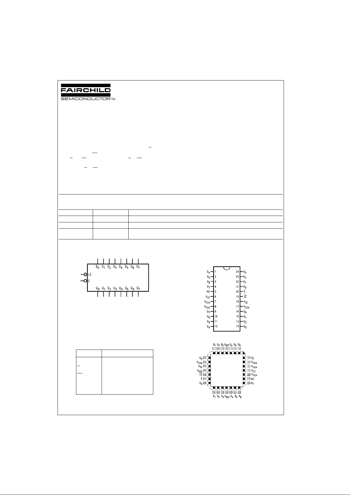
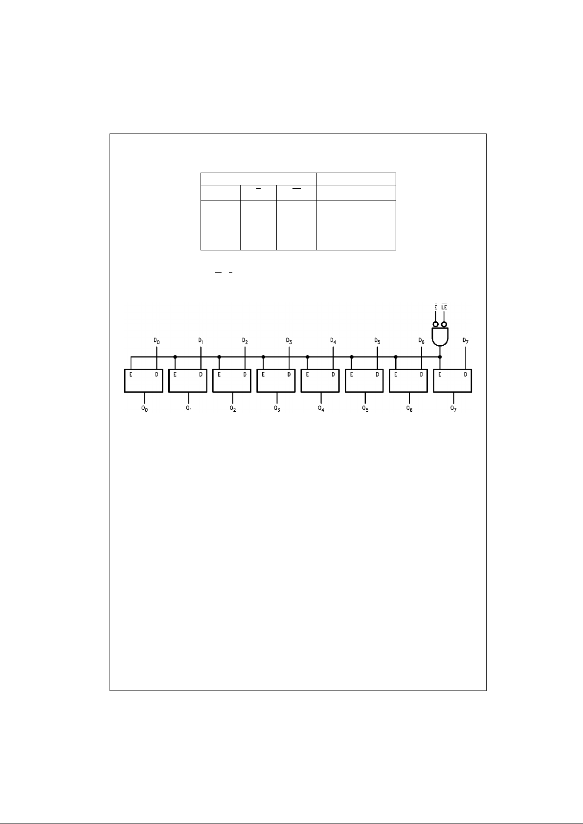
The 100343 contains eight D-type latches, individual
inputs, (D
n
), outputs (Qn), a common enab le p in ( E), and a
latch enable pin (LE
). A Q output follows its D input wh en
both E
and LE are LOW. When either E or LE (or both) are
HIGH, a latch stores th e last valid data present on its D
input prior to E
or LE going HIGH.
The 100343 outputs a re designed to drive a 50
Ω termina-
tion resistor to
−2.0V. All inputs have 50 kΩ pull-down
resistors.
Features
■ Low power operation
■ 2000V ESD protection
■ Voltage compensated operating range
= −4.2V to −5.7V
■ Available to industrial grade temperature range
Ordering Code:
Devices also availab le in Tape and Reel. Specify by appending th e s uffix let t er “X” to the ordering code.
Logic Symbol
Pin Descriptions
Connection Diagrams
24-Pin DIP
28-Pin PLCC
Order Number Package Number Package Description
100343PC N24E 24-Lead Plastic Dual-In-Line Package (PDIP), JEDEC MS-010, 0.400 Wide
100343QC V28A 28-Lead Plastic Lead Chip Carrier (PLCC), JEDEC MO-047, 0.450 Square
100343QI V28A 28-Lead Plastic Lead Chip Carrier (PLCC), JEDEC MO-047, 0.450 Square
Industrial Temperature Range (
−40°C to +85°C)
Pin Names Description
D
0–D7
Data Inputs
E
Enable Input
LE
Latch Enable Input
Q
0–Q7
Data Inputs
NC No Connect
Page 2
www.fairchildsemi.com 2
100343
Truth Table
H = HIGH Voltage Level
L = LOW Voltage Level
X = Don’t Care
Note 1: Retains data present before either LE
or E went HIGH
Logic Diagram
Inputs Outputs
D
n
E LE Q
n
LLL L
HLL H
X H X Latched (Note 1)
X X H Latched (Note 1)
Page 3
3 www.fairchildsemi.com
100343
Absolute Maximum Ratings(Note 2) Recommended Operating
Conditions
Note 2: The “Absolute Maximum Ratings” re those values beyond which
the safety of the dev ice cannot b e guaranteed . The device sh ould not be
operated at these limits. The parametric values def ined in the absolute
maximum rating. The “Recommended Operating Conditions” table will
define the conditio ns fo r ac t ual device operation.
Note 3: ESD testing conforms to MIL-STD-883, Method 3015.
Commercial Version
DC Electrical Characteristics
(Note 4)
V
EE
= −4.2V to −5.7V, VCC = V
CCA
= GND, T
C
= 0°C to +85°C
Note 4: The specified limits represent the “worst case” value for the parameter. Since these values normally occur at the temperature extremes, additional
noise immunity and guardbanding can be achieved by decreasin g the al l owable syste m opera ti ng ran ge s. Cond it i ons fo r t estin g sho w n in the tabl es are chosen to guarantee operation under “worst case” conditions.
AC Electrical Characteristics
V
EE
= −4.2V to −5.7V, VCC = V
CCA
= GND
Note 5: The propagation delay s pec ified is for single output swit c hing. Delays may vary up to 300 ps with multiple outpu ts s witching.
Storage Temperature (T
STG
) −65°C to +150°C
Maximum Junction Temperature (T
J
) +150°C
V
EE
Pin Potential to Ground Pin −7.0V to +0.5V
Input Voltage (DC) V
EE
to +0.5V
Output Current (DC Output HIGH)
−50 mA
ESD (Note 3)
≥2000V
Case Temperature (T
C
)
Commercial 0
°C to +85°C
Industrial
−40°C to +85°C
Supply Voltage (V
EE
) −5.7V to −4.2V
Symbol Parameter Min Typ Max Units Conditions
V
OH
Output HIGH Voltage −1025 −955 −870 mV VIN = VIH (Max) Loading with
V
OL
Output LOW Voltage −1830 −1705 −1620 mV or VIL (Min) 50Ω to −2.0V
V
OHC
Output HIGH Voltage −1035 mV VIN = VIH (Min) Loading with
V
OLC
Output LOW Voltage −1610 mV or VIL (Max) 50Ω to −2.0V
V
IH
Input HIGH Voltage −1165 −870 mV Guaranteed HIGH Signal for All Inputs
V
IL
Input LOW Voltage −1830 −1475 mV Guaranteed LOW Signal for All Inputs
I
IL
Input LOW Current 0.50 µAVIN = VIL (Min)
I
IH
Input HIGH Current 240 µAVIN = VIH (Max)
I
EE
Power Supply Current Inputs Open
−95 −55 mA V
EE
= −4.2V to −4.8V
−97 −55 V
EE
= −4.2V to −5.7V
Symbol Parameter
TC = 0°CT
C
= +25°CT
C
= +85°C
Units Conditions
Min Max Min Max Min Max
t
PLH
Propagation Delay
0.80 2.00 0.80 2.00 0.80 2.20 ns
Figures 1, 2, 3
t
PHL
Dn to Output (Note 5)
t
PLH
Propagation Delay
1.40 2.90 1.40 2.90 1.60 3.10 ns
Figures 1, 2, 3
t
PHL
LE, E to Output (Note 5)
t
TLH
Transition Time
0.45 2.00 0.45 2.00 0.45 2.00 ns Figures 1, 3
t
THL
20% to 80%, 80% to 20%
t
S
Setup Time D0–D71.0 1.0 1.1 ns Figures 1, 4
t
H
Hold Time D0–D70.1 0.1 0.1 ns Figures 1, 4
tPW(H) Pulse Width HIGH LE, E 2.00 2.00 2.00 ns Figures 1, 4
Page 4

www.fairchildsemi.com 4
100343
Commercial Version (Continued)
PLCC AC Electrical Characteristics
V
EE
= −4.2V to −5.7V, VCC = V
CCA
= GND
Note 6: The propagation dela y sp ec if ied is for single output swit c hing. Delays may vary up to 300 ps with multiple outpu ts s w it c hing.
Note 7: Output-to-Output Skew is defined as the absolute value of the difference between the actual propagation delay for any outputs within the same pack-
aged device. Th e specif ications apply to any out puts s witchin g in the sa me dire ction e ither HI GH-to-LO W ( t
OSHL
), or LOW-to-HIGH ( t
OSLH
), or in opposite
directions both HL and LH (t
OST
). Parameters t
OST
and tPS guaranteed by design.
Symbol Parameter
TC = 0°CT
C
= +25°CT
C
= +85°C
Units Conditions
MinMaxMinMaxMinMax
t
PLH
Propagation Delay
0.80 1.80 0.80 1.80 0.80 2.00 ns
Figures 1, 2, 3
t
PHL
Dn to Output (Note 6)
t
PLH
Propagation Delay
1.40 2.70 1.40 2.70 1.60 2.90 ns
Figures 1, 2, 3
t
PHL
LE, E to Output (Note 6)
t
TLH
Transition Time
0.45 1.90 0.45 1.90 0.45 1.90 ns Figures 1, 3
t
THL
20% to 80%, 80% to 20%
t
S
Setup Time D0–D70.90 0.90 1.00 ns Figures 1, 4
t
H
Hold Time D0–D
7
0.0 0.0 0.0 ns Figures 1, 4
tPW(H) Pulse Width HIGH LE, E 2.00 2.00 2.00 ns Figures 1, 4
t
OSHL
Maximum Skew Common Edge PLCC Only
Output-to-Output Variation 340 340 340 ps (Note 7)
Data to Output Path
t
OSLH
Maximum Skew Common Edge PLCC Only
Output-to-Output Variation 440 440 440 ps (Note 7)
Data to Output Path
t
OST
Maximum Skew Opposite Edge PLCC Only
Output-to-Output Variation 480 480 480 ps (Note 7)
Data to Output Path
t
PS
Maximum Skew PLCC Only
Pin (Signal) Transition Variation 300 300 300 ps (Note 7)
Data to Output Path
Page 5

5 www.fairchildsemi.com
100343
Industrial Version
PLCC DC Electrical Characteristics
(Note 8)
V
EE
= −4.2V to −5.7V, VCC = V
CCA
= GND, T
C
= −40°C to +85°C
Note 8: The specified limits represent the “worst case” value for the parameter. Since these values normally occur at the temperature extremes, additional
noise immunity and guardbanding can be achieved by decreasin g the al l owable syste m opera ti ng ran ge s. Cond it i ons fo r t estin g sho w n in the tabl es are chosen to guarantee operation under “worst case” conditions.
PLCC AC Electrical Characteristics
V
EE
= −4.2V to −5.7V, VCC = V
CCA
= GND
Note 9: The propagation delay s pec ified is for single output swit c hing. Delays may vary up to 300 ps with multiple outpu ts s witching.
Symbol Parameter
TC = −40°CTC = 0°C to +85°C
Units Conditions
Min Max Min Max
V
OH
Output HIGH Voltage −1085 −870 −1025 −870 mV VIN = V
IH (Max)
Loading with
V
OL
Output LOW Voltage −1830 −1575 −1830 −1620 mV or V
IL (Min)
50Ω to −2.0V
V
OHC
Output HIGH Voltage −1095 −1035 mV VIN = V
IH (Min)
Loading with
V
OLC
Output LOW Voltage −1565 −1610 mV or V
IL (Max)
50Ω to −2.0V
V
IH
Input HIGH Voltage −1170 −870 −1165 −870 mV Guaranteed HIGH Signal
for All Inputs
V
IL
Input LOW Voltage −1830 −1480 −1830 −1475 mV Guaranteed LOW Signal
for All Inputs
I
IL
Input LOW Current 0.50 0.50 µAVIN = VIL (Min)
I
IH
Input HIGH Current 240 240 µAVIN = VIH (Max)
I
EE
Power Supply Current Inputs Open
−95 −50 −95 −55 mA VEE = −4.2V to −4.8V
−97 −50 −97 −55 VEE = −4.2V to −5.7V
Symbol Parameter
T
C
= −40°CT
C
= +25°CT
C
= +85°C
Units Conditions
MinMaxMinMaxMinMax
t
PLH
Propagation Delay
0.80 1.80 0.80 1.80 0.80 2.00 ns
Figures 1, 2, 3
t
PHL
Dn to Output (Note 9)
t
PLH
Propagation Delay
1.40 2.70 1.40 2.70 1.60 2.90 ns
Figures 1, 2, 3
t
PHL
LE, E to Output (Note 9)
t
TLH
Transition Time
0.40 2.50 0.45 1.90 0.45 1.90 ns Figures 1, 3
t
THL
20% to 80%, 80% to 20%
t
s
Setup Time D0–D70.60 0.90 1.00 ns Figures 1, 4
t
H
Hold Time D0–D
7
0.8 0.0 0.0 ns Figures 1, 4
tpw(H) Pulse Width HIGH LE , E 2.40 2.00 2.00 ns Figures 1, 4
Page 6

www.fairchildsemi.com 6
100343
Test Circuitry
Note:
• V
CC
, V
CCA
= +2V, VEE = −2.5V
• L1 and L2 = equal length 50Ω impedance lines
• R
T
= 50Ω terminator internal to scope
• Decoupling 0.1 µF from GND to V
CC
and V
EE
• All unused outputs are loaded with 50Ω to GND
• C
L
= Fixture and stray capacitance ≤ 3 pF
FIGURE 1. AC Test Circuit
Switching Waveforms
FIGURE 2. Propagation Delays
FIGURE 3. Propagation and Transition Times
FIGURE 4. Setup, Hold and Pulse Width Times
Page 7

7 www.fairchildsemi.com
100343
Physical Dimensions inches (millimeters) unless otherwise noted
24-Lead Plastic Dual-In-Line Package (PDIP), JEDEC MS-010, 0.400 Wide
Package Number N24E
Page 8

www.fairchildsemi.com 8
100343 Low Power 8-Bit Latch
Physical Dimensions inches (millimeters) unless otherwise noted (Continued)
28-Lead Plastic Lead Chip Carrier (PLCC), JEDEC MO-047, 0.450 Square
Package Number V28A
Fairchild does not assume any responsibility for use of any circuitr y described, no circuit patent licenses are implied and
Fairchild reserves the right at any time without notice to change said circuitry and specifications.
LIFE SUPPORT POLICY
FAIRCHILD’S PRODUCTS ARE NOT AUTHORIZED FOR USE AS CRITICAL COMPONENTS IN LIFE SUPPORT
DEVICES OR SYSTEMS WITHOUT THE EXPRESS WRITTEN APPROVAL OF THE PRESIDENT OF FAIRCHILD
SEMICONDUCTOR CORPORATION. As used herein:
1. Life support devices or systems are devices or syste ms
which, (a) are intended for surgical implant into the
body, or (b) support or sustain life, and (c) whose failure
to perform when properly used in accordance with
instructions for use provided in the labeling, can be reasonably expected to result in a significant inju ry to the
user.
2. A critical component in any compon ent of a lif e supp ort
device or system whose failure t o perform can be reasonably expected to ca use the failure of the life supp ort
device or system, or to affect its safety or effectiveness.
www.fairchildsemi.com
 Loading...