

Page 1
100343
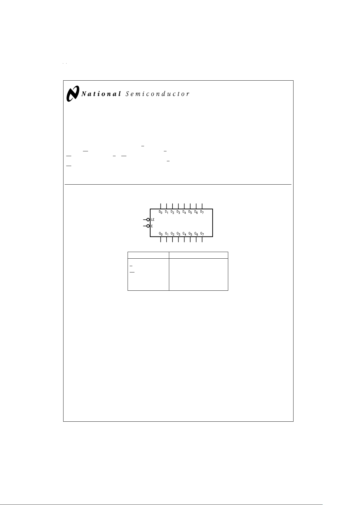
Low Power 8-Bit Latch
General Description
The 100343 contains eight D-type latches, individual inputs,
(D
n
), outputs (Qn), a commonenable pin (E), and a latch enable pin (LE). A Q output follows its D input when both E and
LE are LOW.When either E or LE (or both) are HIGH, a latch
stores the last valid data present on its D input prior to E or
LE going HIGH.
The 100343 outputs are designed to drive a 50Ω termination
resistor to −2.0V. All inputs have 50 kΩ pull-down resistors.
Features
n Low power operation
n 2000V ESD protection
n Voltage compensated operating range=−4.2V to −5.7V
n Available to MIL-STD-883
Logic Symbol
Pin Names Description
D
0–D7
Data Inputs
E
Enable Input
LE
Latch Enable Input
Q
0–Q7
Data Inputs
NC No Connect
DS100298-1
August 1998
100343 Low Power 8-Bit Latch
© 1998 National Semiconductor Corporation DS100298 www.national.com
Page 2
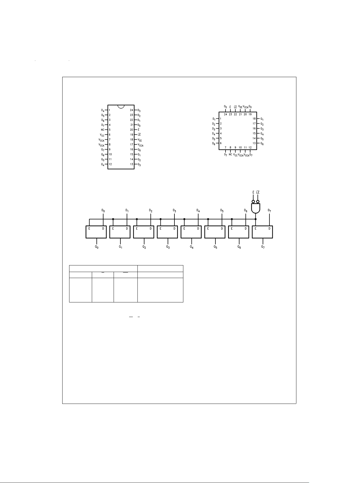
Connection Diagrams
Logic Diagram
Truth Table
Inputs Outputs
D
n
E LE Q
n
LLL L
HLL H
X H X Latched (Note 1)
X X H Latched (Note 1)
H=HIGH voltage level
L=LOW voltage level
X=Don’t care
Note 1: Retains data present before either LE or E went HIGH
24-Pin DIP
DS100298-2
24-Pin Quad Cerpak
DS100298-3
DS100298-5
www.national.com 2
Page 3
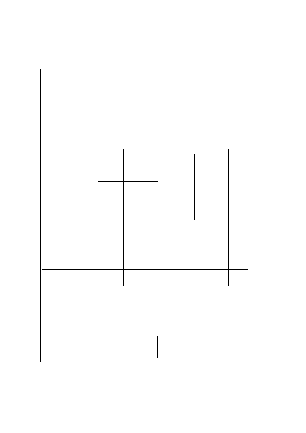
Absolute Maximum Ratings (Note 2)
If Military/Aerospace specified devices are required,
please contact the National Semiconductor Sales Office/
Distributors for availability and specifications.
Storage Temperature (T
STG
) −65˚C to +150˚C
Maximum Junction Temperature (T
J
)
Ceramic +175˚C
V
EE
Pin Potential to Ground Pin −7.0V to +0.5V
Input Voltage (DC) V
EE
to +0.5V
Output Current (DC Output HIGH) −50 mA
ESD (Note 3) ≥2000V
Recommended Operating
Conditions
Case Temperature (TC)
Military −55˚C to +125˚C
Supply Voltage (V
EE
) −5.7V to −4.2V
Note 2: Absolute maximum ratings are those values beyond which the device may be damaged or have its useful life impaired. Functional operation
under these conditions is not implied.
Note 3: ESD testing conforms to MIL-STD-883, Method 3015.
Military Version
DC Electrical Characteristics
V
EE
=
−4.2V to −5.7V, V
CC
=
V
CCA
=
GND, T
C
=
−55˚C to +125˚C
Symbol Parameter Min Max Units T
C
Conditions Notes
V
OH
Output HIGH Voltage −1025 −870 mV 0˚C to V
IN
=
V
IH
(Max)
or V
IL
(Min)
Loading with
50Ω to −2.0V
1, 2, 3
+125˚C
−1085 −870 mV −55˚C
V
OL
Output LOW Voltage −1830 −1620 mV 0˚C to
+125˚C
−1830 −1555 mV −55˚C
V
OHC
Output HIGH Voltage −1035 mV 0˚C to V
IN
=
V
IH
(Max)
or V
IL
(Min)
Loading with
50Ω to −2.0V
1, 2, 3
+125˚C
−1085 mV −55˚C
V
OLC
Output LOW Voltage −1610 mV 0˚C to
+125˚C
−1555 mV −55˚C
V
IH
Input HIGH Voltage −1165 −870 mV −55˚C to Guaranteed HIGH Signal for All Inputs 1, 2, 3, 4
+125˚C
V
IL
Input LOW Voltage −1830 −1475 mV −55˚C to Guaranteed LOW Signal for All Inputs 1, 2, 3, 4
+125˚C
I
IL
Input LOW Current 0.50 µA −55˚C to V
EE
=
−4.2V 1, 2, 3
+125˚C V
IN
=
V
IL
(Min)
I
IH
Input HIGH Current 240 µA 0˚C to V
EE
=
−5.7V
V
IN
=
V
IH
(Max)
1, 2, 3
+125˚C
340 µA −55˚C
I
EE
Power Supply Current −55˚C to Inputs Open
−100 −35 mA +125˚C V
EE
=
−4.2V to −4.8V 1, 2, 3
−105 −35 V
EE
=
−4.2V to −5.7V
Note 4: F100K 300 Series cold temperature testing is performed by temperature soaking (to guarantee junction temperature equals −55˚C), then testing immediately
without allowing for the junction temperature to stabilize due to heat dissipation after power-up. This provides “cold start” specs which can be consideredaworstcase
condition at cold temperatures.
Note 5: Screen tested 100%on each device at −55˚C, +25˚C, and +125˚C, Subgroups 1, 2, 3, 7, and 8.
Note 6: Sample tested (Method 5005, Table I) on each manufactured lot at −55˚C, +25˚C, and +125˚C, Subgroups A1, 2, 3, 7, and 8.
Note 7: Guaranteed by applying specified input condition and testing V
OH/VOL
.
Military Version
AC Electrical Characteristics
V
EE
=
−4.2V to −5.7V, V
CC
=
V
CCA
=
GND
Symbol Parameter T
C
=
−55˚C T
C
=
+25˚C T
C
=
+125˚C Units Conditions Notes
Min Max Min Max Min Max
t
PLH
Propagation Delay 0.50 2.70 0.50 2.30 0.50 2.80 ns
Figures 1, 2, 3
(Notes 8, 9,
10, 12)
t
PHL
Dnto Output
www.national.com3
Page 4

Military Version
AC Electrical Characteristics
(Continued)
V
EE
=
−4.2V to −5.7V, V
CC
=
V
CCA
=
GND
Symbol Parameter T
C
=
−55˚C T
C
=
+25˚C T
C
=
+125˚C Units Conditions Notes
Min Max Min Max Min Max
t
PLH
Propagation Delay 0.90 3.40 1.0 3.10 1.10 3.90 ns
Figures 1, 2, 3
(Notes 8, 9,
10, 12)
t
PHL
LE, E to Output
t
TLH
Transition Time 0.40 2.50 0.40 2.40 0.40 2.70 ns
Figures 1, 3
(Note 11)
t
THL
20%to 80%,80%to 20
%
t
s
Setup Time
D
0–D7
0.60 0.60 0.60 ns
Figures 1, 4
(Note 11)
t
h
Hold Time
D
0–D7
1.50 1.50 1.70 ns
Figures 1, 4
(Note 11)
t
pw
(H) Pulse Width HIGH
LE, E
2.40 2.40 2.40 ns
Figures 1, 4
(Note 11)
Note 8: F100K 300 Series cold temperature testing is performed by temperature soaking (to guarantee junction temperature equals −55˚C), then testing immediately
after power-up. This provides “cold start” specs which can be considered a worst case condition at cold temperatures.
Note 9: Screen tested 100%on each device at +25˚C temperature only, Subgroup A9.
Note 10: Sample tested (Method 5005, Table I) on each manufactured lot at +25˚C, SubgroupA9, and at +125˚C and −55˚C temperatures, Subgroups A10 and A11.
Note 11: Not tested at +25˚C, +125˚C, and −55˚C temperature (design characterization data).
Note 12: The propagation delay specified is for single output switching. Delays may vary up to 300 ps with multiple outputs switching.
Test Circuitry
Switching Waveforms
DS100298-6
Note 13: VCC,V
CCA
=
+2V, V
EE
=
−2.5V
Note 14: L1 and L2=equal length 50Ω impedance lines
R
T
=
50Ω terminator internal to scope
Decoupling 0.1 µF from GND to V
CC
and V
EE
All unused outputs are loaded with 50Ω to GND
C
L
=
Fixture and stray capacitance ≤ 3pF
FIGURE 1. AC Test Circuit
DS100298-7
FIGURE 2. Propagation Delays
www.national.com 4
Page 5

Switching Waveforms (Continued)
DS100298-8
FIGURE 3. Propagation and Transition Times
DS100298-9
FIGURE 4. Setup, Hold and Pulse Width Times
www.national.com5
Page 6

6
Page 7

Physical Dimensions inches (millimeters) unless otherwise noted
24-Pin Ceramic Dual-In-Line Package (D)
NS Package Number J24E
24-Lead Quad Cerpak (F)
NS Package Number W24B
www.national.com7
Page 8

LIFE SUPPORT POLICY
NATIONAL’S PRODUCTS ARE NOT AUTHORIZED FOR USE AS CRITICAL COMPONENTS IN LIFE SUPPORT DEVICES OR SYSTEMS WITHOUT THE EXPRESS WRITTEN APPROVAL OF THE PRESIDENT OF NATIONAL SEMICONDUCTOR CORPORATION. As used herein:
1. Life support devices or systems are devices or sys-
tems which, (a) are intended for surgical implant into
the body, or (b) support or sustain life, and whose failure to perform when properly used in accordance
with instructions for use provided in the labeling, can
be reasonably expected to result in a significant injury
to the user.
2. A critical component in any component of a life support
device or system whose failure to perform can be reasonably expected to cause the failure of the life support
device or system, or to affect its safety or effectiveness.
National Semiconductor
Corporation
Americas
Tel: 1-800-272-9959
Fax: 1-800-737-7018
Email: support@nsc.com
www.national.com
National Semiconductor
Europe
Fax: +49 (0) 1 80-530 85 86
Email: europe.support@nsc.com
Deutsch Tel: +49 (0) 1 80-530 85 85
English Tel: +49 (0) 1 80-532 78 32
Français Tel: +49 (0) 1 80-532 93 58
Italiano Tel: +49 (0) 1 80-534 16 80
National Semiconductor
Asia Pacific Customer
Response Group
Tel: 65-2544466
Fax: 65-2504466
Email: sea.support@nsc.com
National Semiconductor
Japan Ltd.
Tel: 81-3-5620-6175
Fax: 81-3-5620-6179
100343 Low Power 8-Bit Latch
National does not assume any responsibility for use of any circuitry described, no circuit patent licenses are implied and National reserves the right at any time without notice to change said circuitry and specifications.
 Loading...