

Datasheet 100341SCX, 100341QIX, 100341QI, 100341QCX, 100341QC Datasheet (Fairchild Semiconductor)
...Page 1
© 2000 Fairchild Semiconductor Corporation DS009880 www.fairchildsemi.com
July 1988
Revised August 2000
100341 Low Power 8-Bit Shift Register
100341
Low Power 8-Bit Shift Register
General Description
The 100341 contains eight edge-triggered, D-type flip-flops
with individual inputs (P
n
) and outputs (Qn) for parallel
operation, and with serial inputs (D
n
) and steering logic f or
bidirectional shifting. The flip-flops accept input data a
setup time before the positive -going transition of the clock
pulse and their outpu ts respond a pro pagation delay after
this rising clock edge.
The circuit operating mode is determined by the Select
inputs S
0
and S1, which are internally decoded to select
either “parallel entry”, “h old”, “shift left” or “shift right” as
described in the Truth Table. All inputs have 50 k
Ω pull-
down resistors.
Features
■ 35% power reduction of the 100141
■ 2000V ESD protection
■ Pin/function compatible with 100141
■ Voltage compensated operating range
= −4.2V to −5.7V
■ Available to industrial grade temperature range
Ordering Code:
Devices also availab le in Tape and Reel. Specify by appending th e s uffix let t er “X” to the ordering code.
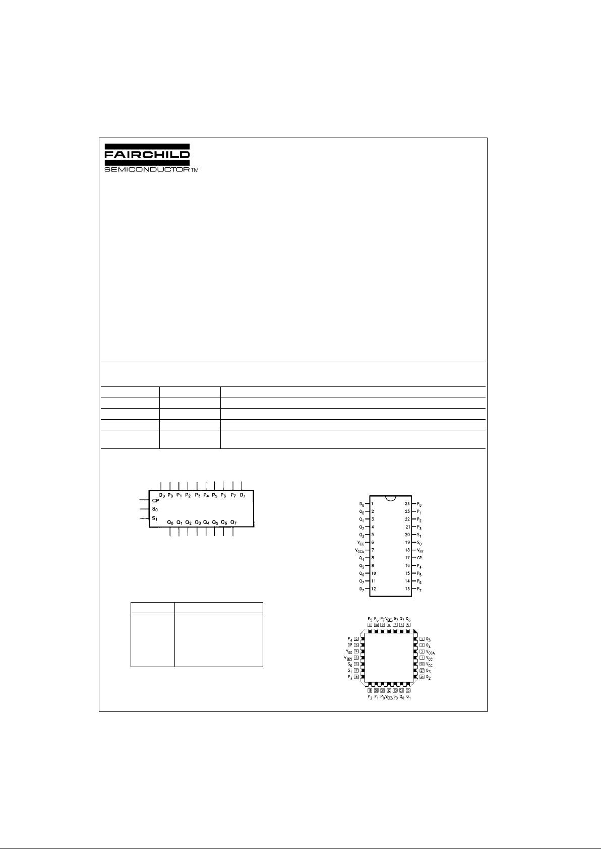
Logic Symbol
Pin Descriptions
Connection Diagrams
24-Pin DIP/SOIC
28-Pin PLCC
Order Number Package Number Package Description
10034SC M24B 24-Lead Small Outline Integrated Circuit (SOIC), JEDEC MS-013, 0.300 Wide
100341PC N24E 24-Lead Plastic Dual-In-Line Package (PDIP), JEDEC MS-010, 0.400 Wide
100341QI V28A 28-Lead Plastic Lead Chip Carrier (PLCC), JEDEC MO-047, 0.450 Square
100341QC V28A 28-Lead Plastic Lead Chip Carrier (PLCC), JEDEC MO-047, 0.450 Square
Industrial Temperature Range (
−40°C to +85°C)
Pin Names Description
CP Clock Input
S
0
, S
1
Select Inputs
D
0
, D
7
Serial Inputs
P
0–P7
Parallel Inputs
Q
0–Q7
Data Outputs
Page 2
www.fairchildsemi.com 2
100341
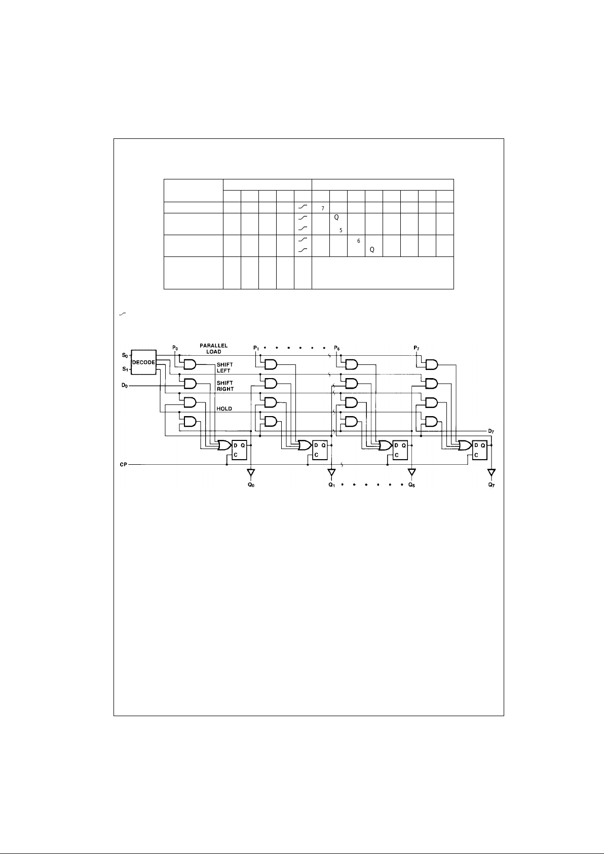
Truth Table
H = HIGH Voltage Level
L = LOW Voltage Level
X = Don’t Care
= LOW-to-HIGH Transition
Logic Diagram
Function
Inputs Outputs
D
7D0S1S0
CP Q7Q6Q5Q4Q3Q2Q1Q
0
Load Register X X L L
P7P6P5P4P3P2P1P
0
Shift Left X L L H
Q6Q5Q4Q3Q2Q1Q0L
Shift Left X H L H
Q6Q5Q4Q3Q2Q1Q0H
Shift Right L X H L
LQ7Q6Q5Q4Q3Q2Q
1
Shift Right H X H L
HQ7Q6Q5Q4Q3Q2Q
1
Hold X X H H X
Hold XXXXH No Change
Hold XXXXL
Page 3
3 www.fairchildsemi.com
100341
Absolute Maximum Ratings(Note 1) Recommended Operating
Conditions
Note 1: The “Absolute Maximum Ratings” are those value s beyond which
the safety of the dev ice cannot b e guaranteed . The device sh ould not be
operated at these limit s. The parametric values defi ned in the Electrical
Characteristics tables are not guaranteed at the absolute maximum rating.
The “Recomm ended O peratin g Cond itions ” table will defin e the condition s
for actual device operation.
Note 2: ESD testing conforms to MIL-STD-883, Method 3015.
Commercial Version
DC Electrical Characteristics
(Note 3)
V
EE
= −4.2V to −5.7V, VCC = V
CCA
= GND, T
C
= 0°C to +85°C
Note 3: The specified limits represent the “worst case” value for the parameter. Since these values normally occur at the temperature extremes, additional
noise immunity and guardbanding can be achieved by decreasin g the al l owable syste m opera ti ng ran ge s. Cond it i ons fo r t estin g sho w n in the tabl es are chosen to guarantee operation under “worst case” conditions.
DIP AC Electrical Characteristics
V
EE
= −4.2V to −5.7V, VCC = V
CCA
= GND
Note 4: The propagation delay specified is for the switching of a single output. Delays may vary up to 0.40 ns if multiple outputs are switching simultaneously.
Storage Temperature (T
STG
) −65°C to +150°C
Maximum Junction Temperature (T
J
) +150°C
V
EE
Pin Potential to Ground Pin −7.0V to +0.5V
Input Voltage (DC) V
EE
to +0.5V
Output Current (DC Output HIGH)
−50 mA
ESD (Note 2)
≥2000V
Case Temperature (T
C
)
Commercial 0
°C to +85°C
Industrial
−40°C to +85°C
Supply Voltage (V
EE
) −5.7V to −4.2V
Symbol Parameter Min Typ Max Units Conditions
V
OH
Output HIGH Voltage −1025 −955 −870 mV VIN = VIH (Max) Loading with
V
OL
Output LOW Voltage −1830 −1705 −1620 mV or VIL (Min) 50Ω to −2.0V
V
OHC
Output HIGH Voltage −1035 mV VIN = VIH (Min) Loading with
V
OLC
Output LOW Voltage −1610 mV or VIL (Max) 50Ω to −2.0V
V
IH
Input HIGH Voltage −1165 −870 mV Guaranteed HIGH Signal
for all Inputs
V
IL
Input LOW Voltage −1830 −1475 mV Guaranteed LOW Signal
for all Inputs
I
IL
Input LOW Current 0.50 µAVIN = VIL (Min)
I
IH
Input HIGH Current 240 µAVIN = VIH (Max)
I
EE
Power Supply Current Inputs OPEN
−157 −75 mA VEE = −4.2V to −4.8V
−167 −75 mA V
EE
= −4.2V to −5.7V
Symbol Parameter
TC = 0°CT
C
= +25°CT
C
= +85°C
Units Conditions
Min Max Min Max Min Max
f
MAX
Max Clock Frequency 400 400 400 MHz Figures 2, 3
t
PLH
Propagation Delay
0.90 1.90 1.00 2.00 1.00 2.10 ns
Figures 1, 3
t
PHL
CP to Output (Note 4)
t
TLH
Transition Time
0.35 1.30 0.35 1.30 0.35 1.30 ns Figures 1, 3
t
THL
20% to 80%, 80% to 20%
t
S
Setup Time Dn, P
n
0.65 0.65 0.65 ns
Figure 4
S
n
1.60 1.60 1.60
t
H
Hold Dn, P
n
0.80 0.80 0.80 ns
S
n
0.60 0.60 0.60
tPW(H) Pulse Width HIGH CP 2.00 2.00 2.00 ns Figure 3
Page 4

www.fairchildsemi.com 4
100341
Commercial Version (Continued)
SOIC and PLCC AC Electrical Characteristics
V
EE
= −4.2V to −5.7V, VCC = V
CCA
= GND
Note 5: The propagation delay specified is for the switching of a single output. Delays may vary up to 0.40 ns if multiple outputs are switching simultaneously.
Note 6: Output-to-Output Skew is defined as the absolute value of the difference between the actual propagation delay for any outputs within the same pack-
aged device. Th e specif ications apply to any out puts s witchin g in the sa me dire ction e ither HI GH-to-LO W ( t
OSHL
), or LOW-to-HIGH ( t
OSLH
), or in opposite
directions both HL and LH (t
OST
). Parameters t
OST
and tPS guaranteed by design
Symbol Parameter
TC = 0°CT
C
= +25°CT
C
= +85°C
Units Conditions
Min Max Min Max Min Max
f
MAX
Maximum Clock Frequency 425 425 425 MHz Figures 2, 3
t
PLH
Propagation Delay
0.90 1.70 1.00 1.80 1.00 1.90 ns
Figures 1, 3
t
PHL
CP to Output (Note 5)
t
TLH
Transition Time
0.35 1.20 0.35 1.20 0.35 1.20 ns Figures 1, 3
t
THL
20% to 80%, 80% to 20%
t
S
Setup Time Dn, Pn0.55 0.55 0.55
ns
S
n
1.50 1.50 1.50
Figure 4
t
H
Hold Time Dn, Pn0.70 0.70 0.70
ns
S
n
0.50 0.50 0.50
tPW(H) Pulse Width HIGH CP 2.00 2.00 2.00 ns Figure 3
t
OSHL
Maximum Skew Common Edge PLCC Only
Output-to-Output Variation 200 200 200 ps (Note 6)
Clock to Output Path
t
OSLH
Maximum Skew Common Edge PLCC Only
Output-to-Output Variation 200 200 200 ps (Note 6)
Clock to Output Path
t
OST
Maximum Skew Opposite Edge PLCC Only
Output-to-Output Variation 250 250 250 ps (Note 6)
Clock to Output Path
t
ps
Maximum Skew PLCC Only
Pin (Signal) Transition Variation 250 250 250 ps (Note 6)
Clock to Output Path
Page 5

5 www.fairchildsemi.com
100341
Industrial Version
PLCC DC Electrical Characteristics
(Note 7)
V
EE
= −4.2V to −5.7V, VCC = V
CCA
= GND, T
C
= −40°C to +85°C
Note 7: The specified limits represent the “worst case” value for the parameter. Since these values normally occur at the temperature extremes, additional
noise immunity and guardbanding can be achieved by decreasin g the al l owable syste m opera ti ng ran ge s. Cond it i ons fo r t estin g sho w n in the tabl es are chosen to guarantee operation under “worst case” conditions.
PLCC AC Electrical Characteristics
V
EE
= −4.2V to −5.7V, VCC = V
CCA
= GND
Note 8: The propagation delay specified is for the switching of a single output. Delays may vary up to 0.40 ns if multiple outputs are switching simultaneously.
Symbol Parameter
T
C
= −40°CTC = 0°C to +85°C
Units Conditions
Min Max Min Max
V
OH
Output HIGH Voltage −1085 −870 −1025 −870 mV VIN = VIH(Max) Loading with
V
OL
Output LOW Voltage −1830 −1575 −1830 −1620 mV or VIL (Min) 50Ω to −2.0V
V
OHC
Output HIGH Voltage −1095 −1035 mV VIN = VIH (Min) Loading with
V
OLC
Output LOW Voltage −1565 −1610 mV or VIL (Max) 50Ω to −2.0V
V
IH
Input HIGH Voltage −1170 −870 −1165 −870 mV Guaranteed HIGH Signal
for all Inputs
V
IL
Input LOW Voltage −1830 −1480 −1830 −1475 mV Guaran teed LOW Signal
for all Inputs
I
IL
Input LOW Current 0.50 0.50 µAVIN = VIL (Min)
I
IH
Input HIGH Current 240 240 µAVIN = VIH (Max)
I
EE
Power Supply Current Inputs OPEN
−157 −75 −157 −75 mA VEE = −4.2V to −4.8V
−167 −75 −167 −75 mA VEE = −4.2V to −5.7V
Symbol Parameter
T
C
= −40°CT
C
= +25°CT
C
= +85°C
Units Conditions
Min Max Min Max Min Max
f
MAX
Max Clock Frequency 425 425 425 MHz Figures 2, 3
t
PLH
Propagation Delay
0.90 1.80 1.00 1.80 1.00 1.90 ns
Figures 1, 3
t
PHL
CP to Output (Note 8)
t
TLH
Transition Time
0.30 1.90 0.35 1.20 0.35 1.20 ns Figures 1, 3
t
THL
20% to 80%, 80% to 20%
t
S
Setup Time Dn, P
n
0.60 0.55 0.55 ns
S
n
1.70 1.50 1.50
Figure 4
t
H
Hold Time Dn, P
n
0.90 0.70 0.70 ns
S
n
0.50 0.50 0.50
t
PW
(H) Pulse Width HIGH CP 2.00 2.00 2.00 ns Figure 3
Page 6

www.fairchildsemi.com 6
100341
Test Circuitry
Note:
• V
CC
, V
CCA
= +2V, VEE = −2.5V
• L1, L2 and L3 = equal length 50Ω impedance lines
• R
T
= 50Ω terminator internal to scope
• Decoupling 0.1 µF from GND to V
CC
and V
EE
• All unused outputs are loaded with 50Ω to GND
• C
L
= Fixture and stray capacitance ≤ 3 pF
FIGURE 1. AC Test Circuit
Note:
• For shift right mode pulse generator connected to S
0
is moved to S1.
• Pulse generator connected to S
1
has a LOW frequency 99% duty cycle, which allows occasional parallel load.
• The feedback path f rom output to input shoul d be as short as possible.
FIGURE 2. Shift Frequency Test Circuit (Shift Left)
Page 7

7 www.fairchildsemi.com
100341
Switching Waveforms
FIGURE 3. Propagation Delay and Transition Times
Note:
t
S
is the minimum time bef ore the transition of the c loc k th at inf ormation must be pres ent at t he data input.
t
H
is the minimum time after the transition of the cl oc k th at inf ormation must remain unc hanged at the data input .
FIGURE 4. Setup and Hold Times
Page 8

www.fairchildsemi.com 8
100341
Physical Dimensions inches (millimeters) unless otherwise noted
24-Lead Small Outline Integrated Circuit (SOIC), JEDEC MS-013, 0.300 Wide
Package Number M24B
24-Lead Plastic Dual-In-Line Package (PDIP), JEDEC MS-010, 0.400 Wide
Package Number N24E
Page 9

9 www.fairchildsemi.com
100341 Low Power 8-Bit Shift Register
Physical Dimensions inches (millimeters) unless otherwise noted (Continued)
28-Lead Plastic Lead Chip Carrier (PLCC), JEDEC MO-047, 0.450 Square
Package Number V28A
Fairchild does not assume any responsibility for use of any circuitry described , no circuit patent licenses are implied and
Fairchild reserves the right at any time without notice to change said circuitry and specifications.
LIFE SUPPORT POLICY
FAIRCHILD’S PRODUCTS ARE NOT AUTHORIZED FOR USE AS CRITICAL COMPONENTS IN LIFE SUPPORT
DEVICES OR SYSTEMS WITHOUT THE EXPRESS WRITTEN APPROVAL OF THE PRESIDENT OF FAIRCHILD
SEMICONDUCTOR CORPORATION. As used herein:
1. Life support devices or systems are dev ic es or syste ms
which, (a) are intended for surgical implant into the
body, or (b) support or sustain life, and (c) whose failure
to perform when properly used in accordance with
instructions for use provide d in the labe l ing, can be re asonably expected to result in a significant injury to the
user.
2. A critical compo nent in any com ponen t of a life s upp ort
device or system whose failure to perform can be reasonably expected to cause the failure of the l ife support
device or system, or to affect its safety or effectiveness.
www.fairchildsemi.com
 Loading...