

Datasheet 100331SCX, 100331SC, 100331DC, 100331QIX, 100331QI Datasheet (Fairchild Semiconductor)
...Page 1
© 2000 Fairchild Semiconductor Corporation DS010262 www.fairchildsemi.com
February 1990
Revised August 2000
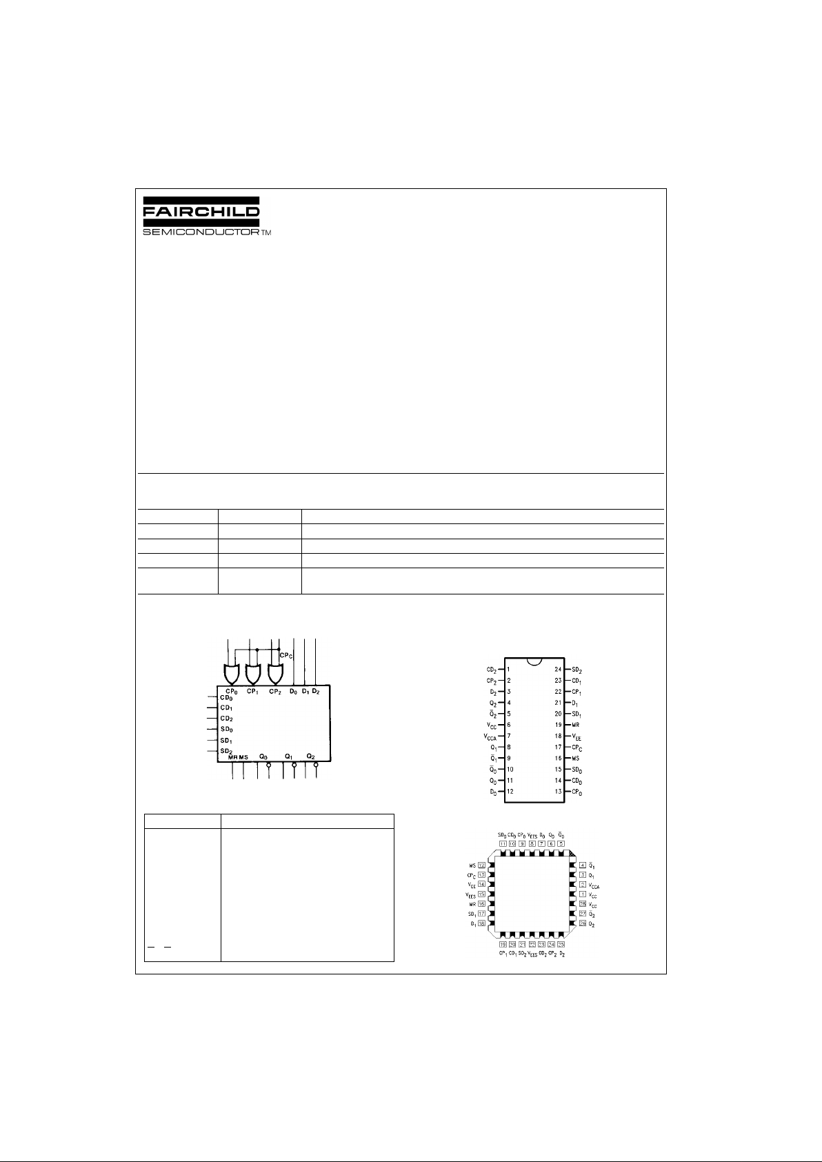
100331 Low Power Tri p le D-Type Flip-Flop
100331
Low Power Triple D-Type Flip-Flop
General Description
The 100331 contains three D-type, edge- triggered master/
slave flip-flops with true and complement outputs, a Common Clock (CP
C
), and Master Set (MS) an d Master Reset
(MR) inputs. Each flip-flop has individual Clock (CP
n
),
Direct Set (SD
n
) and Direct Clear (CDn) inputs. Data enters
a master when bot h CP
n
and CPC are LOW and tra nsfers
to a slave when CP
n
or CPC (or both) go HIGH. The Master
Set, Master Reset and individual CD
n
and SDn inputs over-
ride the Clock inputs. All inputs have 50 k
Ω pull-down
resistors.
Features
■ 35% power reduction of the 100131
■ 2000V ESD protection
■ Pin/function compatible with 100131
■ Voltage compensated operating range
= −4.2V to −5.7V
■ Available to industrial grade temperature range
Ordering Code:
Devices also availab le in Tape and Reel. Specify by appending th e s uffix let t er “X” to the ordering code.
Logic Symbol
Pin Descriptions
Connection Diagrams
24-Pin DIP/SOIC
28-Pin PLCC
Order Number Package Number Package Description
100331SC M24B 24-Lead Small Outline Integrated Circuit (SOIC), JEDEC MS-013, 0.300 Wide
100331PC N24E 24-Lead Plastic Dual-In-Line Package (PDIP), JEDEC MS-010, 0.400 Wide
100331QC V28A 28-Lead Plastic Lead Chip Carrier (PLCC), JEDEC MO-047, 0.450 Square
100331QI V28A 28-Lead Plastic Lead Chip Carrier (PLCC), JEDEC MO-047, 0.450 Square
Industrial Temperature Range (
−40°C to +85°C)
Pin Names Description
CP
0
–CP
2
Individual Clock Inputs
CP
C
Common Clock Input
D
0–D2
Data Inputs
CD
0
–CD
2
Individual Direct Clear Inputs
SD
n
Individual Direct Set Inputs
MR Master Reset Input
MS Master Set Input
Q
0-Q2
Data Outputs
Q
0–Q2
Complementary Data Outputs
Page 2
www.fairchildsemi.com 2
100331
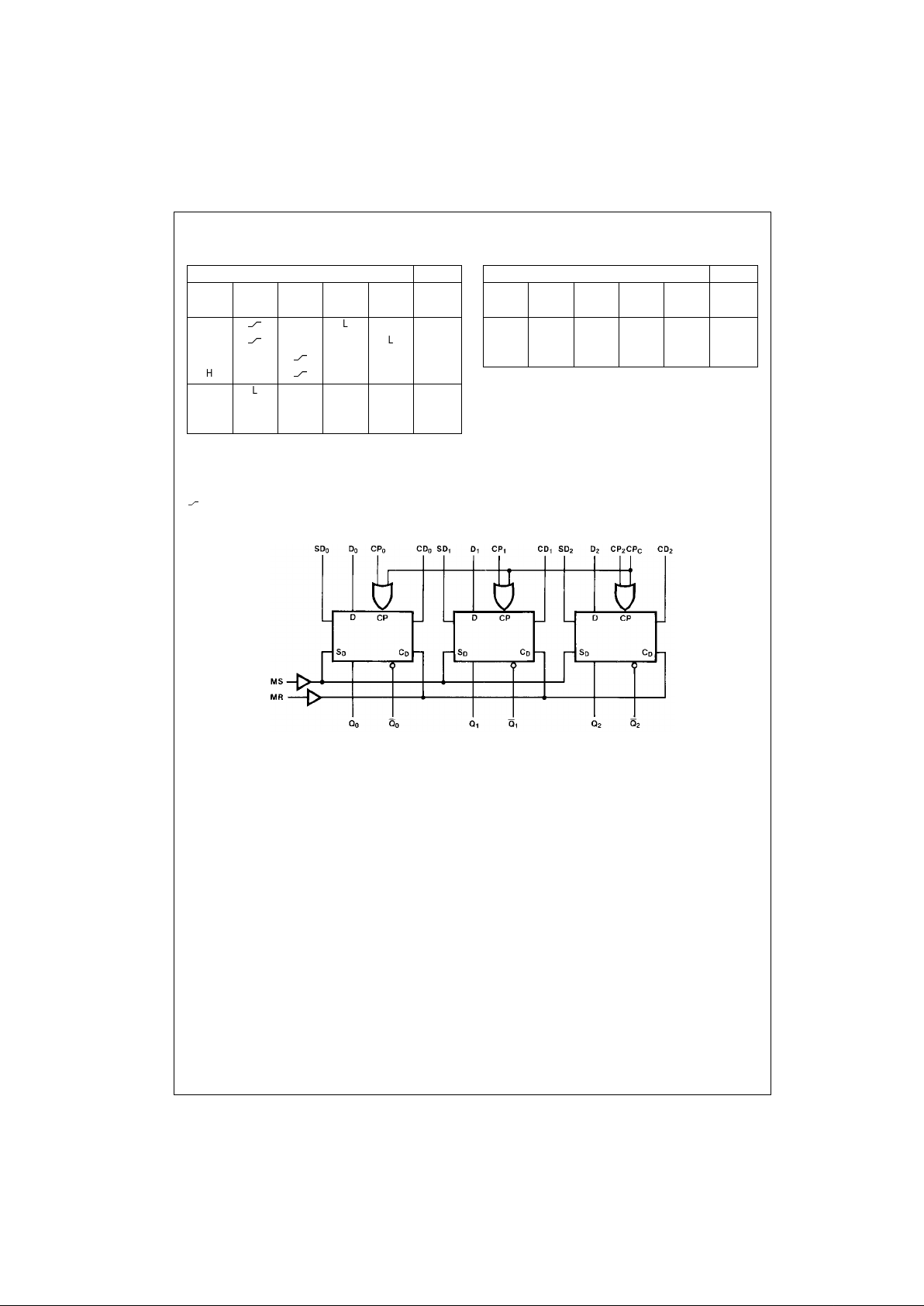
Truth Tables
H = HIGH Voltage Level
L = LOW Voltage Level
X = Don’t Care
U = Undefined
t = Time before CP Positive Transition
t + 1 = Time after CP Positive Tr ansition
= LOW-to-HIGH Transiti on
Logic Diagram
Synchronous Operation (Each Flip-Flop)
Inputs Outputs
D
n
CPnCP
C
MS MR
Q
n
(t + 1)
SD
n
CD
n
L
LLLL
H
LLLH
LL
LLL
HL
LLH
XLLLLQ
n
(t)
XHXLLQ
n
(t)
XXHLLQ
n
(t)
Asynchronous Operation (Each Flip-Flop)
Inputs Outputs
D
n
CPnCP
C
MS MR
Q
n
(t + 1)
SD
n
CD
n
XXXHLH
XXXLH L
XXXHHU
Page 3
3 www.fairchildsemi.com
100331
Absolute Maximum Ratings(Note 1) Recommended Operating
Conditions
Note 1: The “Absolute Maximum Ratings” are those value s beyond which
the safety of the dev ice cannot b e guaranteed . The device sh ould not be
operated at these limit s. The parametric values defi ned in the Electrical
Characteristics tables are not guaranteed at the absolute maximum rating.
The “Recomm ended O peratin g Cond itions ” table will defin e the condition s
for actual device operation.
Note 2: ESD testing conforms to MIL-STD-883, Method 3015.
Commercial Version
DC Electrical Characteristics
(Note 3)
V
EE
= −4.2V to −5.7V, VCC = V
CCA
= GND, T
C
= 0°C to +85°C
Note 3: The specified limits represent the “worst case” value for the parameter. Since these values normally occur at the temperature extremes, additional
noise immunity and guardbanding can be achieved by decreasin g the al l owable syste m opera ti ng ran ge s. Cond it i ons fo r t estin g sho w n in the tabl es are chosen to guarantee operation under “worst case” conditions.
Storage Temperature (T
STG
) −65°C to +150°C
Maximum Junction Temperature (T
J
) +150°C
Pin Potential to Ground Pin (V
EE
) −7.0V to +0.5V
Input Voltage (DC) V
EE
to +0.5V
Output Current
(DC Output HIGH)
−50 mA
ESD (Note 2)
≤ 2000V
Case Temperature (T
C
)
Commercial 0
°C to +85°C
Industrial
−40°C to +85°C
Supply Voltage (V
EE
) −5.7V to −4.2V
Symbol Parameter Min Typ Max Units Conditions
V
OH
Output HIGH Voltage −1025 −955 −870 mV VIN = VIH (Max) Loading with
V
OL
Output LOW Voltage −1830 −1705 −1620 mV or VIL (Min) 50Ω to −2.0V
V
OHC
Output HIGH Voltage −1035 mV VIN = VIH (Min) Loading with
V
OLC
Output LOW Voltage −1610 mV or VIL (Max) 50Ω to −2.0V
V
IH
Input HIGH Voltage −1165 −870 mV Guaranteed HIGH Signal
for All Inputs
V
IL
Input LOW Voltage −1830 −1475 mV Guaranteed LOW Signal
for All Inputs
I
IL
Input LOW Current 0.5 µAVIN = VIL (Min)
I
IH
Input HIGH Current 240 µAVIN = VIH (Max)
I
EE
Power Supply Current −122 −65 mA Inputs OPEN
Page 4

www.fairchildsemi.com 4
100331
Commercial Version (Continued)
DIP AC Electrical Characteristics
V
EE
= −4.2V to −5.7V, VCC = V
CCA
= GND
SOIC and PLCC AC Electrical Characteristics
V
EE
= −4.2V to −5.7V, VCC = V
CCA
= GND
Symbol Parameter
TC = 0°CT
C
= +25°CTC = +85°C
Units Conditions
Min Max Min Max Min Max
f
MAX
Toggle Frequency 375 375 375 MHz Figures 2, 3
t
PLH
Propagation Delay
0.75 2.00 0.75 2.00 0.75 2.00 ns
t
PHL
CPC to Output
Figures 1, 3
t
PLH
Propagation Delay
0.75 2.00 0.75 2.00 0.75 2.00 ns
t
PHL
CPn to Output
t
PLH
Propagation Delay
0.70 1.70 0.70 1.70 0.70 1.80 CPn, CPC = L
Figures 1, 4
t
PHL
CDn, SDn to Output
ns
t
PLH
0.70 2.00 0.70 2.00 0.70 2.00 CPn, CPC = H
t
PHL
t
PLH
Propagation Delay
1.10 2.60 1.10 2.60 1.10 2.60 CPn, CPC = L
t
PHL
MS, MR to Output
ns
t
PLH
1.10 2.80 1.10 2.80 1.10 2.80 CPn, CPC = H
t
PHL
t
TLH
Transition Time
0.35 1.30 0.35 1.30 0.35 1.30 ns Figures 1, 3, 4
t
THL
20% to 80%, 80% to 20%
t
S
Setup Time
Figure 5
D
n
0.40 0.40 0.40
ns
CDn, SDn (Release Time) 1.30 1.30 1.30
Figure 4
MS, MR (Release Time) 2.30 2.30 2.30
t
H
Hold Time D
n
0.5 0.5 0.7 ns Figure 5
tPW(H) Pulse Width HIGH
CPn, CPC, CDn, 2.00 2.00 2.00 ns Figures 3, 4
SDn, MR, MS
Symbol Parameter
TC = 0°CTC = +25°CTC = +85°C
Units Conditions
Min Max Min Max Min Max
f
MAX
Toggle Frequency 400 400 400 MHz Figures 2, 3
t
PLH
Propagation Delay
0.75 1.80 0.75 1.80 0.75 1.80 ns
t
PHL
CPC to Output
Figures 1, 3
t
PLH
Propagation Delay
0.75 1.80 0.75 1.80 0.75 1.80 ns
t
PHL
CPn to Output
t
PLH
Propagation Delay
0.70 1.50 0.70 1.50 0.70 1.60 CPn, CPC =L
Figures 1, 4
t
PHL
CDn, SDn to Output
ns
t
PLH
0.80 1.80 0.70 1.80 0.70 1.80 CPn, CPC = H
t
PHL
t
PLH
Propagation Delay
1.10 2.40 1.10 2.40 1.10 2.40 CPn, CPC = L
t
PHL
MS, MR to Output ns
t
PLH
1.10 2.60 1.10 2.60 1.10 2.60 CPn, CPC = H
t
PHL
t
TLH
Transition Time
0.35 1.10 0.35 1.10 0.35 1.10 ns Figures 1, 3, 4
t
THL
20% to 80%, 80% to 20%
t
S
Setup Time
Figure 5
D
n
0.30 0.30 0.30
CDn, SDn (Release Time) 1.20 1.20 1.20 ns
Figure 4
MS, MR (Release Time) 2.20 2.20 2.20
t
H
Hold Time D
n
0.5 0.5 0.7 ns Figure 5
tPW(H) Pulse Width HIGH
CPn, CPC, CDn, 2.00 2.00 2.00 ns Figures 3, 4
SDn, MR, MS
Page 5

5 www.fairchildsemi.com
100331
Commercial Version (Con tinu ed)
Note 4: Output-to-Output Skew is defined as the absolute value of the difference between the actual propagation delay for any outputs within the same pack-
aged device. The sp ecifica tions a pply to an y outp uts swit ching in the sam e direc tion eithe r HIGH -to-LOW (t
OSHL
), or LOW-to-HIGH (t
OSLH
), or in opposite
directions both HL and LH (t
OST
). Parameters t
OST
and tPS guaranteed by de s ign.
Symbol Parameter
T
C
= 0°CTC = +25°CTC = +85°C
Units Conditions
Min Max Min Max Min Max
t
PLH
Propagation Delay
0.75 1.40 0.75 1.40 0.80 1.50 ns
Figures 1, 3 PLCC Only
t
PHL
CPC to Output
t
PLH
Propagation Delay
0.70 1.40 0.75 1.40 0.80 1.50 ns
t
PHL
CPn to Output
t
PLH
Propagation Delay
0.70 1.50 0.70 1.50 0.80 1.60
CPn, CPC =L
Figures 1, 4
t
PHL
CDn, SDn to Output
ns
PLCC Only
t
PLH
0.80 1.70 0.80 1.70 0.80 1.80
CPn, CPC = H
t
PHL
PLCC Only
t
PLH
Propagation Delay
1.10 2.00 1.10 2.00 1.20 2.10
CPn, CPC = L
t
PHL
MS, MR to Output
ns
PLCC Only
t
PLH
1.20 2.10 1.20 2.10 1.30 2.20
CPn, CPC = H
t
PHL
PLCC Only
t
OSHL
Maximum Skew Common Edge PLCC Only
Output-to-Output Variation 100 100 100 ps (Note 4)
Common Clock to Output Path
t
OSHL
Maximum Skew Common Edge PLCC Only
Output-to-Output Variation 235 235 235 ps (Note 4)
CPn to Output Path
t
OSLH
Maximum Skew Common Edge PLCC Only
Output-to-Output Variation 120 120 120 ps (Note 4)
Common Clock to Output Path
t
OSLH
Maximum Skew Common Edge PLCC Only
Output-to-Output Variation 275 275 275 ps (Note 4)
CPn to Output Path
t
OST
Maximum Skew Opposite Edge ps PLCC Only
Output-to-Output Variation 125 125 125 (Note 4)
Common Clock to Output Path
t
OST
Maximum Skew Opposite Edge ps PLCC Only
Output-to-Output Variation 265 265 265 (Note 4)
CP
n
to Output Path
t
PS
Maximum Skew PLCC Only
Pin (Signal) Transition Variation 90 90 90 ps (Note 4)
Common Clock to Output Path
t
PS
Maximum Skew PLCC Only
Pin (Signal) Transition Variation 90 90 90 ps (Note 4)
CPn to Output Path
Page 6

www.fairchildsemi.com 6
100331
Industrial Version
PLCC DC Electrical Characteristics
(Note 5)
V
EE
= −4.2V to −5.7V, VCC = V
CCA
= GND, T
C
= −40°C to +85°C
Note 5: The specified limits represent the “worst case” value for the parameter. Since these values normally occur at the temperature extremes, additional
noise immunity and guardbanding can be achieved by decreasing the all owable syste m opera ti ng r ange s. Co ndi ti ons fo r t est ing shown in the ta ble s are chosen to guarantee operation under “worst case” conditions.
PLCC AC Electrical Characteristics
V
EE
= −4.2V to −5.7V, VCC = V
CCA
= GND
Symbol Parameter
T
C
= −40°CTC = 0°C to +85°C
Units Conditions
MinMaxMinMax
V
OH
Output HIGH Voltage −1085 −870 −1025 −870 mV VIN = VIH (Max) Loading with
V
OL
Output LOW Voltage −1830 −1575 −1830 −1620 mV or VIL (Min) 50Ω to −2.0V
V
OHC
Output HIGH Voltage −1095 −1035 mV VIN = VIH (Min) Loading with
V
OLC
Output LOW Voltage −1565 −1610 mV or VIL (Max) 50Ω to −2.0V
V
IH
Input HIGH Voltage −1170 −870 −1165 −870 mV Guaranteed HIGH Signal
for All Inputs
V
IL
Input LOW Voltage −1830 −1480 −1830 1475 mV Guaranteed LOW Signal
for All Inputs
I
IL
Input LOW Current 0.5 0.5 µAVIN = VIL (Min)
I
IH
Input HIGH Current 300 240 µAVIN = VIH (Max)
I
EE
Power Supply Current −122 −60 −122 −65 mA Inputs Open
Symbol Parameter
TC = −40°CTC = +25°CTC = +85°C
Units Conditions
Min Max Min Max Min Max
f
MAX
Toggle Frequency 375 400 400 MHz Figures 2, 3
t
PLH
Propagation Delay
0.75 1.80 0.75 1.80 0.75 1.80 ns
t
PHL
CPC to Output Figures 1, 3
t
PLH
Propagation Delay
0.70 1.80 0.75 1.80 0.75 1.80 ns
t
PHL
CPn to Output
t
PLH
Propagation Delay
0.60 1.50 0.70 1.50 0.70 1.60 CP
n
, CPC = L
Figures 1, 4
t
PHL
CDn, SDn to Output
ns
t
PLH
0.70 1.80 0.70 1.80 0.70 1.80 CPn, CPC = H
t
PHL
t
PLH
Propagation Delay
1.10 2.40 1.10 2.40 1.10 2.40 CPn, CPC = L
t
PHL
MS, MR to Output
ns
t
PLH
1.10 2.60 1.10 2.60 1.10 2.60 CPn, CPC = H
t
PHL
t
TLH
Transition Time
0.20 1.40 0.35 1.10 0.35
1.10
ns Figures 1, 3, 4
t
THL
20% to 80%, 80% to 20%
t
S
Setup Time
Figure 5
D
n
1.00 0.30 0.30
CDn,SDn(Release Time) 1.50 1.20 1.20 ns
Figure 4
MS, MR (Release Time) 2.50 2.20 2.20
t
H
Hold Time D
n
0.7 0.5 0.7 ns Figure 5
tPW(H) Pulse Width HIGH
CPn, CPC, CDn, 2.00 2.00 2.00 ns Figures 3, 4
SDn, MR, MS
Page 7

7 www.fairchildsemi.com
100331
Test Circuits
FIGURE 1. AC Test Circuit
Notes:
V
CC
, V
CCA
= +2V, VEE = −2.5V
L1 and L2 = Equal length 50Ω impedanc e lines
R
T
= 50Ω terminator internal to scope
Decouplin g 0.1 µF from GND to V
CC
and V
EE
All unused outputs are loaded with 50Ω to GND
C
L
= Fixture and stray capacitance ≤ 3 pF
FIGURE 2. Toggle Frequency Test Circuit
Page 8

www.fairchildsemi.com 8
100331
Switching Waveforms
FIGURE 3. Propagation Delay (Clock) and Transition Times
FIGURE 4. Propagation Delay (Resets)
FIGURE 5. Data Setup and Hold Time
Note:
t
S
is the minimum time before the transition of the clock that information must be present at the data input.
t
H
is the minimum time after the transition of the clock that information must remain unchanged at the data input.
Page 9

9 www.fairchildsemi.com
100331
Physical Dimensions inches (millimeters) unless otherwise noted
24-Lead Small Outline Integrated Circuit (SOIC), JEDEC MS-013, 0.300 Wide
Package Number M24B
24-Lead Plastic Dual-In-Line Package (PDIP), JEDEC MS-010, 0.400 Wide
Package Number N24E
Page 10

www.fairchildsemi.com 10
100331 Low Power Triple D-Type Flip-Flop
Physical Dimensions inches (millimeters) unless otherwise noted (Continued)
28-Lead Plastic Lead Chip Carrier (PLCC), JEDEC MO-047, 0.450 Square
Package Number V28A
Fairchild does not assume any responsibility for use of any circuitr y described, no circuit patent licenses are implied and
Fairchild reserves the right at any time without notice to change said circuitry and specifications.
LIFE SUPPORT POLICY
FAIRCHILD’S PRODUCTS ARE NOT AUTHORIZED FOR USE AS CRITICAL COMPONENTS IN LIFE SUPPORT
DEVICES OR SYSTEMS WITHOUT THE EXPRESS WRITTEN APPROVAL OF THE PRESIDENT OF FAIRCHILD
SEMICONDUCTOR CORPORATION. As used herein:
1. Life support devices or systems are devices or syste ms
which, (a) are intended for surgical implant into the
body, or (b) support or sustain life, and (c) whose failure
to perform when properly used in accordance with
instructions for use provided in the labeling, can be reasonably expected to result in a significant inju ry to the
user.
2. A critical component in any compon ent of a lif e supp ort
device or system whose failure t o perform can be reasonably expected to ca use the failure of the life supp ort
device or system, or to affect its safety or effectiveness.
www.fairchildsemi.com
 Loading...