

Datasheet 100329QI, 100329QCX, 100329QC, 100329PC, 100329DC Datasheet (Fairchild Semiconductor)
Page 1
© 2000 Fairchild Semiconductor Corporation DS010583 www.fairchildsemi.com
August 1989
Revised August 2000
100329 Low Power Octal ECL/TTL Bidirectional Translator with Register
100329
Low Power Octal ECL/TTL Bidirectional Translator
with Register
General Description
The 100329 is an octal reg istered bidirectional translator
designed to convert TTL logic levels to 100K ECL logic levels and vice versa. The dire ction of the translation is dete rmined by the DIR input. A LOW on the outp ut enable input
(OE) holds the ECL ou tputs in a cut- off state and the TTL
outputs at a high impedance level. The outputs change
synchronously with the r ising edge of the clock i nput (CP)
even though only one output is enabled at the time.
The cut-off state is designe d to be more negative than a
normal ECL LOW l evel. This allows the output emi tter-followers to turn off when the termination supply is
−2.0V, pre-
senting a high impedance to the data bus. This high
impedance reduces the termination power and prevents
loss of low state noise margin when several loads share
the bus.
The 100329 is designe d with FAST
TTL output buffers,
featuring optimal DC drive an d capabl e of quickly cha rging
and discharging highly capacitive loads. All inputs have
50 k
Ω pull-down resistors.
Features
■ Bidirectional translation
■ ECL high impedance outputs
■ Registered outputs
■ FAST TTL outputs
■ 3-STATE outputs
■ Voltage compensated operating range
= −4.2V to −5.7V
■ High drive IOS
Ordering Code:
Devices also availab le in Tape and Reel. Specify by appending su ffix let te r “X” to the ordering code.
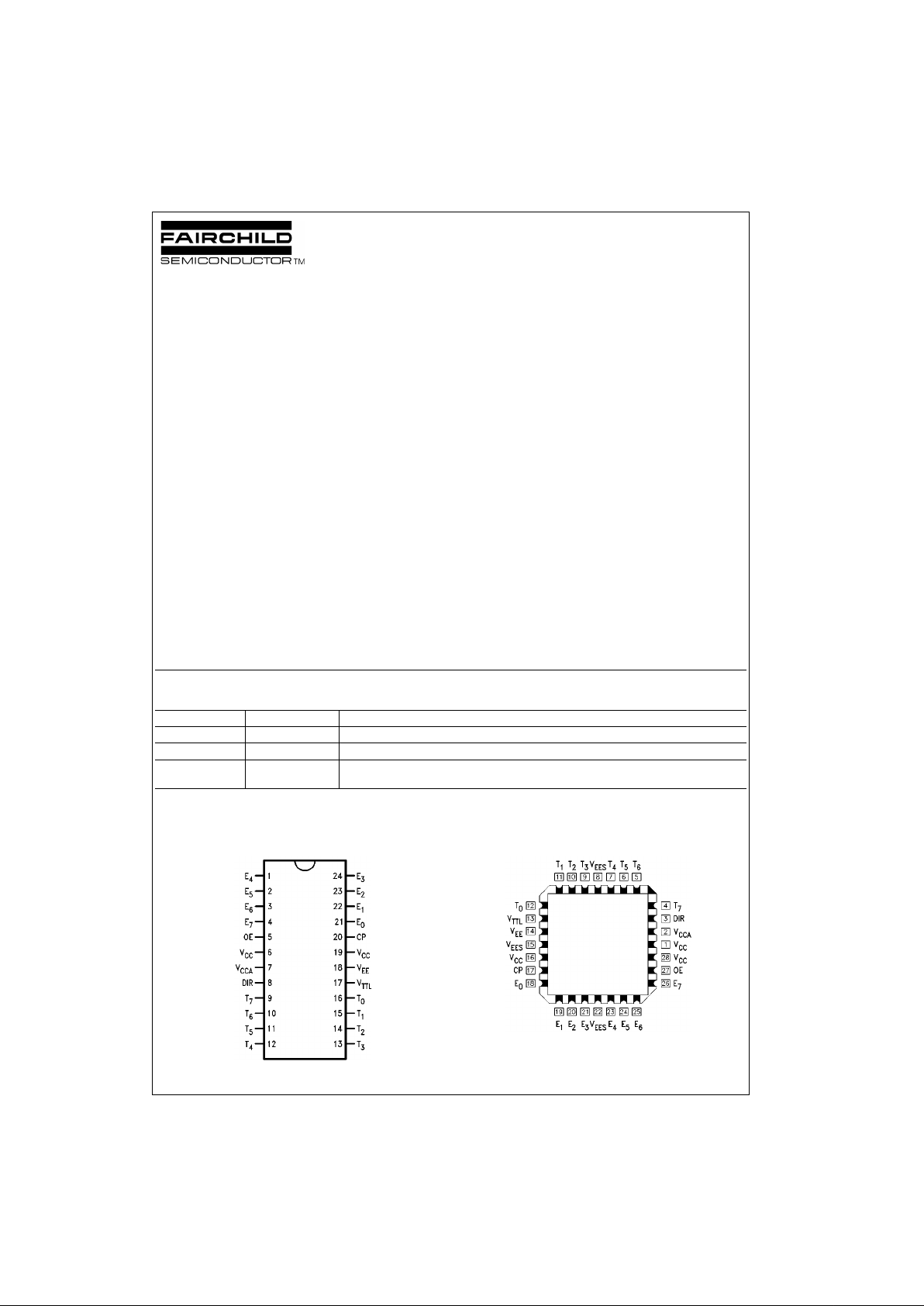
Connection Diagrams
24-Pin DIP 28-Pin PLCC
FAST is a registered trademark of Fairc hild Semiconductor Corporation.
Order Number Package Number Package Description
100329PC N24E 24-Lead Plastic Dual-In-Line Package (PDIP), JEDEC MS-010, 0.400 Wide
100329QC V28A 28-Lead Plastic Lead Chip Carrier (PLCC), JEDEC MO-047, 0.450 Square
100329QI V28A 28-Lead Plastic Lead Chip Carrier (PLCC), JEDEC MO-047, 0.450 Square
Industrial Temperature Range (
−40°C to +85°C)
Page 2
www.fairchildsemi.com 2
100329
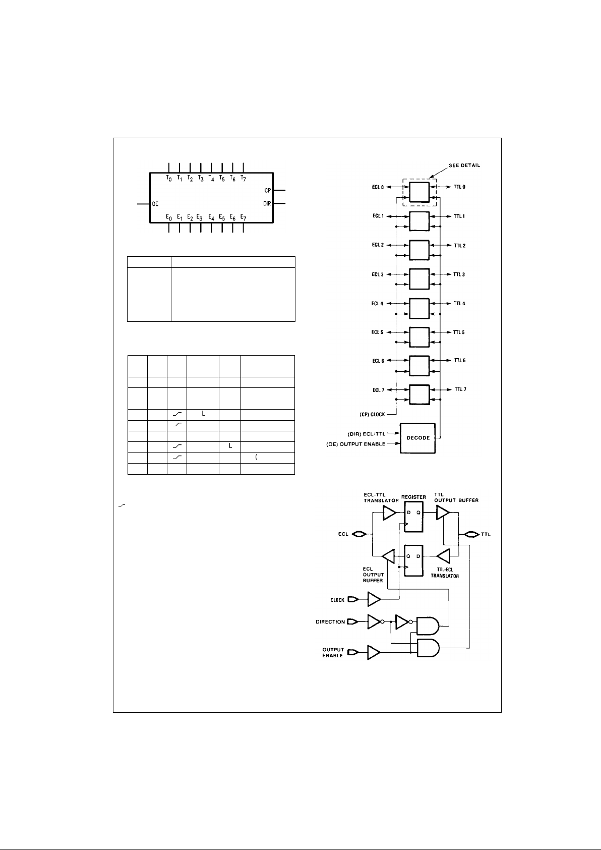
Logic Symbol
Pin Descriptions
All pins function at 100K ECL levels except fo r T0–T7.
Truth Table
H = HIGH Voltage Level
L = LOW Voltage Level
X = Don't Care
Z = High Impedance
= LOW-to-HIGH Clo c k Transi ti on
NC = No Change
Note 1: ECL input to TTL output mode.
Note 2: TTL input to ECL output mode.
Note 3: Retains data present before CP.
Functional Diagram
Note: DIR and OE use ECL logi c le v els
Detail
Pin Names Description
E
0–E7
ECL Data I/O
T
0–T7
TTL Data I/O
OE Output Enable Input
CP Clock Pulse Input (Active Rising Edge)
DIR Direction Control Input
OE DIR CP
ECL TTL
Notes
Port Port
L L X Input Z (Note 1)(Note 3)
L H X LOW Input (Note 2)(Note 3)
(Cut-Off )
H L
L L (Note 1)
H L
H H (Note 1)
H L L X NC (Note 1)(Note 3)
H H
L L (Note 2)
H H
H H (Note 2)
H H L NC X (Note 2)(Note 3)
Page 3
3 www.fairchildsemi.com
100329
Absolute Maximum Ratings(Note 4) Recommended Operating
Conditions
Note 4: The “Absolute Maximum Ratings” are those value s beyond which
the safety of the dev ice cannot b e guaranteed . The device sh ould not be
operated at these limit s. The parametric values defi ned in the Electrical
Characteristics tables are not guaranteed at the absolute maximum rating.
The “Recomm ended O peratin g Cond itions ” table will defin e the condition s
for actual device operation.
Note 5: ESD testing conforms to MIL-STD-883, Method 3015.
Note 6: Either voltage lim it or c urrent limit is sufficient to pro te c t in puts.
TTL-to-ECL DC Electrical Characteristics
V
EE
= −4.2V to −5.7V, VCC = V
CCA
= GND, TC = 0°C to +85°C, V
TTL
= +4.5V to +5.5V (Note 7)
Note 7: The specified limits represent the “worst case” value for the parameter. Since these values normally occur at the temperature extremes, additional
noise immunity and guardbanding can be achieved by decreasin g the al l owable syste m opera ti ng ran ge s. Cond it i ons fo r t estin g sho w n in the tabl es are chosen to guarantee operation under “worst case” conditions.
Storage Temperature (T
STG
) −65°C to +150°C
Maximum Junction Temperature (T
j
) +150°C
V
EE
Pin Potential to Ground Pin −7.0V to +0.5V
V
TTL
Pin Potential to Ground Pin −0.5V to +6.0V
ECL Input Voltage (DC) V
EE
to +0.5V
ECL Output Current
(DC Output HIGH)
−50 mA
TTL Input Voltage (Note 6)
−0.5V to +6.0V
TTL Input Current (Note 6)
−30 mA to +5.0 mA
Voltage Applied to Output
in HIGH State
3-STATE Output
−0.5V to +5.5V
Current Applied to TTL
Output in LOW State (Max) twice the rated I
OL
(mA)
ESD (Note 5)
≥2000V
Case Temperature (T
C
)0°C to +85°C
ECL Supply Voltage (V
EE
) −5.7V to −4.2V
TTL Supply Voltage (V
TTL
) +4.5V to +5.5V
Symbol Parameter Min Typ Max Units Conditions
V
OH
Output HIGH Voltage −1025 −955 −870 mV VIN = VIH (Max) or VIL (Min)
V
OL
Output LOW Voltage −1830 −1705 −1620 mV Loading with 50Ω to −2V
Cutoff Voltage OE or DIR LOW,
−2000 −1950 mV VIN = VIH (Max) or VIL (Min)
Loading with 50Ω to −2V
V
OHC
Output HIGH Voltage
−1035
mV
Corner Point HIGH V
IN
= VIH (Min) or VIL (Max)
V
OLC
Output LOW Voltage
−1610 mV
Loading with 50Ω to −2V
Corner Point LOW
V
IH
Input HIGH Voltage 2.0 5.0 V Over V
TTL
, VEE, TC Range
V
IL
Input LOW Voltage 0 0.8 V Over V
TTL
, VEE, TC Range
I
IH
Input HIGH Current 70 µAVIN = +2.7V
Breakdown Test 1.0 mA V
IN
= +5.5V
I
IL
Input LOW Current −700 µAVIN = +0.5V
V
FCD
Input Clamp
−1.2 V I
IN
= −18 mA
Diode Voltage
I
EE
VEE Supply Current LE LOW, OE and DIR HIGH
Inputs Open
−189 −94 mA VEE = −4.2V to −4.8V
−199 −94 VEE = −4.2V to −5.7V
Page 4
www.fairchildsemi.com 4
100329
ECL-to-TTL DC Electrical Characteristics
V
EE
= −4.2V to −5.7V, VCC = V
CCA
= GND, TC = 0°C to +85°C, CL = 50 pF, V
TTL
= +4.5V to +5.5V (Note 8)
Note 8: The specified limits represent the “worst case” value for the parameter. Since these values normally occur at the temperature extremes, additional
noise immunity and guardbanding can be achieved by decreasing the all owable syste m opera ti ng r ange s. Co ndi ti ons fo r t est ing shown in the ta ble s are chosen to guarantee operation under “worst case” conditions.
DIP TTL-to-ECL AC Electrical Characteristics
V
EE
= −4.2V to −5.7V, V
TTL
= +4.5V to +5.5V, VCC = V
CCA
= GND
Symbol Parameter Min Typ Max Units Conditions
V
OH
Output HIGH Voltage 2.7 3.1 V IOH = −3 mA, V
TTL
= 4.75V
2.4 2.9 V I
OH
= −3 mA, V
TTL
= 4.50V
V
OL
Output LOW Voltage 0.3 0.5 V IOL = 24 mA, V
TTL
= 4.50V
V
IH
Input HIGH Voltage −1165 −870 mV Guaranteed HIGH Signal
for All Inputs
V
IL
Input LOW Voltage −1830 −1475 mV Guaranteed LOW Signal
for All Inputs
I
IH
Input HIGH Current 350 µAVIN = VIH (Max)
I
IL
Input LOW Current 0.50 µAVIN = VIL (Min)
I
OZHT
3-STATE Current 70 µAV
OUT
= +2.7V
Output HIGH
I
OZLT
3-STATE Current −700 µAV
OUT
= +0.5V
Output LOW
I
OS
Output Short-Circuit −225 −100 mA V
OUT
= 0.0V, V
TTL
= +5.5V
Current
I
TTL
V
TTL
Supply Current 74 mA TTL Outputs LOW
49 mA TTL Outputs HIGH
67 mA TTL Outputs in 3-STATE
Symbol Parameter
TC = 0°CT
C
= 25°CT
C
= 85°C
Units Conditions
MinMaxMinMaxMinMax
f
MAX
Max Toggle Frequency 350 350 350 MHz
t
PLH
CP to E
n
1.7 3.6 1.7 3.7 1.9 3.9 ns Figures 1, 2
t
PHL
t
PZH
OE to E
n
1.3 4.2 1.5 4.4 1.7 4.8 ns Figures 1, 2
(Cutoff to HIGH)
t
PHZ
OE to E
n
1.5 4.5 1.6 4.5 1.6 4.6 ns Figures 1, 2
(HIGH to Cutoff)
t
PHZ
DIR to E
n
1.6 4.3 1.6 4.3 1.7 4.5 ns Figures 1, 2
(HIGH to Cutoff)
t
SET
Tn to CP 1.1 1.1 1.1 ns Figures 1, 2
t
HOLD
Tn to CP 1.7 1.7 1.9 ns Figures 1, 2
tPW(H) Pulse Width CP 2.1 2.1 2.1 ns Figures 1, 2
t
TLH
Transition Time 0.6 1.6 0.6 1.6 0.6 1.6 ns Figures 1, 2
t
THL
20% to 80%, 80% to 20%
Page 5

5 www.fairchildsemi.com
100329
DIP ECL-to-TTL AC Electrical Characteristics
V
EE
= −4.2V to −5.7V, V
TTL
= +4.5V to +5.5V, VCC = V
CCA
= GND, C
L
= 50 pF
PLCC and TTL-to-ECL AC Electrical Characteristics
V
EE
= −4.2V to −5.7V, V
TTL
= +4.5V to +5.5V
Note 9: Output-to-Output Skew is defined as the absolute value of the difference between the actual propagation delay for any outputs within the same packaged device. The sp ecifica tions a pply to an y outp uts swit ching in the sam e direc tion eithe r HIGH -to-LOW (t
OSHL
), or LOW-to-HIGH (t
OSLH
), or in opposite
directions both HL and LH (t
OST
). Parameters t
OST
and tPS guaranteed by de s ign.
Symbol Parameter
T
C
= 0°CT
C
= 25°CT
C
= 85°C
Units Conditions
Min Max Min Max Min Max
f
MAX
Max Toggle Frequency 125 125 125 MHz
t
PLH
CP to T
n
3.1 7.2 3.1 7.2 3.3 7.7 ns Figures 3, 4
t
PHL
t
PZH
OE to T
n
3.4 8.45 3.7 8.95 4.0 9.7
ns Figures 3, 5
t
PZL
(Enable Time) 3.8 9.2 4.0 9.2 4.3 9.95
t
PHZ
OE to T
n
3.2 8.95 3.3 8.95 3.5 9.2
ns Figures 3, 5
t
PLZ
(Disable Time) 3.0 7.7 3.4 8.7 4.1 9.95
t
PHZ
DIR to T
n
2.7 8.2 2.8 8.7 3.1 8.95
ns Figures 3, 6
t
PLZ
(Disable Time) 2.8 7.45 3.1 7.95 4.0 9.2
t
SET
En to CP 1.1 1.1 1.1 ns Figures 3, 4
t
HOLD
En to CP 2.1 2.1 2.6 ns Figures 3, 4
tPW(H) Pulse Width CP 4.1 4.1 4.1 ns Figures 3, 4
Symbol Parameter
TC = 0°CT
C
= 25°CT
C
= 85°C
Units Conditions
Min Max Min Max Min Max
f
MAX
Max Toggle Frequency 350 350 350 MHz
t
PLH
CP to E
n
1.7 3.4 1.7 3.5 1.9 3.7 ns Figures 1, 2
t
PHL
t
PZH
OE to E
n
1.3 4.0 1.5 4.2 1.7 4.6 ns Figures 1, 2
(Cutoff to HIGH)
t
PHZ
OE to E
n
1.5 4.3 1.6 4.3 1.6 4.4 ns Figures 1, 2
(HIGH to Cutoff)
t
PHZ
DIR to E
n
1.6 4.1 1.6 4.1 1.7 4.3 ns Figures 1, 2
(HIGH to Cutoff)
t
SET
Tn to CP 1.0 1.0 1.0 ns Figures 1, 2
t
HOLD
Tn to CP 1.7 1.7 1.9 ns Figures 1, 2
t
PW
(H) Pulse Width CP 2.0 2.0 2.0 ns Figures 1, 2
t
TLH
Transition Time 0.6 1.6 0.6 1.6 0.6 1.6 ns Figures 1, 2
t
THL
20% to 80%, 80% to 20%
t
OSHL
Maximum Skew Common Edge PLCC Only
Output-to-Output Variation 200 200 200 ps (Note 9)
Data to Output Path
t
OSLH
Maximum Skew Common Edge PLCC Only
Output-to-Output Variation 200 200 200 ps (Note 9)
Data to Output Path
t
OST
Maximum Skew Opposite Edge PLCC Only
Output-to-Output Variation 650 650 650 ps (Note 9)
Data to Output Path
t
PS
Maximum Skew PLCC Only
Pin (Signal) Transition Variation 650 650 650 ps (Note 9)
Data to Output Path
Page 6

www.fairchildsemi.com 6
100329
PLCC and ECL-to-TTL AC Electrical Characteristics
V
EE
= −4.2V to −5.7V, V
TTL
= +4.5V to +5.5V, C
L
= 50 pF
Note 10: Output-to-Output Skew is defined as the absolute value of the difference between the actual propagation delay for any outputs within the same
packaged devic e. T he specifications ap ply to any outputs sw it c hing in the same direc t ion either HIGH-to-LOW (t
OSHL
), or LOW-to-HIGH (t
OSLH
), or in oppo-
site directions bot h H L and LH (t
OST
). Parameters t
OST
and tPS guaranteed by design.
Symbol Parameter
T
C
= 0°CT
C
= 25°CT
C
= 85°C
Units Conditions
Min Max Min Max Min Max
f
MAX
Max Toggle Frequency 125 125 125 MHz
t
PLH
CP to T
n
3.1 7.0 3.1 7.0 3.3 7.5 ns Figures 3, 4
t
PHL
t
PZH
OE to T
n
3.4 8.25 3.7 8.75 4.0 9.5 ns Figures 3, 5
t
PZL
(Enable Time) 3.8 9.0 4.0 9.0 4.3 9.75
t
PHZ
OE to T
n
3.2 8.75 3.3 8.75 3.5 9.0 ns Figures 3, 5
t
PLZ
(Disable Time) 3.0 7.5 3.4 8.5 4.1 9.75
t
PHZ
DIR to T
n
2.7 8.0 2.8 8.5 3.1 8.75 ns Figures 3, 6
t
PLZ
(Disable Time) 2.8 7.25 3.1 7.75 4.0 9.0
t
SET
En to CP 1.0 1.0 1.0 ns Figures 3, 4
t
HOLD
En to CP 2.0 2.0 2.5 ns Figures 3, 4
tPW(H) Pulse Width CP 4.0 4.0 4.0 ns Figures 3, 4
t
OSHL
Maximum Skew Common Edge PLCC Only
Output-to-Output Variation 600 600 600 ps (Note 10)
Data to Output Path
t
OSLH
Maximum Skew Common Edge PLCC Only
Output-to-Output Variation 850 850 850 ps (Note 10)
Data to Output Path
t
OST
Maximum Skew Opposite Edge PLCC Only
Output-to-Output Variation 1350 1350 1350 ps (Note 10)
Data to Output Path
t
PS
Maximum Skew PLCC Only
Pin (Signal) Transition Variation 950 950 950 ps (Note 10)
Data to Output Path
Page 7

7 www.fairchildsemi.com
100329
Test Circuitry (TTL-to-ECL)
Note 11: RT = 50Ω termination resistive load. When an input or output is being monitored by a scope, RTis supplied by th e scope’s 50Ω input resistance.
When an input or output is not being monitored, an ex te rnal 50Ω resistance must be applied to serve as R
T
.
Note 12: TTL and ECL force signals are brought to the DUT via 50Ω coax lines.
Note 13: V
TTL
is decoupled to ground w it h 0.1 µF, VEE is decoupled to ground with 0.01 µF and VCC is connected to ground.
FIGURE 1. TTL-to-ECL AC Test Circuit
Switching Waveforms (TTL-to-ECL)
FIGURE 2. TTL to ECL Transition—Propagation Delay and Transition Times
Page 8

www.fairchildsemi.com 8
100329
Test Circuitry (ECL-to-TTL)
Note 14: RT = 50Ω termination resistive load. When an input or output is being monitored by a scope, RT is supplied by the scope’s 50Ω input resistance.
When an input or ou tp ut is not being monitored, an ex te rnal 50Ω resistance must be applied to serve as R
T
.
Note 15: The TTL 3-STATE pull-up switch is connecte d t o +7V only for ZL and LZ tests.
Note 16: TTL and ECL force signals are brought to the DUT via 50Ω coax lines.
Note 17: V
TTL
is decoupled to ground with 0.1 µF, VEE is decoupled to ground w it h 0.01 µF and VCC is connected to ground.
FIGURE 3. ECL-to-TTL AC Test Circuit
Page 9

9 www.fairchildsemi.com
100329
Switching Waveforms (ECL-to-TTL)
Note: DIR is LOW, OE is HIGH
FIGURE 4. ECL-to-TTL Transition—Propagation Delay and Transition Times
Note: DIR is LOW
FIGURE 5. ECL-to-TTL T ransition, OE to TTL Output, Enable and Disable Times
Note: OE is HIGH
FIGURE 6. ECL-to-TTL Transition, DIR to TTL Output, Disable Time
Page 10

www.fairchildsemi.com 10
100329
Physical Dimensions inches (millimeters) unless otherwise noted
24-Lead Plastic Dual-In-Line Package (PDIP), JEDEC MS-010, 0.400 Wide
Package Number N24E
Page 11

11 www.fairchildsemi.com
100329 Low Power Octal ECL/TTL Bidirectional Translator with Register
Physical Dimensions inches (millimeters) unless otherwise noted (Continued)
28-Lead Plastic Lead Chip Carrier (PLCC), JEDEC MO-047, 0.450 Square
Package Number V28A
Fairchild does not assume any responsibility for use of any circuitry described , no circuit patent licenses are implied and
Fairchild reserves the right at any time without notice to change said circuitry and specifications.
LIFE SUPPORT POLICY
FAIRCHILD’S PRODUCTS ARE NOT AUTHORIZED FOR USE AS CRITICAL COMPONENTS IN LIFE SUPPORT
DEVICES OR SYSTEMS WITHOUT THE EXPRESS WRITTEN APPROVAL OF THE PRESIDENT OF FAIRCHILD
SEMICONDUCTOR CORPORATION. As used herein:
1. Life support devices or systems are devices or systems
which, (a) are intended for surgical implant into the
body, or (b) support or sustain life, and (c) whose failure
to perform when properly used in accordance with
instructions for use provide d in the labe l ing, can be re asonably expected to result in a significant injury to the
user.
2. A critical component in any compo nent o f a li fe supp ort
device or system whose failure to perform can be reasonably expected to cause the failure of the l ife support
device or system, or to affect its safety or effectiveness.
www.fairchildsemi.com
 Loading...