

Page 1
100328
Low Power Octal ECL/TTL Bi-Directional Translator with
Latch
General Description
The 100328 is an octal latched bi-directional translator designed to convert TTL logic levels to 100K ECL logic levels
and vice versa.Thedirectionof this translation is determined
by the DIR input. A LOW on the output enable input (OE)
holds the ECL outputs in a cut-off state and the TTL outputs
at a high impedance level. A HIGH on the latch enable input
(LE) latches the data at both inputs even though only one
output is enabled at the time. A LOW on LE makes the
100328 transparent.
The cut-off state is designed to be more negative than a normal ECL LOW level. This allows the output emitter-followers
to turn off when the termination supply is −2.0V,presenting a
high impedance to the data bus. This high impedance reduces termination power and prevents loss of low state
noise margin when several loads share the bus.
The 100328 is designed with FAST
®
TTL output buffers, featuring optimal DC drive and capable of quickly charging and
discharging highly capacitive loads. All inputs have 50 kΩ
pull-down resistors.
Features
n Identical performance to the 100128 at 50%of the
supply current
n Bi-directional translation
n 2000V ESD protection
n Latched outputs
n FAST TTL outputs
n TRI-STATE
®
outputs
n Voltage compensated operating range
=
−4.2V to −5.7V
n Available to MIL-STD-883
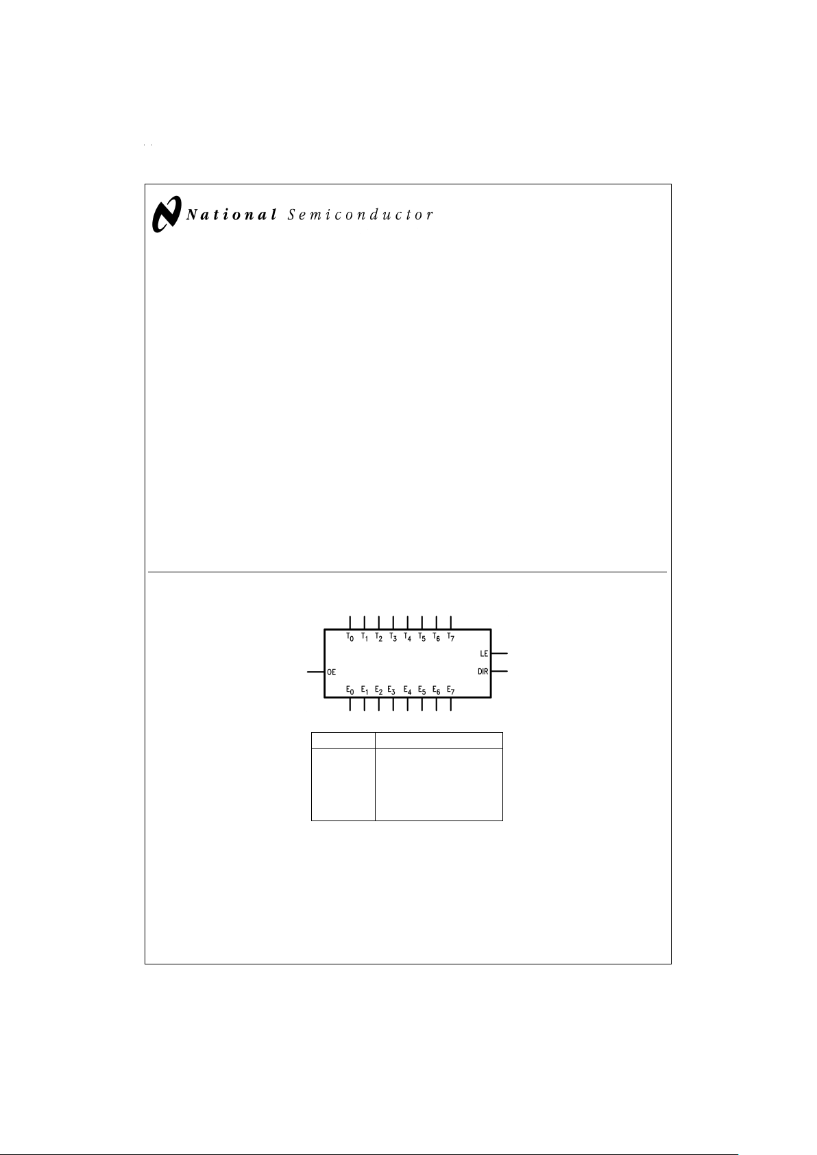
Logic Symbol
Pin Names Description
E
0–E7
ECL Data I/O
T
0–T7
TTL Data I/O
OE Output Enable Input
LE Latch Enable Input
DIR Direction Control Input
All pins function at 100K ECL levels except for T0–T7.
TRI-STATE®is a registered trademark of National Semiconductor Corporation.
FAST
®
is a registered trademark of Fairchild Semiconductor.
DS100295-1
August 1998
100328 Low Power Octal ECL/TTL Bi-Directional Translator with Latch
© 1998 National Semiconductor Corporation DS100295 www.national.com
Page 2
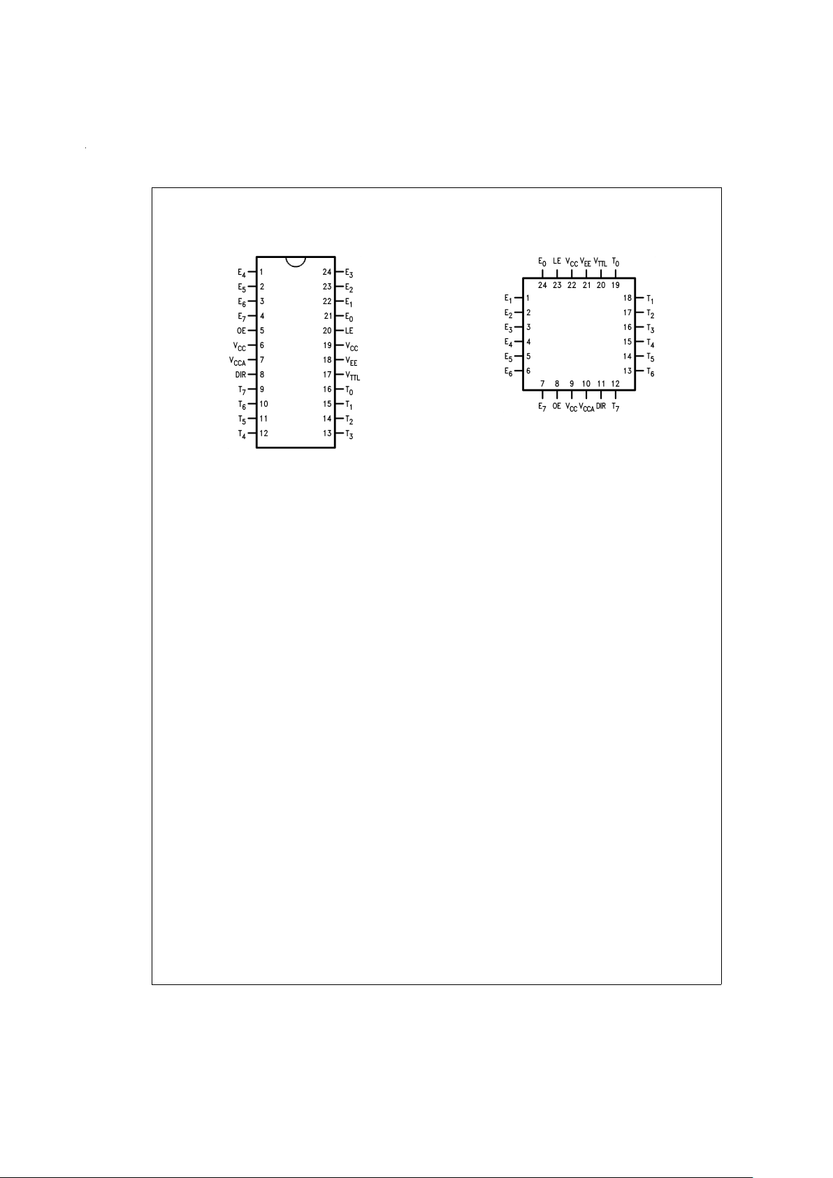
Connection Diagrams
24-Pin DIP
DS100295-2
24-Pin Quad Cerpak
DS100295-4
www.national.com 2
Page 3
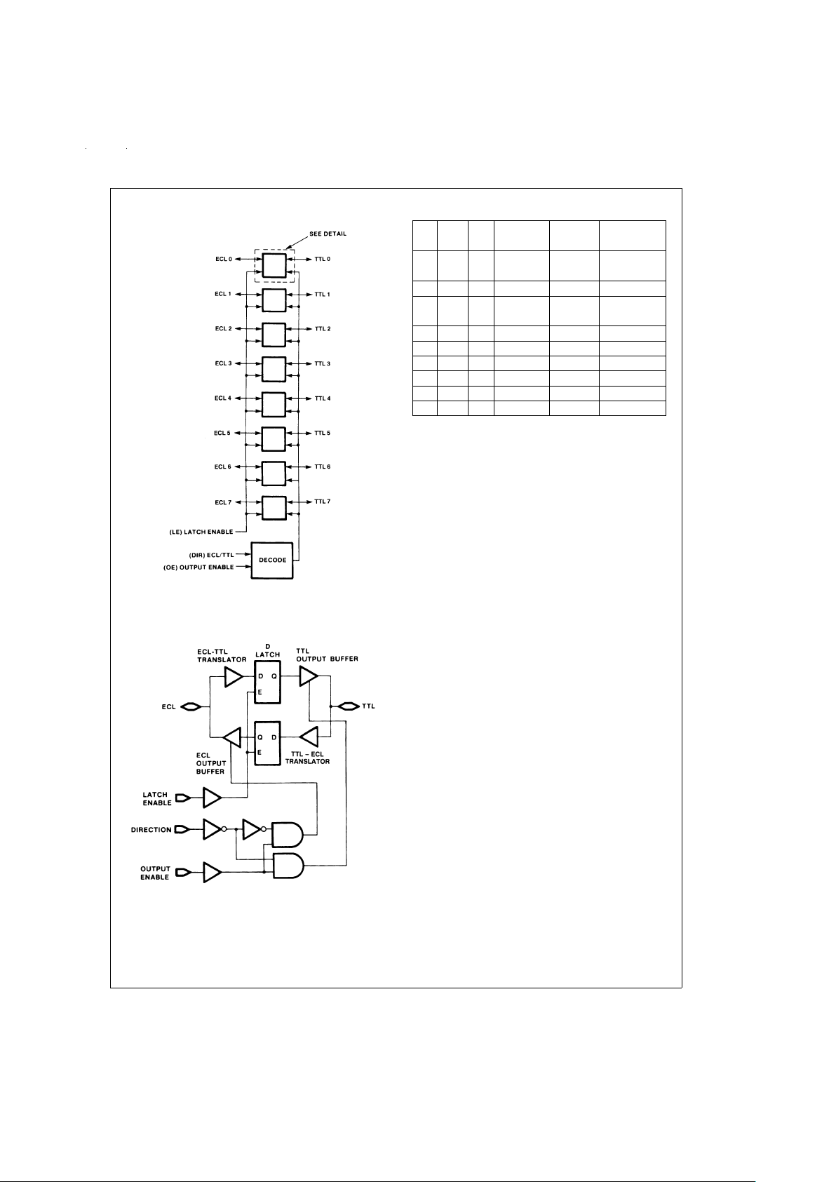
Functional Diagram
Detail
Truth Table
OE DIR LE ECL TTL Notes
Port Port
L X L LOW Z
(Cut-Off)
L L H Input Z (Notes 1, 3)
L H H LOW Input (Notes 2, 3)
(Cut-Off)
H L L L L (Notes 1, 4)
H L L H H (Notes 1, 4)
H L H X Latched (Notes 1, 3)
H H L L L (Notes 2, 4)
H H L H H (Notes 2, 4)
H H H Latched X (Notes 2, 4)
H=HIGH Voltage Level
L=LOW Voltage Level
X=Don’t Care
Z=High Impedance
Note 1: ECL input to TTL output mode.
Note 2: TTL input to ECL output mode.
Note 3: Retains data present before LE set HIGH.
Note 4: Latch is transparent.
DS100295-5
Note: LE, DIR, and OE use ECL logic levels
DS100295-6
www.national.com3
Page 4
Absolute Maximum Ratings (Note 5)
If Military/Aerospace specified devices are required,
please contact the National Semiconductor Sales Office/
Distributors for availability and specifications.
Storage Temperature (T
STG
) −65˚C to +150˚C
Maximum Junction Temperature (T
J
)
Ceramic +175˚C
V
EE
Pin Potential to
Ground Pin −7.0V to +0.5V
V
TTL
Pin Potential to
Ground Pin −0.5V to +6.0V
ECL Input Voltage (DC) V
EE
to +0.5V
ECL Output Current
(DC Output HIGH) −50 mA
TTL Input Voltage (Note 7) −0.5V to +6.0V
TTL Input Current (Note 7) −30 mA to +5.0 mA
Voltage Applied to Output in HIGH State
TRI-STATE Output −0.5V to +5.5V
Current Applied to TTL
Output in LOW State (Max) Twice the Rated I
OL
(mA)
ESD (Note 6) ≥2000V
Recommended Operating
Conditions
Case Temperature (TC)
Military −55˚C to +125˚C
ECL Supply Voltage (V
EE
) −5.7V to −4.2V
TTL Supply Voltage (V
TTL
) +4.5V to +5.5V
Note 5: Absolute maximum ratings are those values beyond which the device may be damaged or have its useful life impaired. Functional operation
under these conditions is not implied.
Note 6: ESD testing conforms to MIL-STD-883, Method 3015.
Note 7: Either voltage limit or current limit is sufficient to protect inputs.
Military Version
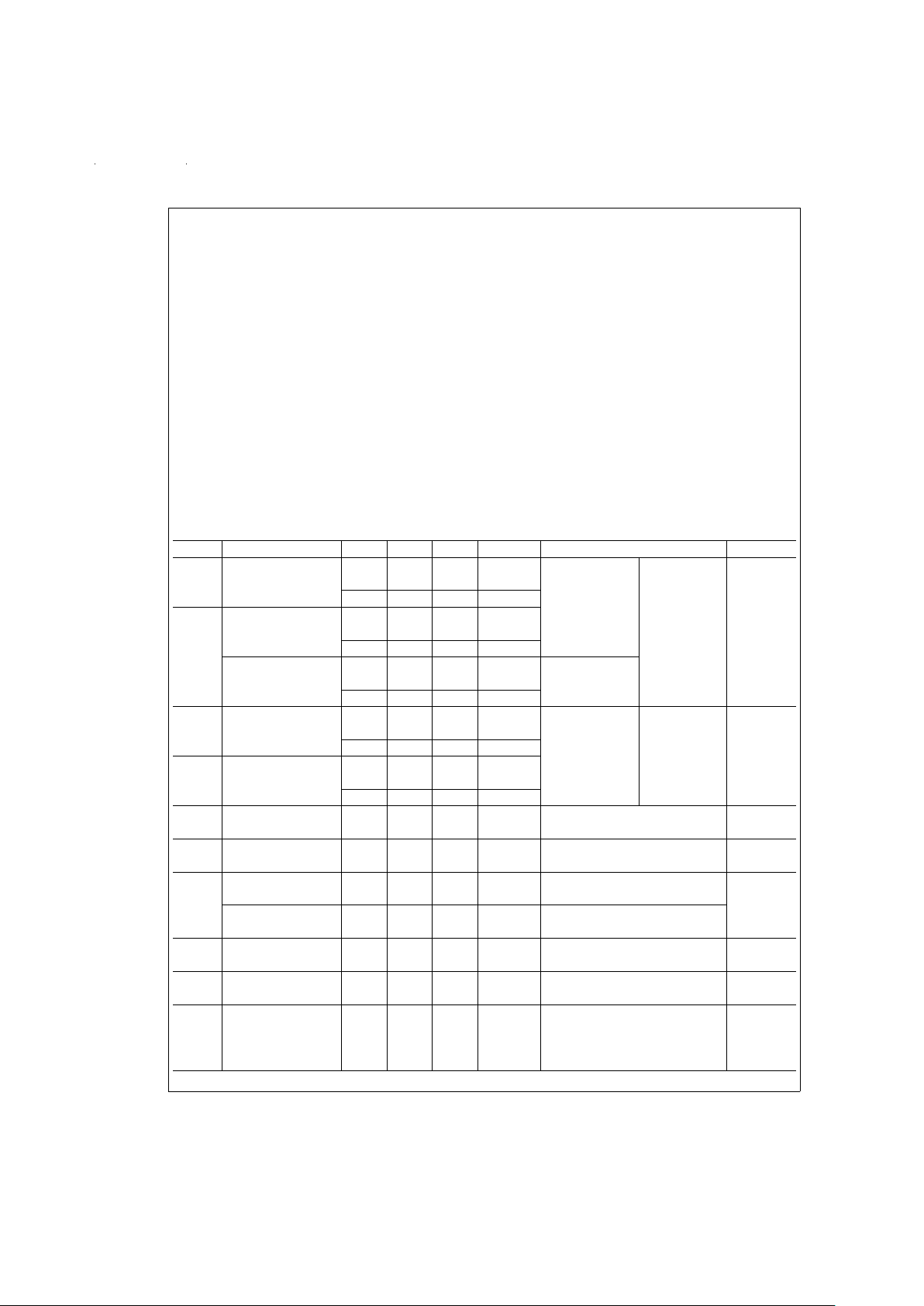
TTL-to-ECL DC Electrical Characteristics
V
EE
=
−4.2V to −5.7V, V
CC
=
V
CCA
=
GND, T
C
=
−55˚C to +125˚C, V
TTL
=
+4.5V to +5.5V
Symbol Parameter Min Max Units T
C
Conditions Notes
V
OH
Output HIGH Voltage −1025 −870 mV 0˚C to Loading with
50Ω to −2.0V
(Notes 8, 9,
10)
+125˚C
−1085 −870 mV −55˚C V
IN
=
V
IH
(Max)
V
OL
Output LOW Voltage −1830 −1620 mV 0˚C to or VIL(Min)
+125˚C
−1830 −1555 mV −55˚C
Cutoff Voltage −1950 mV 0˚C to
+125˚C OE or DIR Low
−1850 mV −55˚C
V
OHC
Output HIGH Voltage −1035 mV 0˚C to (Notes 8, 9,
10)
+125˚C
−1085 mV −55˚C V
IN
=
V
IH
(Min) Loading with
V
OLC
Output LOW Voltage −1610 mV 0˚C to or VIL(Max) 50Ω0 to −2.0V
+125˚C
−1555 mV −55˚C
V
IH
Input HIGH Voltage 2.0 V −55˚C to Over V
TTL,VEE,TC
Range (Notes 8, 9,
10, 11)
+125˚C
V
IL
Input LOW Voltage 0.8 V −55˚C to Over V
TTL,VEE,TC
Range (Notes 8, 9,
10, 11)
+125˚C
I
IH
Input HIGH Current 70 µA −55˚C to V
IN
=
+2.7V (Notes 8, 9,
10)
125˚C
Breakdown Test 1.0 mA −55˚C to V
IN
=
+5.5V
+125˚C
I
IL
Input LOW Current −1.0 mA −55˚C to V
IN
=
+0.5V (Notes 8, 9,
10)
+125˚C
V
FCD
Input Clamp −1.2 V −55˚C to I
IN
=
−18 mA (Notes 8, 9,
10)
Diode Voltage +125˚ C
I
EE
VEESupply Current LE Low, OE and DIR High (Notes 8, 9,
10)
−55˚C to Inputs Open
−165 −73 mA +125˚C V
EE
=
−4.2V to −4.8V
−175 −73 V
EE
=
−4.2V to −5.7V
www.national.com 4
Page 5

Military Version
ECL-to-TTL DC Electrical Characteristics
V
EE
=
−4.2V to −5.7V, V
CC
=
V
CCA
=
GND, T
C
=
−55˚C to +125˚C, C
L
=
50 pF, V
TTL
=
+4.5V to + 5.5V
Symbol Parameter Min Max Units T
C
Conditions Notes
V
OH
Output HIGH Voltage 2.5 mV 0˚C to +125˚C I
OH
=
−1 mA, V
TTL
=
4.50V (Notes 8, 9, 10)
2.4 −55˚C
V
OL
Output LOW Voltage 0.5 mV −55˚C I
OL
=
24 mA, V
TTL
=
4.50V
+125˚C
V
IH
Input HIGH Voltage −1165 −870 mV −55˚C Guaranteed HIGH Signal (Notes 8, 9, 10, 11)
+125˚C for All Inputs
V
IL
Input LOW Voltage −1830 −1475 mV −55˚C to Guaranteed LOW Signal (Notes 8, 9, 10, 11)
+125˚C for All Inputs
I
IH
Input HIGH Current 350 µA 0˚C to V
EE
=
−5.7V (Notes 8, 9, 10)
500 +125˚C V
IN
=
V
IH
(Max)
I
IL
Input LOW Current 0.50 µA −55˚C to V
EE
=
−4.2V (Notes 8, 9, 10)
+125˚C V
IN
=
V
IL
(Min)
I
OZHT
TRI-STATE Current 70 µA −55˚C to V
OUT
=
+2.7V (Notes 8, 9, 10)
Output High +125˚C
I
OZLT
TRI-STATE Current −1.0 mA −55˚C to V
OUT
=
+0.5V (Notes 8, 9, 10)
Output Low +125˚C
I
OS
Output Short-Circuit −150 −60 mA −55˚C to V
OUT
=
0.0V, V
TTL
=
+5.5V (Notes 8, 9, 10)
CURRENT +125˚C
I
TTL
V
TTL
Supply Current 75 mA −55˚C to TTL Outputs Low (Notes 8, 9, 10)
50 mA +125˚C TTL Output High
70 mA TTL Output in TRI-STATE
Note 8: F100K 300 Series cold temperature testing is performed by temperature soaking (to guarantee junction temperature equals −55˚C), then testing immediately
without allowing for the junction temperature to stabilize due to heat dissipation after power-up. This provides “cold start” specs which can be considered a worst case
condition at cold temperatures.
Note 9: Screen tested 100%on each device at −55˚C, +25˚C, and +125˚C, Subgroups, 1, 2 3, 7, and 8.
Note 10: Sample tested (Method 5005, Table I) on each manufactured lot at −55˚C, +25˚C, and +125˚C, Subgroups A1, 2, 3, 7, and 8.
Note 11: Guaranteed by applying specified input condition and testing V
OH/VOL
.
Military Version
TTL-to-ECL AC Electrical Characteristics
V
EE
=
−4.2V to −5.7V, V
TTL
=
+4.5V to +5.5V, V
CC
=
V
CCA
=
GND
Symbol Parameter
T
C
=
−55˚C T
C
=
25˚C T
C
=
+125˚C
Units Conditions Notes
Min Max Min Max Min Max
t
PLH
TNto E
n
0.8 3.4 1.1 3.6 0.8 3.7 ns
Figures 1, 2
(Notes 12,
13, 14)
t
PHL
(Transparent) ns
t
PLH
LE to E
n
1.2 3.8 1.4 3.7 1.1 3.8 ns
Figures 1, 2
t
PHL
ns
t
PZH
OE to E
n
0.8 3.6 1.5 4.0 2.0 5.2 ns
Figures 1, 2
(Notes 12,
13, 14)
(Cutoff to HIGH)
t
PHZ
OE to E
n
1.5 4.6 1.6 4.2 1.6 4.3 ns
Figures 1, 2
(HIGH to Cutoff)
t
PHZ
DIR to E
n
1.6 4.7 1.6 4.3 1.7 4.3 ns
Figures 1, 2
(HIGH to Cutoff)
t
set
Tnto LE 2.5 2.0 2.5 ns
Figures 1, 2
(Note 15)
t
hold
Tnto LE 2.5 2.0 2.5 ns
Figures 1, 2
tpw(H) Pulse Width LE 2.5 2.0 2.5 ns
Figures 1, 2
(Note 15)
t
TLH
Transition Time 0.4 2.3 0.5 2.1 0.4 2.4 ns
Figures 1, 2
(Note 15)
t
THL
20%to 80%,80%to 20
%
www.national.com5
Page 6

Military Version
ECL-to-TTL AC Electrical Characteristics
V
EE
=
−4.2V to −5.7V, V
TTL
=
+4.5V to +5.5V, V
CC
=
V
CCA
=
GND, C
L
=
50 pF
Symbol Parameter T
C
=
−55˚C T
C
=
25˚C T
C
=
+125˚C Units Conditions Notes
Min Max Min Max Min Max
t
PLH
Ento T
n
2.1 6.0 2.0 5.6 2.2 6.3 ns
Figures 1, 2
(Notes 12, 13,
14)
t
PHL
(Transparent)
t
PLH
LE to T
n
3.1 7.0 3.1 6.5 3.3 7.5 ns
Figures 3, 4
t
PHL
t
PZH
OE to T
n
3.2 8.0 3.7 8.0 4.0 9.2 ns
Figures 3, 4
(Notes 12, 13,
14)
t
PZL
(Enable Time) 3.6 8.0 4.0 8.5 4.3 9.6
t
PHZ
OE to T
n
3.2 8.5 3.3 8.0 3.5 8.4 ns
Figures 3, 5
t
PLZ
(Disable Time) 3.0 8.0 3.4 7.5 4.1 10.0
t
PHZ
DIR to T
n
2.6 7.0 2.6 7.0 2.9 8.0 ns
Figures 3, 6
t
PLZ
(Disable Time) 2.7 7.0 3.1 7.0 4.0 10.0
t
set
Ento LE 2.5 2.0 2.5 ns
Figures 3, 4
(Note 15)
t
hold
Ento LE 3.0 2.5 3.0 ns
Figures 3, 4
tpw(H) Pulse Width LE 2.5 2.0 5.0 ns
Figures 3, 4
(Note 15)
Note 12: F100K 300 Series cold temperature testing is performed by temperature soaking (to guarantee junction temperature equals −55˚C), then testing immediately after power-up. This provides “cold start” specs which can be considered a worst case condition at cold temperatures.
Note 13: Screen tested 100%on each device at +25˚C, temperature only, Subgroup A9.
Note 14: Sample tested (Method 5005, Table I) on each mfg. lot at +25˚C, Subgroup A9, and at +125˚C and −55˚C temperatures, Subgroups A10 and A11.
Note 15: Not tested at +25˚C, +125˚C and −55˚C temperature (design characterization data).
www.national.com 6
Page 7

Test Circuitry (TTL-to-ECL)
Switching Waveforms (TTL-to-ECL)
DS100295-7
Note 16: R
t
=
50Ω termination. When an input or output is being monitored by a scope, R
t
is supplied by the scope’s 50Ω resistance. When an input or output is
not being monitored, an external 50Ω resistance must be applied to serve as R
t
.
Note 17: TTL and ECL force signals are brought to the DUT via 50Ω coax lines.
Note 18: V
TTL
is decoupled to ground with 0.1 µF to ground, VEEis decoupled to ground with 0.01 µF and VCCis connected to ground.
Note 19: For ECL input pins, the equivelent force/sense circuitry is optional.
FIGURE 1. TTL-to-ECL AC Test Circuit
DS100295-9
FIGURE 2. TTL to ECL Transition— Propagation Delay and Transition Times
www.national.com7
Page 8

Test Circuitry (ECL-to-TTL)
Switching Waveforms (ECL-to-TTL)
DS100295-10
Note 20: R
t
=
50Ω termination. When an input or output is being monitored by a scope, R
t
is supplied by the scope’s 50Ω resistance. When an input or output is
not being monitored, an external 50Ω resistance must be applied to serve as R
t
.
Note 21: The TTL TRI-STATE pull up switch is connected to +7V only for ZL and LZ tests.
Note 22: TTL and ECL force signals are brought to the DUT via 50Ω coax lines.
Note 23: V
TTL
is decoupled to ground with 0.1 µF, VEEis decoupled to ground with 0.01 µF and VCCis connected to ground.
FIGURE 3. ECL-to-TTL AC Test Circuit
DS100295-11
Note 24: DIR is LOW, and OE is HIGH
FIGURE 4. ECL-to-TTL Transition— Propagation Delay and Transition Times
www.national.com 8
Page 9

Switching Waveforms (ECL-to-TTL) (Continued)
DS100295-14
Note 25: DIR is LOW, LE is HIGH
FIGURE 5. ECL-to-TTL Transition, OE to TTL Output, Enable and Disable Times
DS100295-15
Note 26: OE is HIGH, LE is HIGH
FIGURE 6. ECL-to-TTL Transition, DIR to TTL Output, Disable Time
www.national.com9
Page 10

Applications
Ordering Information
The device number is used to form part of a simplified purchasing code where A package type and temperature range are defined
as follows:
DS100295-12
FIGURE 7. Applications Diagram — MOS/TTL SRAM Interface Using 100328 ECL–TTL Latched Translator
DS100295-16
www.national.com 10
Page 11

Physical Dimensions inches (millimeters) unless otherwise noted
24-Lead Ceramic Dual-In-Line Package (0.400" Wide) (D)
NS Package Number J24E
24-Lead Quad Cerpak (F)
NS Package Number W24B
www.national.com11
Page 12

LIFE SUPPORT POLICY
NATIONAL’S PRODUCTS ARE NOT AUTHORIZED FOR USE AS CRITICAL COMPONENTS IN LIFE SUPPORT DEVICES OR SYSTEMS WITHOUT THE EXPRESS WRITTEN APPROVAL OF THE PRESIDENT OF NATIONAL SEMICONDUCTOR CORPORATION. As used herein:
1. Life support devices or systems are devices or sys-
tems which, (a) are intended for surgical implant into
the body, or (b) support or sustain life, and whose failure to perform when properly used in accordance
with instructions for use provided in the labeling, can
be reasonably expected to result in a significant injury
to the user.
2. A critical component in any component of a life support
device or system whose failure to perform can be reasonably expected to cause the failure of the life support
device or system, or to affect its safety or effectiveness.
National Semiconductor
Corporation
Americas
Tel: 1-800-272-9959
Fax: 1-800-737-7018
Email: support@nsc.com
www.national.com
National Semiconductor
Europe
Fax: +49 (0) 1 80-530 85 86
Email: europe.support@nsc.com
Deutsch Tel: +49 (0) 1 80-530 85 85
English Tel: +49 (0) 1 80-532 78 32
Français Tel: +49 (0) 1 80-532 93 58
Italiano Tel: +49 (0) 1 80-534 16 80
National Semiconductor
Asia Pacific Customer
Response Group
Tel: 65-2544466
Fax: 65-2504466
Email: sea.support@nsc.com
National Semiconductor
Japan Ltd.
Tel: 81-3-5620-6175
Fax: 81-3-5620-6179
100328 Low Power Octal ECL/TTL Bi-Directional Translator with Latch
National does not assume any responsibility for use of any circuitry described, no circuit patent licenses are implied and National reserves the right at any time without notice to change said circuitry and specifications.
 Loading...