

Datasheet 100324SCX, 100324QIX, 100324QI, 100324QCX, 100324QC Datasheet (Fairchild Semiconductor)
...Page 1

© 2000 Fairchild Semiconductor Corporation DS009878 www.fairchildsemi.com
July 1988
Revised August 2000
100324 Low Power Hex TTL-to-ECL Translator
100324
Low Power Hex TTL-to-ECL Translator
General Description
The 100324 is a he x translator, designed to convert TT L
logic levels to 100K ECL logic levels. The inp uts are compatible with standard or Schottky TTL. A com mon Enable
(E), when LOW, holds all inverting outputs HIGH and holds
all true outputs LOW. The d ifferential outputs allow each
circuit to be used as an inverting/non-inverting translator, or
as a differential line driver. The output levels are voltage
compensated over the full
−4.2V to −5.7V range.
When the circuit is used in the differential mode, the
100324, due to its high common mode rejection, overcomes voltage gradients between the TTL and ECL ground
systems. The V
EE
and V
TTL
power may be applied in either
order.
The 100324 is pin and function compatible with the 100124
with similar AC perf ormance, but features po wer dissipation roughly half of the 100124 to ease system cooling
requirements.
Features
■ Pin/function compatible with 100124
■ Meets 100124 AC specifications
■ 50% power reduction of the 100124
■ Differential outputs
■ 2000V ESD protection
■
−4.2V to −5.7V operating range
■ Available to MIL-STD-883
■ Available to industrial grade temperature range
(PLCC package only)
Ordering Code:
Devices also availab le in Tape and Reel. Specify by appending th e s uffix let t er “X” to the ordering code.
Connection Diagrams
24-Pin DIP/SOIC 28-Pin PLCC
Order Number Package Number Package Description
100324SC M24B 28-Lead Small Outline Integrated Circuit (SOIC), JEDEC MS-013, 0.300 Wide
100324PC N24E 24-Lead Plastic Dual-In-Line Package (PDIP), JEDEC MS-010, 0.400 Wide
100324QC V28A 28-Lead Plastic Lead Chip Carrier (PLCC), JEDEC MO-047, 0.450 Square
100324QI V28A 28-Lead Plastic Lead Chip Carrier (PLCC), JEDEC MO-047, 0.450 Square
Industrial Temperature Range (
−40°C to +85°C)
Page 2

www.fairchildsemi.com 2
100324
Pin Descriptions Tr uth Table
H = HIGH Voltage Level
L = LOW Voltage Level
Logic Diagram
Pin Names Description
D
0–D5
Data Inputs
E Enable Input
Q
0–Q5
Data Outputs
Q
0–Q5
Complementary
Data Outputs
Inputs Outputs
D
n
E
Q
n
Q
n
XLLH
LHLH
HHHL
Page 3
3 www.fairchildsemi.com
100324
Absolute Maximum Ratings(Note 1) Recommended Operating
Conditions
Note 1: The “Absolute Maximum Ratings” are those value s beyond which
the safety of the dev ice cannot b e guaranteed . The device sh ould not be
operated at these limit s. The parametric values defi ned in the Electrical
Characteristics tables are not guaranteed at the absolute maximum rating.
The “Recomm ended O peratin g Cond itions ” table will defin e the condition s
for actual device operation.
Note 2: ESD testing conforms to MIL-STD-883, Method 3015.
Commercial Version
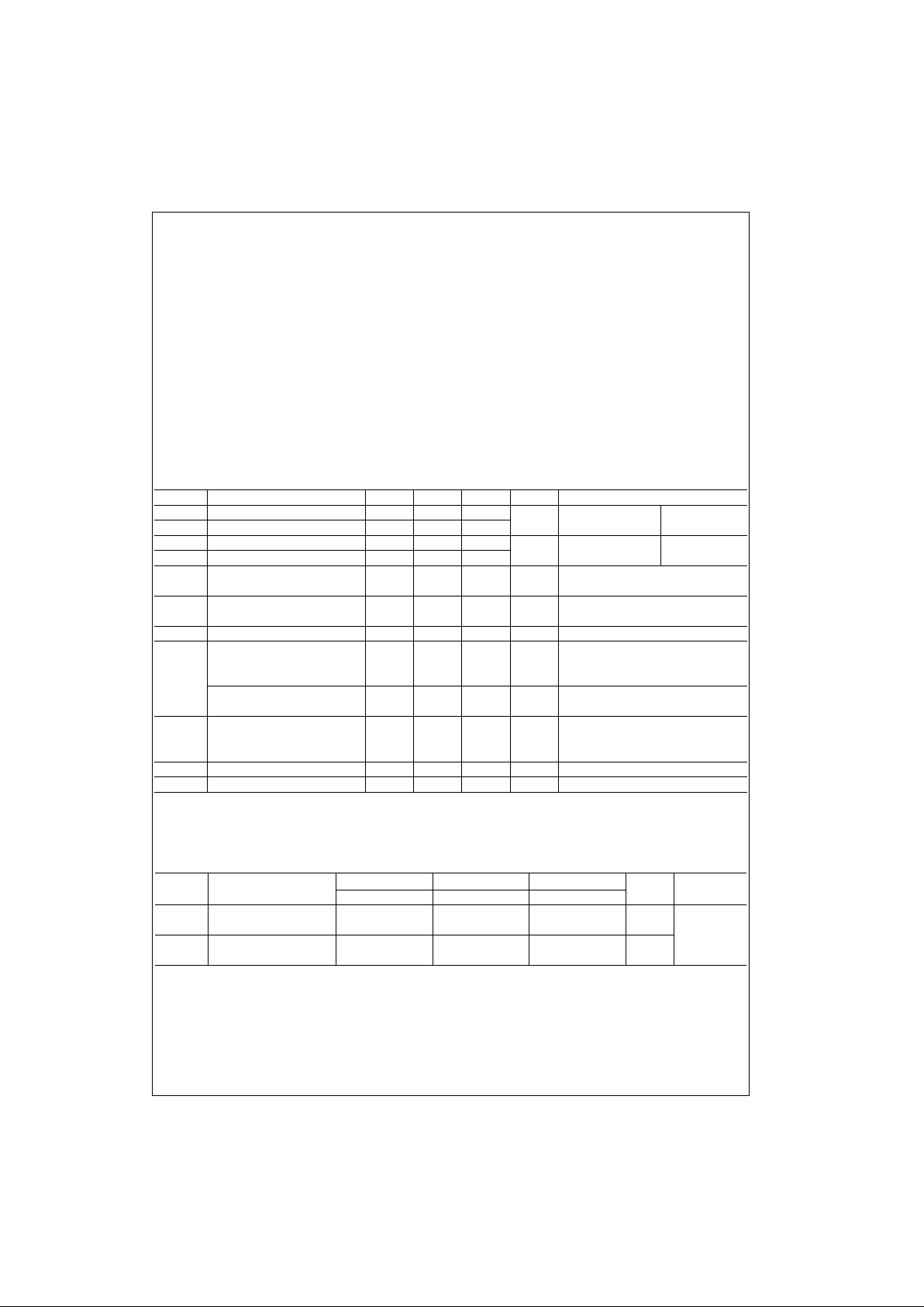
DC Electrical Characteristics
(Note 3)
V
EE
= −4.2V to −5.7V, VCC = V
CCA
= GND, TC = 0°C to +85°C, V
TTL
= +4.5V to +5.5V
Note 3: The specified limits represent the “worst case” value for the parameter. Since these values normally occur at the temperature extremes, additional
noise immunity and guardbanding can be achieved by decreasin g the al l owable syste m opera ti ng ran ge s. Cond it i ons fo r t estin g sho w n in the tabl es are chosen to guarantee operation under “worst case” conditions.
DIP AC Electric Characteristics
V
EE
= −4.2V to −5.7V, VCC = V
CCA
= GND, V
TTL
= +4.5V to +5.5V
Storage Temperature (T
STG
) −65°C to +150°C
Maximum Junction Temperature (T
J
) +150°C
V
EE
Pin Potential to Ground Pin −7.0V to +0.5V
V
TTL
Pin Potential to Ground Pin −0.5V to +6.0V
Input Voltage (DC)
−0.5V to +6.0V
Output Current (DC Output HIGH)
−50 mA
ESD (Note 2)
≥2000V
Case Temperature (T
C
)
Commercial 0
°C to +85°C
Industrial
−40°C to +85°C
Supply Voltage (V
EE
) −5.7V to −4.2V
Symbol Parameter Min Typ Max Units Conditions
V
OH
Output HIGH Voltage −1025 −955 −870
mV
VIN =V
IH (Max)
Loading with
V
OL
Output LOW Voltage −1830 −1705 −1620 or V
IL (Min)
50Ω to −2.0V
V
OHC
Output HIGH Voltage −1035
mV
VIN = V
IH(Min)
Loading with
V
OLC
Output LOW Voltage −1610 or V
IL (Max)
50Ω to −2.0V
V
IH
Input HIGH Voltage 2.0 5.0 V Guaranteed HIGH
Signal for All Inputs
V
IL
Input LOW Voltage 0 0.8 V Guaranteed LOW
Signal for All Inputs
V
CD
Input Clamp Diode Voltage −1.2 V IIN = −18 mA
I
IH
Input HIGH Current VIN = +2.4V,
Data 20 µA All Other Inputs V
IN
= GND
Enable 120
Input HIGH Current
1.0 mA
V
IN
= +5.5V,
Breakdown Test, All Inputs All Other Inputs = GND
I
IL
Input LOW Current VIN = +0.4V,
Data −0.9 mA All Other Inputs V
IN
= V
IH
Enable −5.4
I
EE
VEE Power Supply Current −70 −45 −22 mA All Inputs VIN = +4.0V
I
TTL
V
TTL
Power Supply Current 25 38 mA All Inputs VIN = GND
Symbol Parameter
T
C
= 0°CT
C
= +25°CT
C
= +85°C
Units Conditions
MinMaxMinMaxMinMax
t
PLH
Propagation Delay
0.50 3.00 0.50 2.90 0.50 3.00 ns
t
PHL
Data and Enable to Output Figures 2, 1
t
TLH
Transition Time
0.45 1.80 0.45 1.80 0.45 1.80 ns
t
THL
20% to 80%, 80% to 20%
Page 4

www.fairchildsemi.com 4
100324
Commercial Version (Continued)
SOIC and PLCC AC Electrical Characteristics
V
EE
= −4.2V to −5.7V, VCC = V
CCA
= GND, V
TTL
= +4.5V to +5.5V
Note 4: Output-to-Output Skew is defined as the absolute value of the difference between the actual propagation delay for any outputs within the same packaged device. Th e specif ications apply to any out puts s witchin g in the sa me dire ction e ither HI GH-to-LO W ( t
OSHL
), or LOW-to-HIGH ( t
OSLH
), or in opposite
directions both HL and LH (t
OST
). Parameters t
OST
and tPS guaranteed by design.
Symbol Parameter
TC = 0°CT
C
= +25°CT
C
= +85°C
Units Conditions
Min Max Min Max Min Max
t
PLH
Propagation Delay
0.50 2.80 0.50 2.70 0.50 2.80 ns
t
PHL
Data and Enable to Output Figures 2, 1
t
TLH
Transition Time
0.45 1.70 0.45 1.70 0.45 1.70 ns
t
THL
20% to 80%, 80% to 20%
t
OSHL
Maximum Skew Common Edge PLCC Only
Output-to-Output Variation 0.95 0.95 0.95 ns (Note 4)
Data to Output Path
t
OSLH
Maximum Skew Common Edge PLCC Only
Output-to-Output Variation 0.70 0.70 0.70 ns (Note 4)
Data to Output Path
t
OST
Maximum Skew Opposite Edge PLCC Only
Output-to-Output Variation 1.60 1.60 1.60 ns (Note 4)
Data to Output Path
t
PS
Maximum Skew PLCC Only
Pin (Signal) Transition Variation 1.20 1.20 1.20 ns (Note 4)
Data to Output Path
Page 5

5 www.fairchildsemi.com
100324
Industrial Version
DC Electrical Characteristics
(Note 5)
V
EE
= −4.2V to −5.7V, VCC = V
CCA
= GND, TC = −40°C to +85°C, V
TTL
= +4.5V to +5.5V
Note 5: The specified limits represent the “worst case” value for the parameter. Since these values normally occur at the temperature extremes, additional
noise immunity and guardbanding can be achieved by decreasin g the al l owable syste m opera ti ng ran ge s. Cond it i ons fo r t estin g sho w n in the tabl es are chosen to guarantee operation under “worst case” conditions.
AC Electrical Characteristics
V
EE
= −4.2V to −5.7V, VCC = V
CCA
= GND, V
TTL
= +4.5V to +5.5V
Symbol Parameter
T
C
= −40°CT
C
= 0°C to +85°C
Units Conditions
Min Max Min Max
V
OH
Output HIGH Voltage −1085 −870 −1025 −870
mV
VIN =V
IH (Max)
Loading with
V
OL
Output LOW Voltage −1830 −1575 −1830 −1620 or V
IL (Min)
50Ω to −2.0V
V
OHC
Output HIGH Voltage −1095 −1035
mV
VIN = V
IH(Min)
Loading with
V
OLC
Output LOW Voltage −1565 −1610 or V
IL (Max)
50Ω to −2.0V
V
IH
Input HIGH Voltage 2.0 5.0 2.0 5.0 V Guaranteed HIGH
Signal for All Inputs
V
IL
Input LOW Voltage 0 0.8 0 0.8 V Guaranteed LOW
Signal for All Inputs
V
CD
Input Clamp Diode Voltage −1.2 −1.2 V IIN = −18 mA
I
IH
Input HIGH Current VIN = +2.4V,
Data 20 20 µA All Other Inputs VIN = GND
Enable 120 120
Input HIGH Current
1.0 1.0 mA
VIN = +5.5V,
Breakdown Test, All Inputs All Other Inputs = GND
I
IL
Input LOW Current VIN = +0.4V,
Data −0.9 −0.9 mA All Other Inputs VIN = V
IH
Enable −5.4 −5.4
I
EE
VEE Power Supply Current −70 −22 −70 −22 mA All Inputs VIN = +4.0V
I
TTL
V
TTL
Power Supply Current 38 38 mA All Inputs VIN = GND
Symbol Parameter
T
C
= −40°CT
C
= +25°CT
C
= +85°C
Units Conditions
Min Max Min Max Min Max
t
PLH
Propagation Delay
0.50 2.80 0.50 2.70 0.50 2.80 ns Figures 2, 1
t
PHL
Data and Enable to Output
t
TLH
Transition Times
0.35 1.80 0.45 1.70 0.45 1.70 ns Figures 2, 1
t
THL
20% to 80%, 80% to 20%
Page 6

www.fairchildsemi.com 6
100324
Test Circuit
Note:
• V
CC
, V
CCA
= 0V, VEE = −4.5V, V
TTL
= +5.0V, VIH = +3.0V
• L1, L2 and L3 = equal length 50Ω impedance lines
• R
T
= 50Ω terminator internal to scope
• Decoupling 0.1 µF from GND to V
CC
, VEE and V
TTL
• All unused outputs are loaded with 50Ω to −2V or with equivalent E C L t erm inator network
• C
L
= Fixture and stray capacitance ≤ 3 pF
FIGURE 1. AC Test Circuit
Switching Waveform
FIGURE 2. Propagation Delay and Transition Times
Page 7

7 www.fairchildsemi.com
100324
Physical Dimensions inches (millimeters) unless otherwise noted
28-Lead Small Outline Integrated Circuit (SOIC), JEDEC MS-013, 0.300 Wide
Package Number M24B
24-Lead Plastic Dual-In-Line Package (PDIP), JEDEC MS-010, 0.400 Wide
Package Number N24E
Page 8

www.fairchildsemi.com 8
100324 Low Power Hex TTL-to-ECL Translator
Physical Dimensions inches (millimeters) unless otherwise noted (Continued)
28-Lead Plastic Lead Chip Carrier (PLCC), JEDEC MO-047, 0.450 Square)
Package Number V28A
Fairchild does not assume any responsibility for use of any circuitr y described, no circuit patent licenses are implied and
Fairchild reserves the right at any time without notice to change said circuitry and specifications.
LIFE SUPPORT POLICY
FAIRCHILD’S PRODUCTS ARE NOT AUTHORIZED FOR USE AS CRITICAL COMPONENTS IN LIFE SUPPORT
DEVICES OR SYSTEMS WITHOUT THE EXPRESS WRITTEN APPROVAL OF THE PRESIDENT OF FAIRCHILD
SEMICONDUCTOR CORPORATION. As used herein:
1. Life support devices or systems are devices or syste ms
which, (a) are intended for surgical implant into the
body, or (b) support or sustain life, and (c) whose failure
to perform when properly used in accordance with
instructions for use provided in the labeling, can be reasonably expected to result in a significant inju ry to the
user.
2. A critical component in any compon ent of a lif e supp ort
device or system whose failure t o perform can be reasonably expected to ca use the failure of the life supp ort
device or system, or to affect its safety or effectiveness.
www.fairchildsemi.com
 Loading...