

Page 1

© 2000 Fairchild Semiconductor Corporation DS009877 www.fairchildsemi.com
July 1988
Revised August 2000
100323 Low Power Hex Bus Driver
100323
Low Power Hex Bus Driver
General Description
The 100323 is a mo nolithic d evice contain ing six bu s drivers capable of driving ter min ate d li nes wit h ter min ati on s as
low as 25
Ω. To reduce crosstalk, each output has its own
respective ground connection. Transition times were
designed to be longer than on other F100K d evices. The
driver itself performs the pos itive log ic AND of a dat a input
(D
1–D6
) and the OR of two select inputs (E and either DE1,
DE
2
, or DE3).
Enabling of data is possi ble in mu ltiples of two , i.e. , 2, 4 or
all 6 paths. All inputs have 50 k
Ω pull-down resistors.
The output voltage LOW level is design ed to be more ne gative than normal ECL output s (cut off state). This allows
an emitter-follower output tra nsistor to turn OFF when the
termination supply is
−2.0V and thus present a high imped-
ance to the data bus.
Features
■ 50% power reduction of the 100123
■ 2000V ESD protection
■
−4.2V to −5.7V operating range
■ Drives 25
Ω load
Ordering Code:
Devices also availab le in Tape and Reel. Specify by appending th e s uffix let t er “X” to the ordering code.
Logic Symbol
Pin Descriptions
Connection Diagrams
24-Pin DIP
28-Pin PLCC
Order Number Package Number Package Description
100323PC N24E 24-Lead Plastic Dual-In-Line Package (PDIP), JEDEC MS-010, 0.400 Wide
100323QC V28A 28-Lead Plastic Lead Chip Carrier (PLCC), JEDEC MO-047, 0.450 Square
Pin Names Description
D
1–D6
Data Inputs
DE
1
–DE
3
Dual Enable Inputs
E Common Enable Input
O
1–O6
Data Outputs
Page 2
www.fairchildsemi.com 2
100323
Truth Table
H = HIGH Voltage Level
L = LOW Voltage Level
X = Don’t Care
Cutoff = Lower-than-LOW State
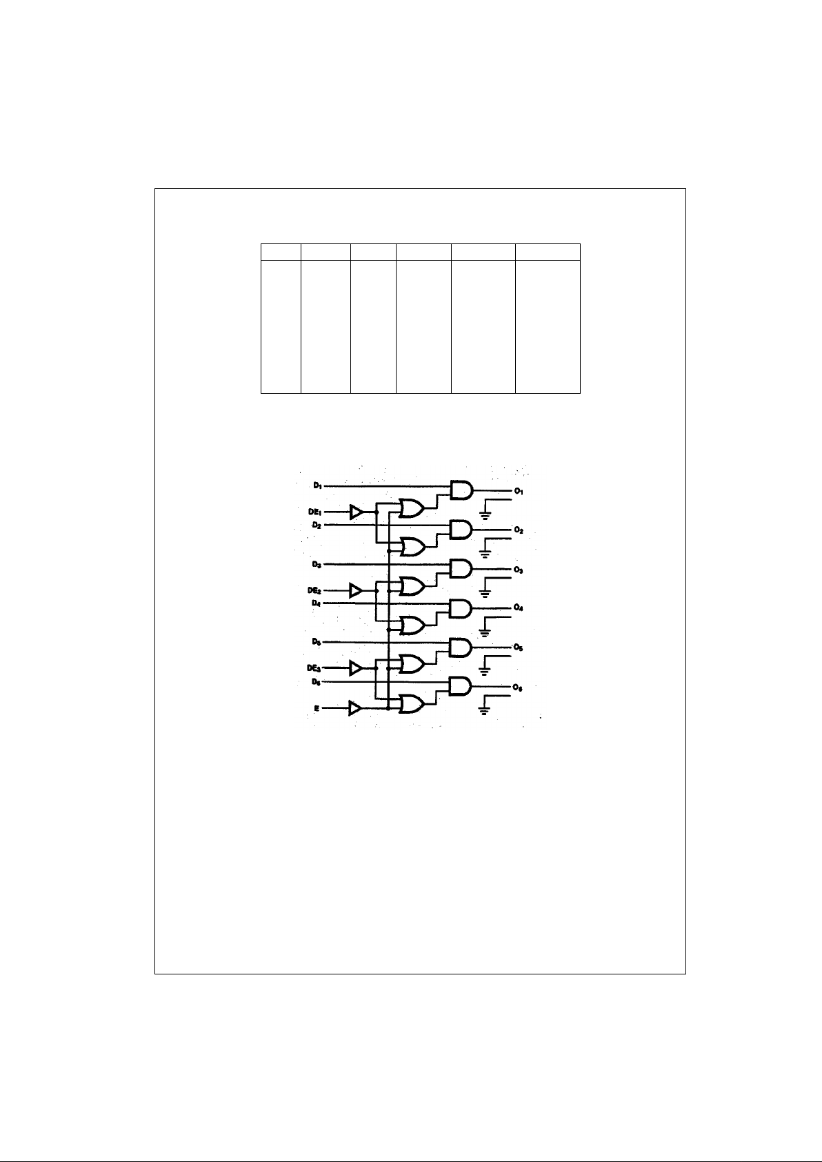
Logic Diagram
EDEnD
n
D
n+1
O
n
O
n+1
L L X X Cutoff Cutoff
X H L L Cutoff Cutoff
XH L H Cutoff H
X H H L H Cutoff
XH H H H H
H X L L Cutoff Cutoff
HX L H Cutoff H
H X H L H Cutoff
HX H H H H
Page 3

3 www.fairchildsemi.com
100323
Absolute Maximum Ratings(Note 1) Recommended Operating
Conditions
Note 1: The “Absolute Maximum Ratings” are those value s beyond which
the safety of the dev ice cannot b e guaranteed . The device sh ould not be
operated at these limit s. The parametric values defi ned in the Electrical
Characteristics tables are not guaranteed at the absolute maximum rating.
The “Recomm ended O peratin g Cond itions ” table will defin e the condition s
for actual device operation.
Note 2: ESD testing conforms to MIL-STD-883, Method 3015.
DC Electrical Characteristics (Note 3)
V
EE
= −4.2V to −5.7V, VCC = V
CCA
= GND, T
C
= 0°C to +85°C
Note 3: The specified limits represent “worst case” values for the parameter. Since these values normally occur at the temperature extremes, additional
noise immunity and guardbanding can be achieved by decreasin g the al l owable syste m opera ti ng ran ge s. Cond it i ons fo r t estin g sho w n in the tabl es are chosen to guarantee operation under “worst case” conditions.
DIP AC Electrical Characteristics (Note 4)
V
EE
= −4.2V to −5.7V, VCC = V
CCA
= GND
Note 4: The specified limits represent the “worst case” value for the parameter. Since these values normally occur at the temperature extremes, additional
noise immunity and guard banding ca n be a chie ve d by decr easi ng the allowable system operating ranges. Conditions for testing shown in the tables are chosen to guarantee operation under “worst case” conditions.
PLCC AC Electrical Characteristics (Note 5)
V
EE
= −4.2V to −5.7V, VCC = V
CCA
= GND
Note 5: The specified limits represent the “worst case” value for the parameter. Since these values normally occur at the temperature extremes, additional
noise immunity and guard banding ca n be a chie ve d by decr easi ng the allowable system operating ranges. Conditions for testing shown in the tables are chosen to guarantee operation under “worst case” conditions.
Storage Temperature −65°C to +150°C
Maximum Junction T emperature
+150°C
V
EE
Pin Potential to Ground Pin −7.0V to +0.5V
Input Voltage (DC) V
EE
to +0.5V
Output Current (DC Output High)
−50 mA
ESD
≥2000V
Case Temperature 0
°C to +85°C
Supply Voltage (V
EE
) −5.7V to −4.2V
Symbol Parameter Min Typ Max Units Conditions
V
IH
Input HIGH Voltage −1165 −870 mV Guaranteed High Signal for ALL Inputs
V
IL
Input LOW Voltage −1830 −1475 mV Guaranteed Low Signal for ALL Inputs
V
OH
Output HIGH Voltage −1025 −955 −870 mV VIN = V
IH (max)
or V
IL (min)
Loading with 25Ω to −2.0V
V
OHC
Output HIGH Voltage −1035 mV VIN = V
IH (min)
or V
IL (max)
Loading with 25Ω to −2.0V
V
OLZ
Cut-Off LOW Voltage −1950 mV VIN = V
IH (min)
or V
IL (max)
Loading with 25Ω to −2.0V
I
IL
Input LOW Current 0.50 µAVIN = V
IL (min)
I
IH
Input HIGH Current 240 µAVIN = V
IH (max)
I
EE
Power Supply Current −121 −91 −57 mA Inputs Open
Symbol Parameter
TC = 0°CT
C
= +25°CT
C
= +85°C
Units Conditions
Min Max Min Max Min Max
t
PZH
Propagation Delay 1.90 3.60 1.90 3.60 2.00 3.80
ns
Figures 1, 2
t
PHZ
Data to Output 1.30 2.70 1.30 2.70 1.50 2.70
t
PZH
Propagation Delay 1.90 3.60 1.90 3.60 2.00 3.90
ns
t
PHZ
Dual Enable to Output 1.60 3.00 1.60 3.00 1.70 3.40
t
PZH
Propagation Delay 1.80 3.50 1.80 3.50 2.00 3.80
ns
t
PHZ
Common Enable to Output 1.50 2.90 1.50 2.90 1.60 3.00
t
TZH
Transition Time 0.50 1.80 0.50 1.80 0.50 1.80
ns
t
THZ
20% to 80%, 80% to 20% 0.35 1.40 0.35 1.40 0.35 1.40
Symbol Parameter
TC = 0°CT
C
= +25°CT
C
= +85°C
Units Conditions
Min Max Min Max Min Max
t
PZH
Propagation Delay 1.90 3.40 1.90 3.40 2.00 3.60
ns
Figures 1, 2
t
PHZ
Data to Output 1.30 2.50 1.30 2.50 1.50 2.70
t
PZH
Propagation Delay 1.90 3.40 1.90 3.40 2.00 3.70
ns
t
PHZ
Dual Enable to Output 1.60 2.80 1.60 2.80 1.70 3.00
t
PZH
Propagation Delay 1.80 3.30 1.80 3.30 2.00 3.60
ns
t
PHZ
Common Enable to Output 1.50 2.70 1.50 2.70 1.60 2.80
t
TZH
Transition Time 0.50 1.70 0.50 1.70 0.50 1.70
ns
t
THZ
20% to 80%, 80% to 20% 0.35 1.30 0.35 1.20 0.35 1.30
Page 4

www.fairchildsemi.com 4
100323
Test Circuitry
Note:
• V
CC
, V
CCA
= +2V, VEE = −2.5V
• L1 and L2 = equal length 50Ω impedance lines
• R
T
= 50Ω terminator internal to scope
• Decoupling 0.1 µF from GND to V
CC
and V
EE
• All unused outputs are loaded with 25Ω to GND
• C
L
= Fixture and stray capacitance ≤ 3 pF
• Pin numbers show n are for flatpak; for DIP se e logic symbol
FIGURE 1. AC Test Circuit
Timing Waveform
FIGURE 2. Propagation Delay and Transition Times
Page 5

5 www.fairchildsemi.com
100323
Physical Dimensions inches (millimeters) unless otherwise noted
24-Lead Plastic Dual-In-Line Package (PDIP), JEDEC MS-010, 0.400 Wide
Package Number N24E
Page 6

www.fairchildsemi.com 6
100323 Low Power Hex Bus Driver
Physical Dimensions inches (millimeters) unless otherwise noted (Continued)
28-Lead Plastic Lead Chip Carrier (PLCC), JEDEC MO-047, 0.450 Square
Package Number V28A
Fairchild does not assume any responsibility for use of any circuitr y described, no circuit patent licenses are implied and
Fairchild reserves the right at any time without notice to change said circuitry and specifications.
LIFE SUPPORT POLICY
FAIRCHILD’S PRODUCTS ARE NOT AUTHORIZED FOR USE AS CRITICAL COMPONENTS IN LIFE SUPPORT
DEVICES OR SYSTEMS WITHOUT THE EXPRESS WRITTEN APPROVAL OF THE PRESIDENT OF FAIRCHILD
SEMICONDUCTOR CORPORATION. As used herein:
1. Life suppor t de vices o r systems a re devices or syste ms
which, (a) are intended for surgical implant into the
body, or (b) support or sustain life, and (c) whose failure
to perform when properly used in accordance with
instructions for use provided in the labeling, can be reasonably expected to result in a significant inju ry to the
user.
2. A critical compon ent i n any compon ent of a lif e support
device or system whose failure t o perform can be reasonably expected to ca use the failure of the life supp ort
device or system, or to affect its safety or effectiveness.
www.fairchildsemi.com
 Loading...