

Page 1
© 1999 Fairchild Semiconductor Corporation DS010943 www.fairchildsemi.com
October 1991
Revised November 1999
100310 Low Skew 2:8 Differential Clock Driver
100310
Low Skew 2:8 Differential Clock Driver
General Description
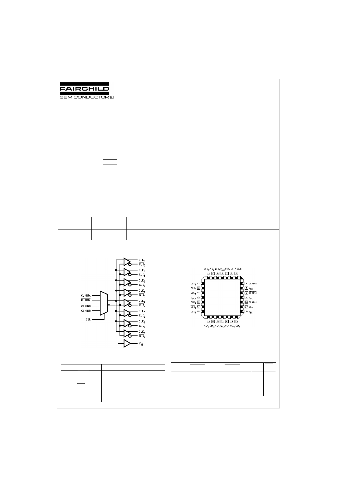
The 100310 is a low skew 8-bit differential clock driver
which is designed to select between two sep arate differe ntial clock inputs. The lo w ou tpu t to ou tput skew (< 50 ps) is
maintained for either clock input. A LOW on the sele ct pin
(SEL) selects CLKINA, CLKINA
and a HIGH on th e SEL
pin selects the CLKINB, CLKINB
inputs.
The 100310 is ideal for tho se applications that need the
ability to freely select between two clocks, or to maintain
the ability to switch to an alternate or backup clock should a
problem arise with the primary clock source.
A V
BB
output is provided for single-ended operation.
Features
■ Low output to output skew
■ Differential inputs and outputs
■ Allows multiplexing between two clock inputs
■ Voltage compensated operating range: −4.2V to −5.7V
■ Available to industrial grade temperature range
(PLCC package only)
Ordering Code:
Devices also availab le in Tape and Reel. Specify by appending th e s uffix let t er “X” to the ordering code.
Logic Symbol
Pin Descriptions
Connection Diagram
28-Pin PLCC
Truth T able
Order Number Package Number Package Description
100310QC V28A 28-Lead Plastic Lead Chip Carrier (PLCC), JEDEC MO-047, 0.450 Square
100310QI V28A 28-Lead Plastic Lead Chip Carrier (PLCC), JEDEC MO-047, 0.450 Square
Industrial Temperature Range (−40°C to +85°C)
Pin Names Description
CLKIN
n
, CLKIN
n
Differential Clock Inputs
SEL Select
CLK
0–7
, CLK
0–8
Differential Clock Outputs
V
BB
VBB Output
NC No Connect
CLKINA CLKINA CLKINB CLKINB SEL
CLK
n
CLK
n
HLXXLHL
LHXXLLH
XXHLHHL
XXLHHLH
Page 2
www.fairchildsemi.com 2
100310
Absolute Maximum Ratings(Note 1) Recommended Operating
Conditions
Note 1: The “Absolute Maximum Ratings” are those values beyon d which
the safety of the dev ice cannot be guaranteed. T he device sh ould not be
operated at these limit s. The parametric values defin ed in the Electrical
Characteristics tables are not guaranteed at the absolute maximum rating.
The “Recomme nded O peratin g Cond itions ” table will defin e the condition s
for actual device operation.
Note 2: ESD testing conf orm s t o M I L-STD-883, Method 3015.
Commercial Version
DC Electrical Characteristics
(Note 3)
V
EE
= −4.2V to −5.7V, VCC = V
CCA
= GND, TC = 0°C to +85°C
Note 3: The specified limits represent the “worst case” value for the parameter. Since these values normally occur at the temperature extremes, additional
noise immunity and guardbanding can be achieved by decreasing the all owable syste m opera ti ng r ange s. Co ndi ti ons fo r t est ing shown in the ta ble s are chosen to guarantee operation under “worst case” conditions.
Storage Temperature (T
STG
) −65°C to +150°C
Maximum Junction Temperature (T
J
) +150°C
Pin Potential to Ground Pin (V
EE
) −7.0V to +0.5V
Input Voltage ( DC) V
EE
to +0.5V
Output Current (DC Output HIGH) −50 mA
ESD (Note 2) ≥2000V
Case Temperature (T
C
)
Commercial 0°C to +85°C
Industrial −40°C to +85°C
Supply Voltage ( V
EE
) −5.7V to −4.2V
Symbol Parameter Min Typ Max Units Conditions
V
OH
Output HIGH Voltage −1025 −955 −870 mV VIN = VIH (Max) Loading with
V
OL
Output LOW Voltage −1830 −1705 −1620 mV or VIL (Min) 50Ω to −2.0V
V
OHC
Output HIGH Voltage −1035 mV VIN = VIH Loading with
V
OLC
Output LOW Voltage −1610 mV or VIL (Max) 50Ω to −2.0V
V
BB
Output Reference Voltage −1380 −1320 −1260 mV I
VBB
= −250 µA
V
DIFF
Input Voltage Differential 150 mV Required for Full Output Swing
V
CM
Common Mode Voltage VCC − 2.0 VCC − 0.5 V
V
IH
Input HIGH Voltage −1165 −870 mV Guaranteed HIGH Signal for All Inputs
V
IL
Input LOW Voltage −1830 −1475 mV Guaranteed LOW Signal for All Inputs
I
IL
Input LOW Current 0.50 µAVIN = VIL (Min)
I
IH
Input HIGH Current 240 µAVIN = VIH (Max)
I
CBO
Input Leakage Current −10 µAVIN = V
EE
I
EE
Power Supply Current −100 −40 mA Inputs Open
Page 3

3 www.fairchildsemi.com
100310
Commercial Version (Continued)
AC Electrical Characteristics
VEE = −4.2V to −5.7V, VCC = V
CCA
= GND
Note 4: tPS describes opposite edge skews, i.e. the differen ce between the delay of a differential output signal pa ir’s LO W-to-HIGH and HIGH-to-LOW prop-
agation delays. With differential signal pairs, a LO W-to-HIGH or HIGH-to- LOW transition is defined as th e t ransition of the true output or input pin.
Note 5: t
OSLH
describes in-phase ga t e-to-gate different i al propagat ion skews wi t h all dif f erential ou t puts going LO W -to-HIGH; t
OSHL
describes the same conditions except with th e outputs going HIGH-to-LOW.
Note 6: t
OST
describes the max im um worst case difference in any of the tPS, t
OSLH
or t
OST
delay paths combined.
Note 7: The skew specifications pertain to differential I/O pat hs .
Symbol Parameter
T
C
= 0°CT
C
= +25°CT
C
= +85°C
Units Conditions
Min Typ Max Min Typ Max Min Typ Max
f
MAX
Max Toggle Frequency
CLKIN A/B to Qn750 750 750 MHz
SEL to Q
n
575 575 575 MHz
t
PLH
Propagation Delay,
t
PHL
CLKINn to CLK
n
Differential 0.80 0.90 1.00 0.82 0 .92 1 .02 0 .89 1.01 1.09 ns Figure 3
Single-Ended 0.80 0.96 1.20 0.82 0.98 1.22 0.89 1.06 1.29
t
PLH
Propagation Delay,
0.75 0.99 1.20 0.80 1.02 1.25 0.85 1.10 1.35 ns Figure 2
t
PHL
SEL to Output
t
PS
LH-HL Skew 10 30 10 30 10 30
ps
(Note 4)(Note 7)
t
OSLH
Gate-Gate Skew LH 20 30 20 50 20 50 (Note 5)(Note 7)
t
OSHL
Gate-Gate Skew HL 20 50 20 50 20 50 (Note 5)(Note 7)
t
OST
Gate-Gate LH-HL Skew 30 60 30 60 30 60 (Note 6)(Note 7)
t
S
Setup Time
300 300 300 ps
SEL to CLKIN
n
t
H
Setup Time
000ps
SEL to CLKIN
n
t
TLH
Transition Time
275 510 750 275 500 750 275 480 750 ps Figure 4
t
THL
20% to 80%, 80% to 20%
Page 4

www.fairchildsemi.com 4
100310
Industrial Version
DC Electrical Characteristics
(Note 8)
V
EE
= −4.2V to −5.7V, VCC = V
CCA
= GND
Note 8: The specified limits represent the “worst case” value for the parameter. Since these values normally occur at the temperature extremes, additional
noise immunity and guardbanding can be achieved by decreasing the all owable syste m opera ti ng r ange s. Co ndi ti ons fo r t est ing shown in the ta ble s are chosen to guarantee operation under “worst case” conditions.
AC Electrical Characteristics
VEE = −4.2V to −5.7V, VCC = V
CCA
= GND
Note 9: tPS describes opposite edge skews, i.e. the difference between the delay of a differential output signal pa ir' s LOW -t o-HIGH and HIGH-to-LOW prop-
agation delays. With differential signal pairs, a LOW-to-HIGH or HIGH-to-LOW transition is defined as the transition of the true outp ut or input pin.
Note 10: t
OSLH
describes in-phas e gate-to-g ate different ial propaga tion skew s with all d ifferential ou tputs goin g LOW-to-HIG H; t
OSHL
describes the same
conditions except with the outputs going HIGH-to-LOW.
Note 11: t
OST
describes the maxi m um w orst case difference in any of the tPS, t
OSLH
or t
OST
delay paths combined.
Note 12: The skew specifications pertain to differential I/O paths.
Symbol Parameter
T
C
= −40°CTC = 0°C to +85°C
Units Conditions
Min Max Min Max
V
OH
Output HIGH Voltage −1085 −870 −1025 −870 mV VIN = VIH (Max) Loading with
V
OL
Output LOW Voltage −1830 −1575 −1830 −1620 mV or VIL (Min) 50Ω to −2.0V
V
OHC
Output HIGH Voltage −1095 −1035 mV VIN = V
IH
Loading with
V
OLC
Output LOW Voltage −1565 −1610 mV or VIL (Min) 50Ω to −2.0V
V
BB
Output Reference Voltage −1395 −1255 −1380 −1260 mV I
VBB
= −250 µA
V
DIFF
Input Voltage Differential 150 150 mV Required for Full Output Swing
V
CM
Common Mode Voltage VCC − 2.0 VCC − 0.5 VCC − 2.0 VCC − 0.5 V
V
IH
Input HIGH Voltage −1170 −870 −1165 −870 mV Guaranteed HIGH Signal for
All Inputs
V
IL
Input LOW Voltage −1830 −1480 −1830 −1475 mV Guaranteed LOW Signal for
All Inputs
I
IL
Input LOW Current 0.50 0.50 µAVIN = VIL (Min)
I
IH
Input HIGH Current 240 240 µAVIN = VIH (Max)
I
CBO
Input Leakage Current −10 −10 µAVIN = V
EE
I
EE
Power Supply Current −100 −40 −100 −40 mA Inputs Open
Symbol Parameter
TC = −40°CT
C
= +25°CT
C
= +85°C
Units Conditions
Min Typ Max Min Typ Max Min Typ Max
f
MAX
Max T oggle Frequency
CLKIN A/B to Qn750 750 750 MHz
SEL to Q
n
575 575 575 MHz
t
PLH
Propagation Delay,
t
PHL
CLKINn, to CLK
n
Differential 0.78 0.88 0.98 0.82 0.92 1.02 0.89 1.01 1.09 ns Figure 3
Single-Ended 0.78 0.95 1.18 0.82 0.98 1.22 0.89 1.06 1.29
t
PLH
Propagation Delay
0.70 0.99 1.20 0.80 1.02 1.25 0.85 1.10 1.35 ns Figure 2
t
PHL
SEL to Output
t
PS
LH-HL Skew 10 30 10 30 10 30 (Note 9)(Note 12)
t
OSLH
Gate-Gate Skew LH 20 50 20 50 20 50 ps (Note 10)(Note 12)
t
OSHL
Gate-Gate Skew HL 20 50 20 50 20 50 (Note 10)(Note 12)
t
OST
Gate-Gate LH-HL Skew 30 60 30 60 30 60 (Note 11)(Note 12)
t
S
Setup Time
300 300 300 ps
SEL to CLKIN
n
t
H
Setup Time
000ps
SEL to CLKIN
n
t
TLH
Transition Time
275 510 750 275 500 750 275 480 750 ps Figure 4
t
THL
20% to 80%, 80% to 20%
Page 5

5 www.fairchildsemi.com
100310
Test Circuit
Note:
Shown for testing CLKIN to CLK1 in the differential mode.
L1, L2, L3 and L4 = equal length 50Ω impedance lines.
All unused inputs and outputs are loaded with 50Ω in parallel with ≤3 pF to GND.
Scope should have 50Ω input terminator internally.
FIGURE 1. AC Test Circuit
Switching Waveforms
FIGURE 2. Propagation Delay, SEL to Outputs
FIGURE 3. Propagation Delay, CLKIN/CLKIN
to Outputs
FIGURE 4. Transition Times
Page 6

www.fairchildsemi.com 6
100310 Low Skew 2:8 Differential Clock Driver
Physical Dimensions inches (millimeters) unless otherwise noted
28-Lead Plastic Lead Chip Carrier (PLCC), JEDEC MO-047, 0.450 Square
Package Number V28A
Fairchild does not assume any responsibility for use of any circuitr y described, no circuit patent licenses are implied and
Fairchild reserves the right at any time without notice to change said circuitry and specifications.
LIFE SUPPORT POLICY
FAIRCHILD’S PRODUCTS ARE NOT AUTHORIZED FOR USE AS CRITICAL COMPONENTS IN LIFE SUPPORT
DEVICES OR SYSTEMS WITHOUT THE EXPRESS WRITTEN APPROVAL OF THE PRESIDENT OF FAIRCHILD
SEMICONDUCTOR CORPORATION. As used herein:
1. Life support devices or systems are devices or systems
which, (a) are intended for surgical implant into the
body, or (b) support or sustain life, and (c) whose failure
to perform when properly used in accordance with
instructions for use provided in the labeling, can be reasonably expected to result in a significant inju ry to the
user.
2. A critical component in any compon ent of a l ife supp ort
device or system whose failure t o perform can be reasonably expected to ca use the failure of the life supp ort
device or system, or to affect its safety or effectiveness.
www.fairchildsemi.com
 Loading...