

Datasheet 100301SCX, 100301SC, 100301QIX, 100301QI, 100301QCX Datasheet (Fairchild Semiconductor)
...Page 1
© 2000 Fairchild Semiconductor Corporation DS010579 www.fairchildsemi.com
August 1989
Revised August 2000
100301 Low Power Tri ple 5-Input OR/NOR Gate
100301
Low Power Triple 5-Input OR/NOR Gate
General Description
The 100301 is a mono l ithic triple 5-input OR/NOR ga te. All
inputs have 50 k
Ω pull-down resistors and all outputs are
buffered.
Features
■ 23% power reduction of the 100101
■ 2000V ESD protection
■ Pin/function compatible with 100101
■ Voltage compensated operating range
= −4.2V to −5.7V
■ Available to industrial grade temperature range
(PLCC package only)
Ordering Code:
Devices also availab le in Tape and Reel. Specify by appending th e s uffix let t er “X” to the ordering code.
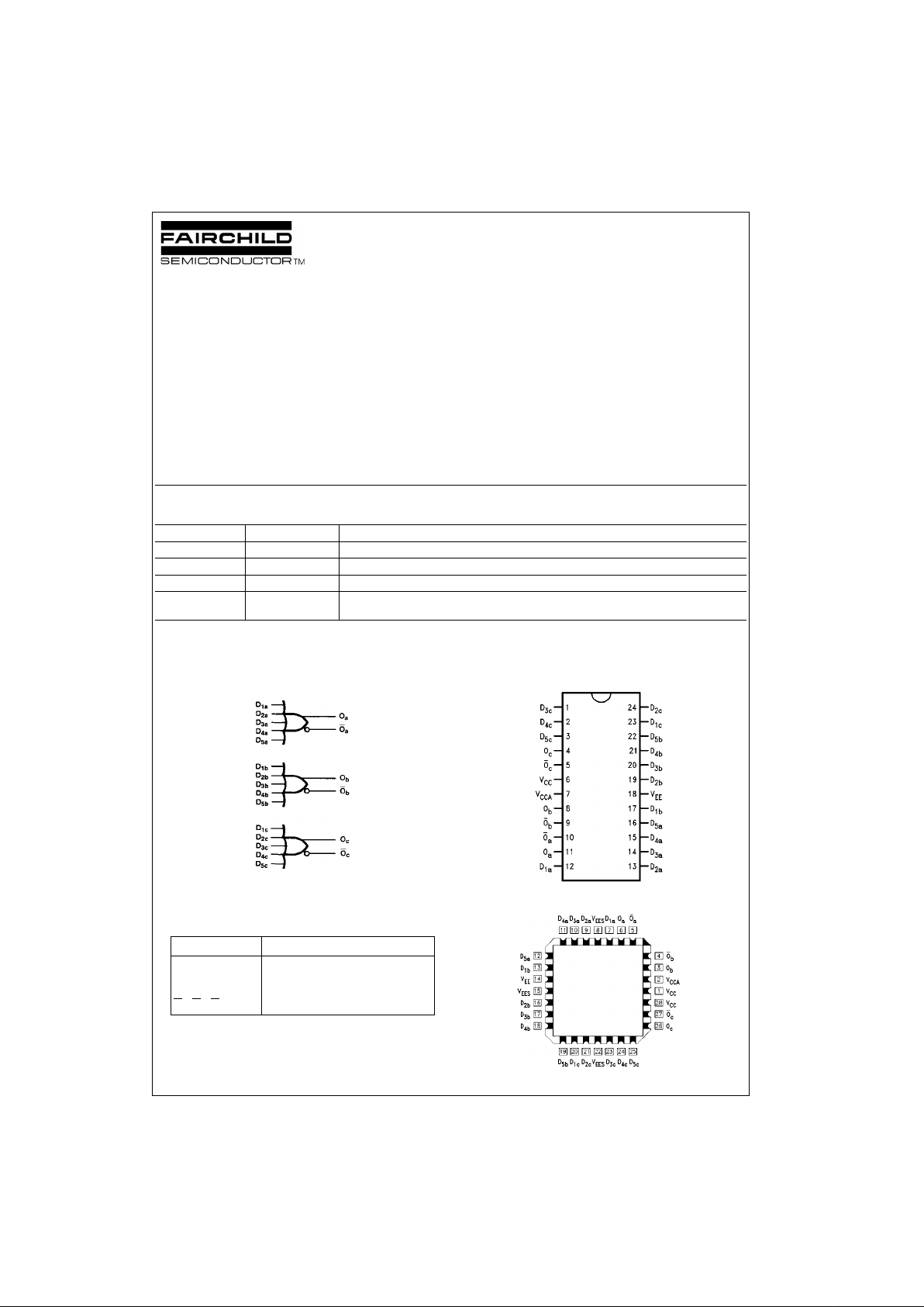
Logic Symbol
Pin Descriptions
Connection Diagrams
24-Pin DIP/SOIC
28-Pin PLCC
Order Number Package Number Package Description
100301SC M24B 24-Lead Small Outline Integrated Circuit (SOIC), JEDEC MS-013, 0.300 Wide
100301PC N24E 24-Lead Plastic Dual-In-Line Package (PDIP), JEDEC MS-010, 0.400 Wide
100301QC V28A 28-Lead Plastic Lead Chip Carrier (PLCC), JEDEC MO-047, 0.450 Square
100301QI V28A 28-Lead Plastic Lead Chip Carrier (PLCC), JEDEC MO-047, 0.450 Square
Industrial Temperature Range (
−40°C to +85°C)
Pin Names Description
D
na
, Dnb, D
nc
Data Inputs
O
a
, Ob, O
c
Data Outputs
O
a
, Ob, O
c
Complementary Data Output s
Page 2
www.fairchildsemi.com 2
100301
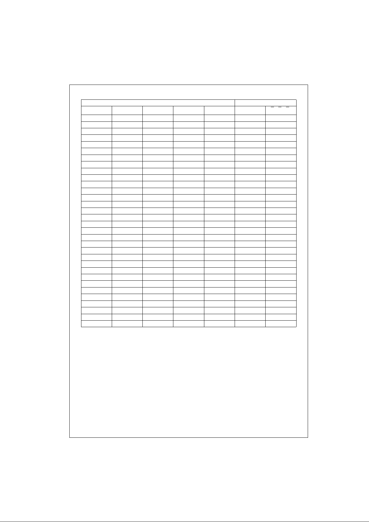
Truth Table
H = HIGH Voltage Level
L = LOW Voltage Level
Inputs Outputs
D
1a
, D1b, D1cD2a, D2b, D2cD3a, D3b, D3cD4a, D4b, D4cD5a, D5b, D5cOa, Ob, OcOa, Ob, O
c
LLLLLLH
LLLLHHL
LLLHLHL
LLLHHHL
LLHLLHL
LLHLHHL
LLHHLHL
LLHHHHL
LHLLLHL
LHLLHHL
LHLHLHL
LHLHHHL
LHHLLHL
LHHLHHL
LHHHLHL
LHHHHHL
HLLLLHL
HLLLHHL
HLLHLHL
HL LHHHL
HLHLLHL
HLHLHHL
HLHHLHL
HLHHHHL
HHLLLHL
HHL LHHL
HHLHLHL
HHLHHHL
HHHL LHL
HHHLHHL
HHHHLHL
HHHHHHL
Page 3
3 www.fairchildsemi.com
100301
Absolute Maximum Ratings(Note 1) Recommended Operating
Conditions
Note 1: The “Absolute Maximum Ratings” are those value s beyond which
the safety of the dev ice cannot b e guaranteed . The device sh ould not be
operated at these limit s. The parametric values defi ned in the Electrical
Characteristics tables are not guaranteed at the absolute maximum rating.
The “recommended Operating Conditions” table will define t he condition s
for actual device operation.
Note 2: ESD testing conforms to MIL-STD-883, Method 3015.
Commercial Version
DC Electrical Characteristics
(Note 3)
V
EE
= −4.2V to −5.7V, VCC = V
CCA
= GND, T
C
= 0°C to +85°C
Note 3: The specified limits represent the “worst case” value for the parameter. Since these values normally occur at the temperature extremes, additional
noise immunity and guardbanding can be achieved by decreasin g the al l owable syste m opera ti ng ran ge s. Cond it i ons fo r t estin g sho w n in the tabl es are chosen to guarantee operation under “worst case” conditions.
DIP AC Electrical Characteristics
V
EE
= −4.2V to −5.7V, VCC = V
CCA
= GND
Note 4: The propagation delay s pec ified is for single output swit c hing. Delays may vary up to 100 ps with multiple outpu ts s witching.
Storage Temperature (T
STG
) −65°C to +150°C
Maximum Junction Temperature (T
J
) +150°C
V
EE
Pin Potential to Ground Pin −7.0V to +0.5V
Input Voltage (DC) V
EE
to +0.5V
Output Current (DC Output HIGH)
−50 mA
ESD (Note 2)
≥2000V
Case Temperature (T
C
)
Commercial 0
°C to +85°C
Industrial
−40°C to +85°C
Supply Voltage (V
EE
) −5.7V to −4.2V
Symbol Parameter Min Typ Max Units Conditions
V
OH
Output HIGH Voltage −1025 −955 −870 mV
VIN = V
IH(Max)
or V
IL(Min)
Loading with
V
OL
Output LOW Voltage −1830 −1705 −1620 mV 50Ω to −2.0V
V
OHC
Output HIGH Voltage −1035 mV
VIN = V
IH(Min)
or V
IL(Max)
Loading with
V
OLC
Output LOW Voltage −1610 mV 50Ω to −2.0V
V
IH
Input HIGH Voltage −1165 −870 mV Guaranteed HIGH Signal for All Inputs
V
IL
Input LOW Voltage −1830 −1475 mV Guaranteed LOW Signal for All Inputs
I
IL
Input LOW Current 0.50 µAVIN = V
IL(Min)
I
IH
Input HIGH Current 240 µAVIN = V
IH(Max)
I
EE
Power Supply Current −29 −17 −15 mA Inputs OPEN
Symbol Parameter
TC = 0°CT
C
= +25°CT
C
= +85°C
Units Conditions
Min Max Min Max Min Max
t
PLH
Propagation Delay
0.50 1.10 0.50 1.15 0.50 1.20 ns
Figures 1, 2
t
PHL
Data to Output (Note 4)
t
TLH
Transition Time
0.40 1.20 0.40 1.20 0.40 1.20 ns Figures 1, 2
t
THL
20% to 80%, 80% to 20%
Page 4

www.fairchildsemi.com 4
100301
Commercial Version (Continued)
SOIC and PLCC AC Electrical Characteristics
V
EE
= −4.2V to −5.7V, VCC = V
CCA
= GND
Note 5: The propagation dela y sp ec if ied is for single output swit c hing. Delays may vary up to 100 ps with multiple outpu ts s w it c hing.
Note 6: Output-to-Output Skew is defined as the absolute value of the difference between the actual propagation delay for any outputs within the same pack-
aged device. Th e specif ications apply to any out puts s witchin g in the sa me dire ction e ither HI GH-to-LO W ( t
OSHL
), or LOW-to-HIGH ( t
OSLH
), or in opposite
directions both HL and LH (t
OST
). Parameters t
OST
and tPS guaranteed by design.
Industrial Version
PLCC DC Electrical Characteristics
(Note 7)
V
EE
= −4.2V to −5.7V, VCC = V
CCA
= GND, T
C
= −40°C to +85°C
Note 7: The specified limits represent the “worst case” value for the parameter. Since these values normally occur at the temperature extremes, additional
noise immunity and guardbanding can be achieved by decreasing the all owable syste m opera ti ng r ange s. Co ndi ti ons fo r t est ing shown in the ta ble s are chosen to guarantee operation under “worst case” conditions.
PLCC AC Electrical Characteristics
V
EE
= −4.2V to −5.7V, VCC = V
CCA
= GND
Note 8: The propagation dela y sp ec if ied is for single output swit c hing. Delays may vary up to 100 ps with multiple outpu ts s w it c hing.
Symbol Parameter
TC = 0°CT
C
= +25°CT
C
= +85°C
Units Conditions
Min Max Min Max Min Max
t
PLH
Propagation Delay
0.50 1.00 0.50 1.05 0.50 1.10 ns
Figures 1, 2
t
PHL
Data to Output (Note 5)
t
TLH
Transition Time
0.40 1.10 0.40 1.10 0.40 1.10 ns Figures 1, 2
t
THL
20% to 80%, 80% to 20%
t
OSHL
Maximum Skew Common Edge PLCC Only
Output-to-Output Variation 240 240 240 ps (Note 6)
Data to Output Path
t
OSLH
Maximum Skew Common Edge PLCC Only
Output-to-Output Variation 330 330 330 ps (Note 6)
Data to Output Path
t
OST
Maximum Skew Opposite Edge PLCC Only
Output-to-Output Variation 330 330 330 ps (Note 6)
Data to Output Path
t
PS
Maximum Skew PLCC Only
Pin (Signal) Transition Variation 230 230 230 ps (Note 6)
Data to Output Path
Symbol Parameter
TC = −40°CTC = 0°C to +85°C
Units Conditions
Min Max Min Max
V
OH
Output HIGH Voltage −1085 −870 −1025 −870 mV VIN = V
IH(Max)
Loading with
V
OL
Output LOW Voltage −1830 −1575 −1830 −1620 mV or V
IL(Min)
50Ω to −2.0V
V
OHC
Output HIGH Voltage −1095 −1035 mV VIN = V
IH(Min)
Loading with
V
OLC
Output LOW Voltage −1565 −1610 mV or V
IL(Max)
50Ω to −2.0V
V
IH
Input HIGH Voltage −1170 −870 −1165 −870 mV Guaranteed HIGH Signal for All Inputs
V
IL
Input LOW Voltage −1830 −1480 −1830 −1475 mV Guaranteed LOW Signal for All Inputs
I
IL
Input LOW Current 0.50 0.50 µAVIN = V
IL(Min)
I
IH
Input HIGH Current 240 240 µAVIN = V
IH(Max)
I
EE
Power Supply Current −29 −15 −29 −15 mA Inputs Open
Symbol Parameter
TC = −40°CT
C
= +25°CT
C
= +85°C
Units Conditions
Min Max Min Max Min Max
t
PLH
Propagation Delay
0.40 1.00 0.50 1.05 0.50 1.10 ns
Figures 1, 2
t
PHL
Data to Output (Note 8)
t
TLH
Transition Time
0.30 1.10 0.40 1.10 0.40 1.10 ns Figures 1, 2
t
THL
20% to 80%, 80% to 20%
Page 5

5 www.fairchildsemi.com
100301
Test Circuitry
Notes:
V
CC
, V
CCA
= +2V, VEE = −2.5V
L1 and L2 = equal length 50Ω impedanc e lines
R
T
= 50Ω terminator internal to scope
Decouplin g 0.1 µF from GND to V
CC
and V
EE
All unused outputs are loaded with 50Ω to GND
C
L
= Fixture and stray capacitance ≤ 3 pF
FIGURE 1. AC Test Circuit
Switching Waveforms
FIGURE 2. Propagation Delay and Transition Times
Page 6

www.fairchildsemi.com 6
100301
Physical Dimensions inches (millimeters) unless otherwise noted
24-Lead Small Outline Integrated Circuit (SOIC), JEDEC MS-013, 0.300 Wide
Package Number M24B
24-Lead Plastic Dual-In-Line Package (PDIP), JEDEC MS-010, 0.400 Wide
Package Number N24E
Page 7

7 www.fairchildsemi.com
100301 Low Power Tri ple 5-Input OR/NOR Gate
Physical Dimensions inches (millimeters) unless otherwise noted (Continued)
28-Lead Plastic Lead Chip Carrier (PLCC), JEDEC MO-047, 0.450 Square
Package Number V28A
Fairchild does not assume any responsibility for use of any circuitry described , no circuit patent licenses are implied and
Fairchild reserves the right at any time without notice to change said circuitry and specifications.
LIFE SUPPORT POLICY
FAIRCHILD’S PRODUCTS ARE NOT AUTHORIZED FOR USE AS CRITICAL COMPONENTS IN LIFE SUPPORT
DEVICES OR SYSTEMS WITHOUT THE EXPRESS WRITTEN APPROVAL OF THE PRESIDENT OF FAIRCHILD
SEMICONDUCTOR CORPORATION. As used herein:
1. Life support devices or systems are dev ic es or syste ms
which, (a) are intended for surgical implant into the
body, or (b) support or sustain life, and (c) whose failure
to perform when properly used in accordance with
instructions for use provide d in the labe l ing, can be re asonably expected to result in a significant injury to the
user.
2. A critical compo nent in any com ponen t of a life s upp ort
device or system whose failure to perform can be reasonably expected to cause the failure of the l ife support
device or system, or to affect its safety or effectiveness.
www.fairchildsemi.com
 Loading...