

data delay devices 3D7205 Service Manual

(
)
查询3D7205供应商
3D7205
MONOLITHIC 5-TAP
FIXED DELAY LINE
(SERIES 3D7205)
FEATURES PACKAGES
1
• All-silicon, low-power CMOS
technology
• TTL/CMOS compatible
O2
O4
GND
IN
inputs and outputs
• Vapor phase, IR and wave
solderable
• Auto-insertable (DIP pkg.)
• Low ground bounce noise
• Leading- and trailing-edge accuracy
• Delay range: 8 through 500ns
• Delay tolerance: 5% or 2ns
• Temperature stability: ±3% typical (0C-70C)
• Vdd stability: ±2% typical (4.75V-5.25V)
• Minimum input pulse width: 20% of total delay
• 14-pin DIP and 16-pin SOIC available as drop-in
replacements for hybrid delay lines
FUNCTIONAL DESCRIPTION
The 3D7205 5-Tap Delay Line product family consists of fixed-delay
CMOS integrated circuits. Each package contains a single delay line,
tapped and buffered at 5 points spaced uniformly in time. Tap-to-tap
(incremental) delay values can range from 8.0ns through 100ns. The
input is reproduced at the outputs without inversion, shifted in time as
per the user-specified dash number. The 3D7205 is TTL- and CMOScompatible, capable of driving ten 74LS-type loads, and features both
rising- and falling-edge accuracy.
The all-CMOS 3D7205 integrated circuit has been designed as a
reliable, economic alternative to hybrid TTL fixed delay lines. It is offered in a standard 8-pin autoinsertable DIP and a space saving surface mount 8-pin SOIC.
TABLE 1: PART NUMBER SPECIFICATIONS
DIP-8
3D7205M
3D7205H
-8 -8 -8 -8
-10 -10 -10 -10
-15 -15 -15 -15
-20 -20 -20 -20
-25 -25 -25 -25
-30 -30 -30 -30
-50 -50 -50 -50
-75 -75 -75 -75
-100 -100 -100 -100
PART NUMBER TOLERANCES INPUT RESTRICTIONS
SOIC-8
3D7205Z
DIP-14
3D7205
3D7205
G
3D7205K
SOIC-16
3D7205S
DELAY (ns)
250 ± 12.5 50.0 ± 5.0
375 ± 18.8 75.0 ± 7.5
500 ± 25.0 100 ± 10.0
8
VDD
2
7
3
6
4
5
O1
O3
O5
3D7205Z
SOIC
GND
(150 Mil)
GND
TOTAL
40.0 ± 2.0 8.0 ± 1.5
50.0 ± 2.5 10.0 ± 2.0
75.0 ± 3.8 15.0 ± 2.3
100 ± 5.0 20.0 ± 2.5
125 ± 6.3 25.0 ± 2.5
150 ± 7.5 30.0 ± 3.0
TAP-TAP
DELAY
(ns)
IN
O2
O4
1
2
3
4
VDD
8
O1
7
O3
6
O5
5
3D7205M DIP
3D7205H Gull-Wing
N/C
N/C
O2
N/C
O4
N/C
1
IN
2
3
4
5
6
7
8
VDD
16
N/C
15
N/C
14
O1
13
N/C
12
O3
11
N/C
10
O5
9
IN
1
N/C
N/C
O2
N/C
O4
GND
2
3
4
5
6
7
3D7205 DIP
3D7205G Gull-Wing
3D7205K Unused pins
removed
3D7205S SOL
300 Mil
For mechanical dimensions, click here.
For package marking details, click here.
PIN DESCRIPTIONS
IN Delay Line Input
O1 Tap 1 Output (20%)
O2 Tap 2 Output (40%)
O3 Tap 3 Output (60%)
O4 Tap 4 Output (80%)
O5 Tap 5 Output (100%)
VDD +5 Volts
GND Ground
N/C No Connection
Max
Operating
Frequency
9.52 MHz 71.4 MHz 52.5 ns 7.0 ns
6.67 MHz 50.0 MHz 75.0 ns 10.0 ns
4.44 MHz 33.3 MHz 113 ns 15.0 ns
3.33 MHz 25.0 MHz 150 ns 20.0 ns
2.66 MHz 20.0 MHz 188 ns 25.0 ns
2.22 MHz 16.7 MHz 225 ns 30.0 ns
1.33 MHz 10.0 MHz 375 ns 50.0 ns
0.89 MHz 6.67 MHz 563 ns 75.0 ns
0.67 MHz 5.00 MHz 750 ns 100.0 ns
Absolute
Max
Oper. Freq.
Min
Operating
Pulse Width
Oper. P.W.
14
13
12
11
10
9
8
Absolute
Min
VDD
N/C
O1
N/C
O3
N/C
O5
Doc #96007 DATA DELAY DEVICES, INC. 1
12/2/96 3 Mt. Prospect Ave. Clifton, NJ 07013
3D7205
APPLICATION NOTES
OPERATIONAL DESCRIPTION
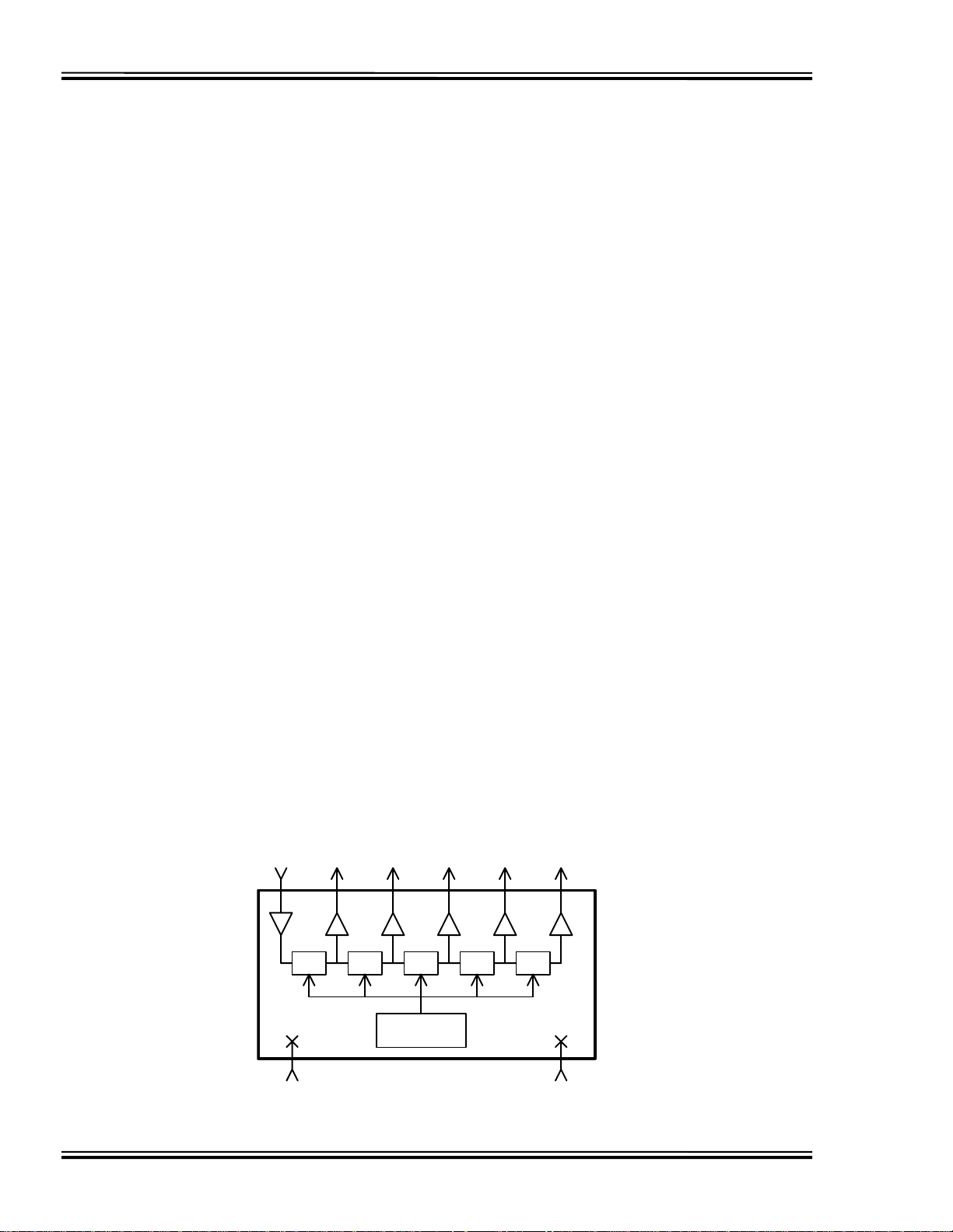
The 3D7205 five-tap delay line architecture is
shown in Figure 1. The delay line is composed
of a number of delay cells connected in series.
Each delay cell produces at its output a replica of
the signal present at its input, shifted in time.
The delay cells are matched and share the same
compensation signals, which minimizes tap-totap delay deviations over temperature and supply
voltage variations.
INPUT SIGNAL CHARACTERISTICS
The Frequency and/or Pulse Width (high or low)
of operation may adversely impact the specified
delay accuracy of the particular device. The
reasons for the dependency of the output delay
accuracy on the input signal characteristics are
varied and complex. Therefore a Maximum and
an Absolute Maximum operating input
frequency and a Minimum and an Absolute
Minimum operating pulse width have been
specified.
OPERATING FREQUENCY
The Absolute Maximum Operating Frequency
specification, tabulated in Table 1, determines
the highest frequency of the delay line input
signal that can be reproduced, shifted in time at
the device output, with acceptable duty cycle
distortion.
The Maximum Operating Frequency
specification determines the highest frequency of
the delay line input signal for which the output
delay accuracy is guaranteed.
To guarantee the Table 1 delay accuracy for
input frequencies higher than the Maximum
Operating Frequency, the 3D7205 must be
tested at the user operating frequency.
Therefore, to facilitate production and device
identification, the part number will include a
custom reference designator identifying the
intended frequency of operation. The
programmed delay accuracy of the device is
guaranteed, therefore, only at the user specified
input frequency. Small input frequency variation
about the selected frequency will only marginally
impact the programmed delay accuracy, if at all.
Nevertheless, it is strongly recommended that
the engineering staff at DATA DELAY
DEVICES be consulted.
OPERATING PULSE WIDTH
The Absolute Minimum Operating Pulse
Width (high or low) specification, tabulated in
Table 1, determines the smallest Pulse Width of
the delay line input signal that can be
reproduced, shifted in time at the device output,
with acceptable pulse width distortion.
The Minimum Operating Pulse Width (high or
low) specification determines the smallest Pulse
Width of the delay line input signal for which the
output delay accuracy tabulated in Table 1 is
guaranteed.
To guarantee the Table 1 delay accuracy for
input pulse width smaller than the Minimum
Operating Pulse Width, the 3D7205 must be
tested at the user operating pulse width.
Therefore, to facilitate production and device
identification, the part number will include a
O1IN O2 O3 O4
20% 20% 20% 20% 20%
Temp & VDD
Compensation
VDD
Figure 1: 3D7205 Functional Diagram
Doc #96007 DATA DELAY DEVICES, INC. 2
12/2/96 Tel: 973-773-2299 Fax: 973-773-9672 http://www.datadelay.com
O5
GND
 Loading...