

data delay devices 3D3701 Service Manual
3D3701
MONOLITHIC GATED
DELAY LINE OSCILLATOR
(SERIES 3D3701)
FEATURES
• All-silicon, low-power CMOS technology
• Vapor phase, IR and wave solderable
• Auto-insertable (DIP pkg.)
• Frequency range: 0.3MHz through 100MHz
• Frequency tolerance: 0.5% typical
• Temperature stability: ±1.5% typical (-40C to 85C)
• Vdd stability: ±0.5% typical (3.0V to 3.6V)
• 14-pin DIP available as drop-in replacements for
hybrid delay line oscillators
O1
NC
NC
GND
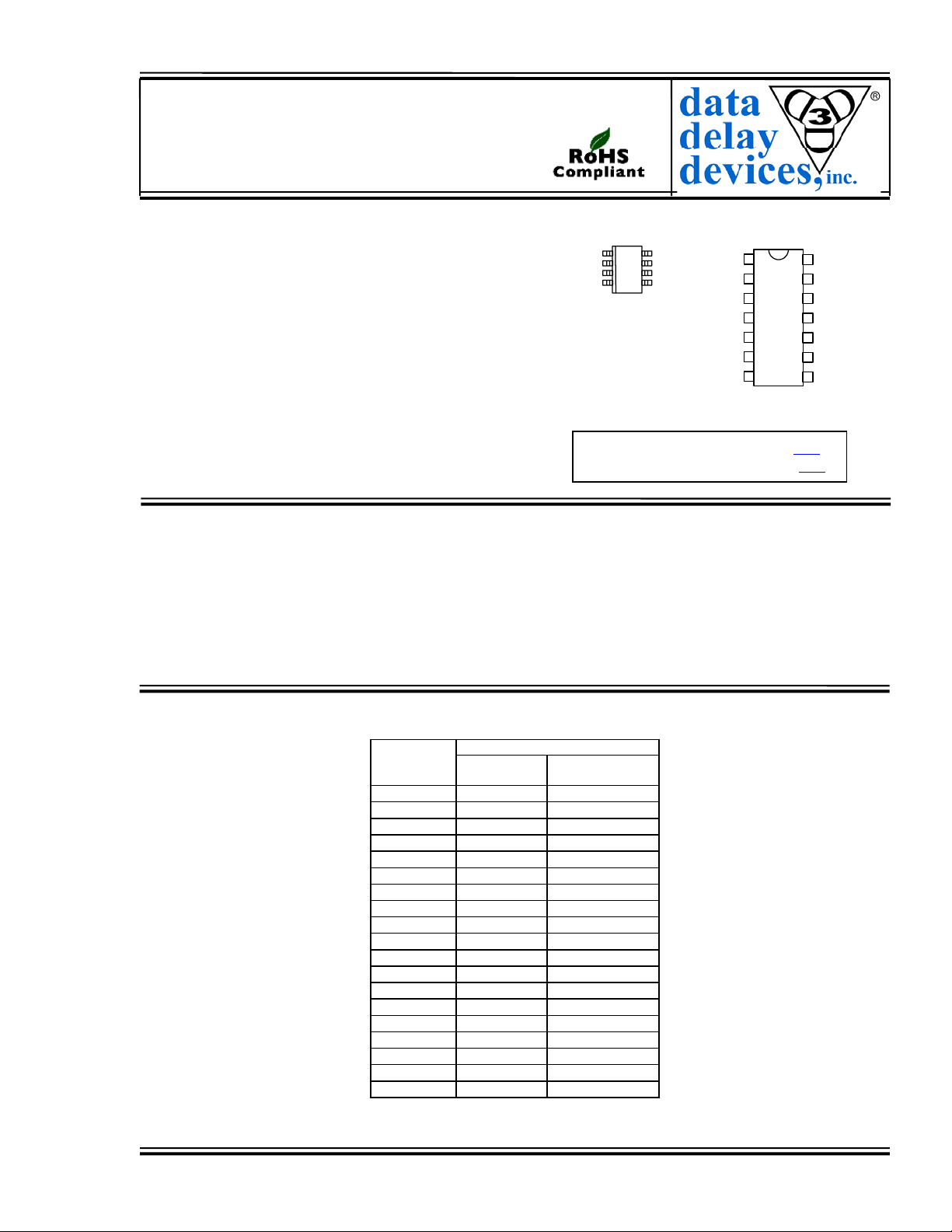
3D3701Z-xx SOIC-8
For mechanical dimensions, click here.
For package marking details, click here.
1
2
3
4
FUNCTIONAL DESCRIPTION
The 3D3701 Delay Line Oscillator product family consists of fixedfrequency CMOS integrated circuit oscillators. Each package contains a
single oscillator, which is gated and can therefore be synchronized to an
external signal. The device frequency can range from 0.3MHz through
100MHz. The 3D3701 has two outputs that are in phase when the
oscillator is running. The 3D3701 is offered in a standard 14-pin autoinsertable DIP and a space saving surface mount 8-pin SOIC package.
PACKAGES
VDD
8
NC
7
O2
6
EN
5
O1
1
NC
2
NC
3
NC
4
NC
5
NC
6
GND
3D3701-xx DIP-14
3D3701K-xx NC pins removed
7
PIN DESCRIPTIONS
EN Oscillator Enable
O1 Oscillator Output 1
O2 Oscillator Output 2
VDD +3.3 Volts
GND Ground
14
13
12
11
10
VDD
NC
NC
NC
O2
NC
9
EN
8
TABLE 1: PART NUMBER SPECIFICATIONS
NUMBER
-0.3
-0.4
-0.5
-0.75
-1
-2
-2.5
-3
-4
-5
-7.5
-10
-20
-25
-30
-40
-50
-75
NOTE: Any dash number between 0.3 and 100 not shown is also available as standard. 2006 Data Delay Devices
Doc #06026 DATA DELAY DEVICES, INC. 1
-100
OUTPUT FREQUENCY (MHz) DASH
25C
Vdd=3.3V
0.3 ± 0.002 0.3 ± 0.008
0.4 ± 0.002 0.4 ± 0.010
0.5 ± 0.003 0.5 ± 0.013
0.75 ± 0.004 0.75 ± 0.019
1.0 ± 0.005 1.0 ± 0.025
2.0 ± 0.010 2.0 ± 0.050
2.5 ± 0.013 2.5 ± 0.063
3.0 ± 0.015 3.0 ± 0.075
4.0 ± 0.020 4.0 ± 0.100
5.0 ± 0.025 5.0 ± 0.125
7.5 ± 0.038 7.5 ± 0.188
10.0 ± 0.05 10.0 ± 0.25
20.0 ± 0.10 20.0 ± 0.50
25.0 ± 0.13 25.0 ± 0.63
30.0 ± 0.15 30.0 ± 0.75
40.0 ± 0.20 40.0 ± 1.00
50.0 ± 0.25 50.0 ± 1.50
75.0 ± 0.38 75.0 ± 5.25
100.0 ± 0.50 100.0 ± 12.0
-40C to 85C
3.0V<Vdd<3.6V
12/5/2006 3 Mt. Prospect Ave. Clifton, NJ 07013
3D3701
APPLICATION NOTES
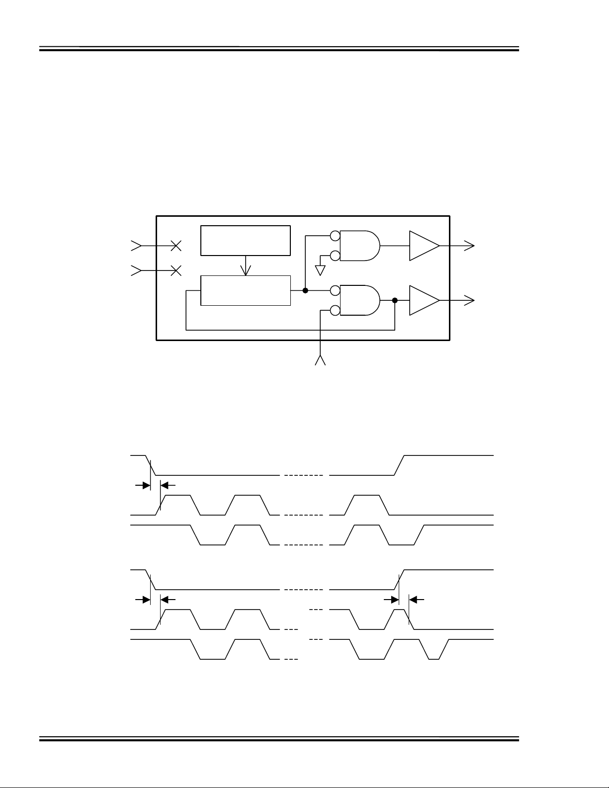
OPERATIONAL DESCRIPTION
The 3D3701 delay line oscillator architecture is
shown in Figure 1. The internal delay line is
composed of a number of delay cells connected
in series and is compensated for thermal and
supply voltage variations. A low-going edge on
the EN input starts the oscillator, with the O2
output responding immediately. The O1 output is
VDD
GND
Temp & Vdd
Compensation
Delay Line
delayed by ½ cycle. The response of the output
when the oscillator is disabled depends on the
status of O2 when the EN signal goes high, as
shown in Figure 2. If O2 is low, it will remain low,
and the final pulse on O1 will be ½ of the period.
If O2 is high, it will go low as soon as EN goes
high, and the final pulse on both outputs will have
a width smaller than ½ the period.
O1
O2
EN
Figure 1: 3D3701 Functional Diagram
EN
6ns typ
O2
O1
EN
6ns typ 6ns typ
O2
O1
Figure 2: 3D3701 Timing Diagrams
Doc #06026 DATA DELAY DEVICES, INC. 2
12/5/2006 Tel: 973-773-2299 Fax: 973-773-9672 http://www.datadelay.com
 Loading...