


PPG312F
Doc #97008 DATA DELAY DEVICES, INC. 1
1/15/97 3 Mt. Prospect Ave. Clifton, NJ 07013
12-BIT PROGRAMMABLE
PULSE GENERATOR
(SERIES PPG312F)
FEATURES PACKAGES
• Digitally programmable in 4096 steps
• Monotonic pulse-width-vs-address variation
• Rising edge triggered
• Two separate outputs: inverting & non-inverting
• Precise and stable pulse width
• Input & outputs fully TTL interfaced & buffered
• 10 T2L fan-out capability
• Fits standard 40-pin DIP socket
• Auto-insertable
FUNCTIONAL DESCRIPTION
The PPG312F-series device is a 12-bit digitally programmable pulse
generator. The width, PWA, depends on the address code (A11-A0)
according to the following formula:
PWA = PW0 + T
INC
* A
where A is the address code, T
INC
is the incremental pulse width of the
device, and PW0 is the inherent pulse width of the device. The
incremental width is specified by the dash number of the device and can range from 0.5ns through 400ns,
inclusively. RESET is held LOW during normal operation. When it is brought HIGH, OUT and OUT/ are
forced into LOW and HIGH states, respectively, and the unit is ready for the next trigger input. The
address is not latched and must remain asserted while the output pulse is active.
SERIES SPECIFICATIONS
• Programmed pulse width tolerance: 5% or 2ns,
whichever is greater
• Inherent width (PW0):20ns typical
• Inherent delay (TTO): 10ns ± 2ns
• Operating temperature: 0° to 70° C
• Supply voltage VCC: 5VDC ± 5%
• Supply current: ICC = 200ma typical
1997 Data Delay Devices
data
delay
devices, inc.
3
40
39
38
37
36
35
34
33
32
31
30
29
28
27
26
25
24
23
22
21
1
2
3
4
5
6
7
8
9
10
11
12
13
14
15
16
17
18
19
20
TRIG
N/C
N/C
N/C
N/C
N/C
N/C
GND
N/C
N/C
GND
A3
A5
A6
A7
GND
A8
A9
A10
A11
VCC
N/C
OUT
OUT/
N/C
RES
N/C
N/C
VCC
A0
A1
A2
N/C
N/C
N/C
N/C
N/C
A4
N/C
VCC
PPG312F-xx
DIP
PPG312F-xxC5
Gull-Wing
PPG312F-xxM
Military DIP
PPG312F-xxMC5
Military Gull-Wing
PIN DESCRIPTIONS
TRIG Trigger Input
OUT Non-inverted Output
OUT/ Inverted Output
A0-A11 Address Bits
RES Reset
VCC +5 Volts
GND Ground
DASH NUMBER SPECIFICATIONS
Part
Number
Incremental Width
Per Step (ns)
Total Width
Change (us)
PPG312F-.5
.5 ± .3 2.048 ± 0.10
PPG312F-1
1 ± .5 4.096 ± 0.20
PPG312F-2
2 ± .5 8.192 ± 0.41
PPG312F-5
5 ± 1.5 20.48 ± 1.02
PPG312F-10
10 ± 2.0 40.96 ± 2.05
PPG312F-20
20 ± 2.0 81.92 ± 4.10
PPG312F-50
50 ± 2.5 204.8 ± 10.2
PPG312F-100
100 ± 5.0 409.6 ± 20.5
PPG312F-200
200 ± 10.0 819.2 ± 41.0
PPG312F-400
400 ± 20.0 1,638.4 ± 81.9
NOTE: Any dash number between .5 and 400 not
shown is also available.
PPG312F
Doc #97008 DATA DELAY DEVICES, INC. 2
1/15/97 Tel: 973-773-2299 Fax: 973-773-9672 http://www.datadelay.com
APPLICATION NOTES
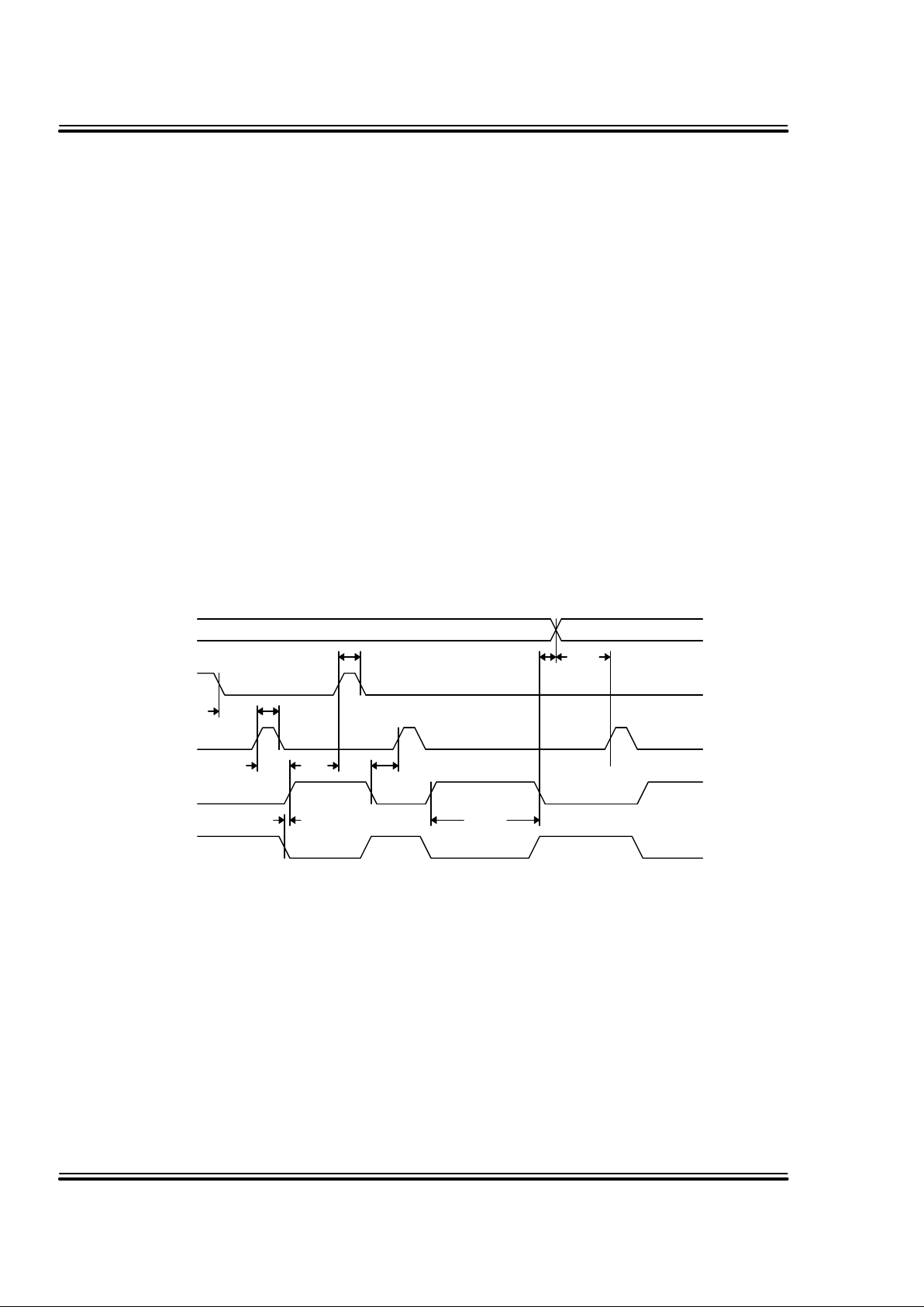
DEVICE TIMING
The timing definitions and restrictions for the
PPG312F are shown in Figure 1. The unit is
activated by a rising edge on the TRIG input.
After a time, TTO (called the inherent delay), the
rising edge of the pulse appears at OUT. The
duration of the pulse is given by the above
equation. For the duration of the pulse, the
device ignores subsequent triggers. Once the
falling edge of the pulse has appeared at OUT,
an additional time, T
OTR
, is required before the
device can respond to the next trigger.
At power-up, the state of the PPG312F is
unknown. Consequently, after power is applied,
the unit may not respond to input triggers for a
time equal to the maximum pulse width, PWT.
After this time, the unit will function properly. If
your application requires that the device function
immediately, issue a quick reset at power-up.
POWER SUPPLY BYPASSING
The PPG312F relies on a stable power supply to
produce repeatable pulses within the stated
tolerances. A 0.1uf capacitor from VCC to GND,
located as close as possible to each VCC pin, is
recommended. A wide VCC trace should
connect all VCC pins externally, and a clean
ground plane should be used.
INCREMENT TOLERANCES
Please note that the increment tolerances listed
represent a design goal. Although most
increments will fall within tolerance, they are not
guaranteed throughout the address range of the
unit. Monotonicity is, however, guaranteed over
all addresses.
`
T
OAX
T
RTS
T
TW
T
TO
PW
A
A11-A0
RES
TRIG
OUT
OUT/
Figure 1: Timing Diagram
A
i
A
i+1
T
SKEW
T
ATS
T
RO
T
OTR
T
TW
T
RW

PPG312F
Doc #97008 DATA DELAY DEVICES, INC. 3
1/15/97 3 Mt. Prospect Ave. Clifton, NJ 07013
DEVICE SPECIFICATIONS
TABLE 1: AC CHARACTERISTICS
PARAMETER SYMBOL MIN TYP MAX UNITS
Total Programmable Pulse Width PW
T
4095 T
INC
Inherent Pulse Width PW
0
15.0 20.0 27.0 ns
Trigger to Output Delay T
TO
8.0 10.0 12.0 ns
Reset to Output Delay T
RO
17.0 ns
Output Skew T
SKEW
1.5 ns
Trigger Pulse Width T
TW
5.0 ns
Reset Pulse Width T
RW
10.0 ns
Reset to Trigger Setup Time T
RTS
9.0 ns
Address to Trigger Setup Time T
ATS
6.0 ns
Output Low to Address Change T
OAX
0.0 ns
Output to Trigger Recovery Time T
OTR
10.0 ns
TABLE 2: ABSOLUTE MAXIMUM RATINGS
PARAMETER SYMBOL MIN MAX UNITS NOTES
DC Supply Voltage V
CC
-0.3 7.0 V
Input Pin Voltage V
IN
-0.3 VDD+0.3 V
Storage Temperature T
STRG
-55 150 C
Lead Temperature T
LEAD
300 C 10 sec
TABLE 3: DC ELECTRICAL CHARACTERISTICS
(0C to 70C, 4.75V to 5.25V)
PARAMETER SYMBOL MIN TYP MAX UNITS NOTES
High Level Output Voltage V
OH
2.5 3.4 V VCC = MIN, IOH = MAX
VIH = MIN, VIL = MAX
Low Level Output Voltage V
OL
0.35 0.5 V VCC = MIN, IOL = MAX
VIH = MIN, VIL = MAX
High Level Output Current I
OH
-1.0 mA
Low Level Output Current I
OL
20.0 mA
High Level Input Voltage V
IH
2.0 V
Low Level Input Voltage V
IL
0.8 V
Input Clamp Voltage V
IK
-1.2 V VCC = MIN, II = I
IK
Input Current at Maximum
Input Voltage
I
IHH
0.1 mA VCC = MAX, VI = 7.0V
High Level Input Current I
IH
20
µA
VCC = MAX, VI = 2.7V
Low Level Input Current I
IL
-0.6 mA VCC = MAX, VI = 0.5V
Short-circuit Output Current I
OS
-60 -150 mA VCC = MAX
Output High Fan-out 25 Unit
Output Low Fan-out 12.5 Load

PPG312F
Doc #97008 DATA DELAY DEVICES, INC. 4
1/15/97 Tel: 973-773-2299 Fax: 973-773-9672 http://www.datadelay.com
PACKAGE DIMENSIONS
2.100 MAX.
1 2 3 4 5 6 7 8 161514131211109
.320
MAX.
.015 TYP.
.070 MAX.
.018 TYP.
.580
MAX.
.650
MAX.
.010
±.002
Lead Material:
Nickel-Iron alloy 42
TIN PLATE
20191817
24 23 22 2129303132333435 252627283637383940
.100 TYP.
DIP (PPG312F-xx, PPG312F-xxM)
2.080±.020
.882
±.005
.020 TYP.
.040 TYP.
.100
.090
1.100
.320
MAX.
.590
MAX.
.010±.002
.050
±.010
.710
±.005
.007
±.005
1 2 3 4 5 6 7 8 9 10 11 12 13 14 15 16 17 18 19 20
2122232425262728293031323334353637383940
Gull-Wing (PPG312F-xxC5, PPG312F-xxMC5)

PPG312F
Doc #97008 DATA DELAY DEVICES, INC. 5
1/15/97 3 Mt. Prospect Ave. Clifton, NJ 07013
DELAY LINE AUTOMATED TESTING
TEST CONDITIONS
INPUT: OUTPUT:
Ambient Temperature: 25oC ± 3oC Load: 1 FAST-TTL Gate
Supply Voltage (Vcc): 5.0V ± 0.1V C
load
: 5pf ± 10%
Input Pulse: High = 3.0V ± 0.1V Threshold: 1.5V (Rising & Falling)
Low = 0.0V ± 0.1V
Source Impedance: 50Ω Max.
Rise/Fall Time: 3.0 ns Max. (measured
between 0.6V and 2.4V )
Pulse Width: PWIN = 10ns
Period: PERIN = 2 x Max. Pulse Width
NOTE: The above conditions are for test only and do not in any way restrict the operation of the device.
OUT
OUT
TRIGINREF
TRIG
Test Setup
DEVICE UNDER
TEST (DUT)
TIME INTERVAL
COUNTER
PULSE
GENERATOR
COMPUTER
SYSTEM
PRINTER
IN
Timing Diagram For Testing
T
TO
PW
A
PER
IN
PW
IN
T
RISE
T
FALL
0.6V
0.6V
1.5V
1.5V
2.4V
2.4V
1.5V
1.5V
V
IH
V
IL
V
OH
V
OL
INPUT
SIGNAL
OUTPUT
SIGNAL
 Loading...