

Datacom DM991C, DM991S, DM991SE, DM991CE Product Manual

DM991 SERIES V
DM991C
DM991CE
DM991S
DM991SE
PRODUCT MANUAL
204.4092.08 rev. 08 Date: 8/12/2008

WARRANTY
This product is guaranteed to be free against manufacturing and raw material defects, during the period
specified in the sales receipt.
The warranty includes only the repair and replacement of components or defective parts, free of charge.
The warranty does not cover damages caused by any one of the following conditions: improper use,
energy failures, natural phenomena (lightning, for example), failure in equipments connected to this
product, improper grounding or repairs done by DATACOM unauthorized personnel.
This warranty does not cover repairs done at the customer’s site. All equipments must be sent to
DATACOM to be repaired.
Quality Management System
certified by DQS according to ISO9001
Register number (287097 QM)
Although this document has been written with care, the company does not assume responsibility for
occasional mistakes and omissions in its content. Likewise, DATACOM is not liable for any damages that
may result from the use of the information contained in this manual. Specifications provided in this manual
are subject to changes without any previous notice and should not be construed as a commitment of any
kind by DATACOM.

CONTACTS
In order to contact the DATACOM technical support, or sales department:
Support
o E-mail: suporte@datacom.ind.br
o Phone: +55 51 3358-0122
o Fax: +55 51 3358-0101
• Sales
o E-mail: comercial@datacom.ind.br
o Phone: +55 51 3358-0100
o Fax: +55 51 3358-0101
• Internet
o www.datacom.ind.br
• Address
o DATACOM
o Av. França, 735 - Porto Alegre, RS - Brasil
o CEP: 90230-220
CONVENTIONS
In order to improve the agreement, the following conventions are made throughout this manual:
hyperlink - Indicates an internet site or an e-mail address.
Command or Button - Always that some reference to a command, a button or a software menu is
made, this indication will be in italic.
# Commands and messages from terminal screens are presented in not-
formatted text, preceded from #.
Notes give an explanation about some topic in the foregoing paragraph.
This symbol means that this text is very important and, if the orientations were not correct follo
wed, it may
cause damage or hazard.
This symbols means that, case the procedure was not correctly followed, may exist electrical shock risk.
Represents laser radiation. It is necessary to avoid eye and skin exposure.
In
dicates that an equipment or a part is ESDS (Electrostatic Discharge Sensitive). It should not be
handled without grounding wrist strap or equivalent.
Non-ionizing radiation emission.
IWEEE Directive Symbol (Applicable in the European Un
ion and other European countries with separate
collection systems).This symbol on the product or its packaging indicates that this product must not be
disposed of with other waste. Instead, it is your responsibility to dispose of your waste equipment by
ha
nding it over to a designated collection point for the recycling of waste electrical and electronic
equipment. The separate collection and recycling of your waste equipment at the time of disposal will help
conserve natural resources and ensure that it is
recycled in a manner that protects human health and the
environment. For more information about where you can drop off your consumer waste equipment for
recycling, please contact your local city recycling office or the dealer from whom you originally purch
ased
the product

INDEX
1. GENERAL RECOMMENDATION.................................................10
2. INTRODUCTION..........................................................................11
2.1. DM991S/SE 2W/4W............................................................................................. 11
2.1.1. Front Panel.................................................................................................................................. 11
2.1.2. Back Panel .................................................................................................................................. 12
2.2. DM991C/CE 2W/4W ............................................................................................ 13
2.2.1. Front Panel.................................................................................................................................. 13
2.2.2. Back Panel .................................................................................................................................. 14
3. G.SHDSL INTERFACE ................................................................15
3.1. Interface Characteristics....................................................................................... 16
3.2. Handshake (Pre-activation).................................................................................. 16
3.3. Training (Activation) ............................................................................................. 16
3.4. Data Mode............................................................................................................ 17
3.4.1. G.shdsl Frame Structure ............................................................................................................. 17
3.4.2. CRC Anomaly.............................................................................................................................. 18
3.4.3. Loop Attenuation Defect.............................................................................................................. 18
3.4.4. SNR Margin Defect...................................................................................................................... 19
3.4.5. LOSW Defect .............................................................................................................................. 19
3.4.6. LOSW Failure.............................................................................................................................. 19
3.5. G.shdsl Interface Configurations.......................................................................... 19
3.5.1. Terminal Type.............................................................................................................................. 19
3.5.2. Frame Mode ................................................................................................................................ 19
3.5.3. Annex .......................................................................................................................................... 20
3.6. Performance ........................................................................................................ 20
3.7. Four wire operation (4W)...................................................................................... 21
3.7.1. Operating on two wires................................................................................................................ 21
3.7.2. Operating on four wires: .............................................................................................................. 21
3.8. Electrical Protection.............................................................................................. 21
4. V.35-V36/V.11 DIGITAL INTERFACE..........................................22
5. G.703 - G.704 INTERFACE .........................................................25
5.1. DM991S/SE ......................................................................................................... 25
5.2. DM991C/CE......................................................................................................... 26
6. ETHERNET INTERFACE.............................................................27
6.1. Ethernet physical level.......................................................................................... 27
6.2. Remote Bridge..................................................................................................... 27
6.3. Ethernet Interface Configurations......................................................................... 27
7. STRAPS.......................................................................................29
7.1. DM991S/SE ......................................................................................................... 29
7.1.1. G.703 Interface Cable Selection (E4).......................................................................................... 29
7.1.2. Output Coaxial Cable Grounding (E10)....................................................................................... 29
7.1.3. Input Coaxial Cable Grounding (E11).......................................................................................... 29
7.1.4. G.703 Interface Pinout (E12 to E15, E27 to E30 and E44 to E47).............................................. 29
7.1.5. Digital Interface Selection (E16, E18 and E20) ........................................................................... 30
7.1.6. DB25 Connector Pinout (E31 to E41 and E48 to E59)................................................................ 30
7.2. DM991C/CE......................................................................................................... 30
7.2.1. G.703 Interface Cable Selection (E2, E3 and E25)..................................................................... 30
7.2.2. Input Coaxial Cable Grounding (E4)............................................................................................ 30
7.2.3. Output Coaxial Cable Grounding (E5)......................................................................................... 30
7.2.4. Digital Interface Selection (E10, E12 and E13) ........................................................................... 31
7.2.5. Pinning on connector DB25 (E500 to E522) – Optional .............................................................. 31
8. DIP-SWITCHES...........................................................................32
8.1. Speed Selection (DIPs A1 to A5) ......................................................................... 32
8.2. Clock Selection (DIPs A6 and A7)........................................................................ 33
8.3. LDR Enabling (DIP A8) ........................................................................................ 34
8.4. Cross-Connect CAS (DIP B1) .............................................................................. 34

8.5. Timeslot 16 Enabling (DIP B2) ............................................................................. 34
8.6. CRC4 Enabling (DIP B3)...................................................................................... 34
8.7. E1/Digital interface selection (DIP B4).................................................................. 34
8.8. Terminal type (DIP B5)......................................................................................... 35
8.9. Configuration (DIP B6)......................................................................................... 35
8.10. Converter Mode / Ethernet interface enabling (DIP B7)...................................... 35
8.10.1. DM991S..................................................................................................................................... 35
8.10.2. DM991SE .................................................................................................................................. 35
8.11. Four wire operation ............................................................................................ 35
8.12. DIPs Summary................................................................................................... 36
9. OPERATION DESCRIPTION.......................................................37
9.1. Equipment Management ...................................................................................... 37
9.2. Equipment Clocks ................................................................................................ 37
9.2.1. Transmission Clock..................................................................................................................... 37
9.2.2. Plesiochronous Mode.................................................................................................................. 38
9.2.3. Synchronous Mode...................................................................................................................... 39
9.3. Digital Interface Clocks......................................................................................... 39
9.3.1. Clock Source ............................................................................................................................... 39
9.3.2. External (CT113) ......................................................................................................................... 39
9.3.3. CT104 sinc. CT113...................................................................................................................... 40
9.3.4. CT113 Unlooped to CT114.......................................................................................................... 40
9.3.5. CT128 Enabled............................................................................................................................ 41
9.3.6. Invert Tx Clock............................................................................................................................. 41
9.4. Converter Mode.................................................................................................... 41
10. TERMINAL MANAGEMENT.........................................................42
10.1. Equipment Information ....................................................................................... 43
10.2. Password Configuration ..................................................................................... 44
10.3. Language Configuration..................................................................................... 44
10.4. Choosing Equipment to be Configured............................................................... 45
10.5. Configuration Menu............................................................................................ 46
10.5.1. Equipment General Configurations Menu ................................................................................. 48
10.5.2. G.shdsl Interface Configuration Menu....................................................................................... 49
10.5.3. Digital Interface Configuration Menu ......................................................................................... 50
10.5.4. E1 Interface Configuration Menu............................................................................................... 51
10.5.5. Bridge Interface Configuration Menu (only for DM991CE and DM991SE)................................ 52
10.6. Test Menu.......................................................................................................... 52
10.6.1. G.shdsl Interface Test Menu ..................................................................................................... 54
10.6.2. Digital Interface Test Menu........................................................................................................ 54
10.6.3. E1 Interface Test Menu ............................................................................................................. 55
10.7. Status Menu....................................................................................................... 55
10.7.1. Equipment Status Menu............................................................................................................ 56
10.7.2. G.shdsl Interface Status Menu.................................................................................................. 56
10.7.3. Digital Interface Status Menu .................................................................................................... 57
10.7.4. E1 Interface Status Menu.......................................................................................................... 58
10.7.5. Bridge Interface Status Menu.................................................................................................... 59
10.8. Performance Menu............................................................................................. 59
10.9. Terminal Firmware Download............................................................................. 60
11. REMOTE MANAGEMENT............................................................61
12. TESTS..........................................................................................62
12.1. G.shdsl Interface Tests ...................................................................................... 62
12.1.1. Local Digital Loopback Test- LDL.............................................................................................. 62
12.1.2. Local Analogue Loopback Test - LAL........................................................................................ 62
12.1.3. BERT Test................................................................................................................................. 62
12.1.4. RDL Test ................................................................................................................................... 63
12.2. E1 Interface Tests.............................................................................................. 63
12.2.1. LDL Test.................................................................................................................................... 63
12.2.2. LAL Test .................................................................................................................................... 63
12.3. Digital Interface Tests ........................................................................................ 64
12.3.1. LDL Test.................................................................................................................................... 64

13. CONVERTER MODE TESTS.......................................................65
13.1. Local Analogue Loopback - LAL........................................................................ 65
13.2. Local Digital Loopback Test - LDL...................................................................... 65
14. FIRMWARE DOWNLOAD............................................................67
15. INSTALLATION AND OPERATION .............................................68
15.1. Installation.......................................................................................................... 68
15.1.1. DM991S/SE............................................................................................................................... 68
15.1.2. DM991C/CE............................................................................................................................... 68
15.2. Operation ........................................................................................................... 68
15.3. Accessory........................................................................................................... 69
15.3.1. Adapter Cable DB25 X DB25 2BNC.......................................................................................... 69
16. G.703 - G.704 ..............................................................................70
16.1. G.704 Frame structure ....................................................................................... 70
16.1.1. CRC4 Multiframe....................................................................................................................... 71
16.1.2. CAS Multiframe (Channel Associated Signaling) ...................................................................... 72
16.2. Electrical Characteristics.................................................................................... 73
16.2.1. G.703 Interface Electrical Characteristics for Coaxial Cable..................................................... 74
16.2.2. G.703 Interface Electricial Characteristics for Twisted Pair....................................................... 74
17. PANEL LEDS...............................................................................75
17.1. DM991S/SE Modems Front Panel LEDs............................................................ 75
17.2. DM991C/CE Modems Front Panel LEDs............................................................ 76
18. STRAPS AND DIP SWITCHES MAP...........................................78
18.1. DM991S/SE ....................................................................................................... 78
18.2. DM991C/CE....................................................................................................... 78
18.2.1. PCI rev. 03 or lesser.................................................................................................................. 79
18.2.2. PCI rev. 04 or higher ................................................................................................................. 80
19. TECHNICAL SPECIFICATIONS ..................................................81
19.1. Environmental Conditions................................................................................... 81
19.2. Power................................................................................................................. 81
19.2.1. DM991S/SE............................................................................................................................... 81
19.2.2. DM991C/CE............................................................................................................................... 81
19.3. Power Input........................................................................................................ 81
19.3.1. DM991S/SE............................................................................................................................... 81
19.3.2. DM991C/CE............................................................................................................................... 82
19.4. Dimensions ........................................................................................................ 83
19.4.1. DM991S/SE............................................................................................................................... 83
19.4.2. DM991C/CE............................................................................................................................... 83
19.5. Weight................................................................................................................ 83
19.5.1. DM991S/SE............................................................................................................................... 83
19.5.2. DM991C/CE............................................................................................................................... 83
20. APPLICABLE STANDARDS.........................................................84
21. ANNEX I – SAFETY WARNINGS.................................................85
22. ANLAGE 2 - SICHERHEITSHINWEISE......................................87

FIGURE INDEX
Figure 1. Front Panel - DM991S 2W ......................................................................11
Figure 2. Front Panel - DM991SE 2W....................................................................12
Figure 3. Front Panel - DM991S 4W ......................................................................12
Figure 4. Front Panel - DM991SE 4W....................................................................12
Figure 5. DM991S/SE Back Panel..........................................................................12
Figure 6. DM991C 2W Front Panel ........................................................................13
Figure 7. DM991CE 2W Front Panel......................................................................13
Figure 8. DM991C 4W Front Panel ........................................................................13
Figure 9. DM991CE 4W Front Panel......................................................................13
Figure 10. DM991C/CE Back Panel......................................................................14
Figure 11. G.shdsl frame order diagram with CAS signaling .................................17
Figure 12. G.shdsl frame order diagram with CAS signaling .................................17
Figure 13. G.shdsl Interface Reach (m X kbit/s)....................................................21
Figure 14. DM991 Managed as DM705 remote.....................................................37
Figure 15. Internal and Regenerated Clocks in Plesiochronous Mode ..................38
Figure 16. E1 External Clock and Regenerated in Plesiochronous Mode..............38
Figure 17. Digital interface External Clocks in Plesiochronous Mode....................39
Figure 18. Digital Interface Operation with Clock Source ......................................39
Figure 19. Digital Interface Operating with External ..............................................40
Figure 20. Digital Interface Operation with CT104 sinc. CT113.............................40
Figure 21. Digital Interface with CT113 Unlooped to CT114..................................41
Figure 22. Configuration memories diagram .........................................................46
Figure 23. DM991 - Local Digital Loopback on G.shdsl Interface..........................62
Figure 24. DM991 - Local Analogue Loopback Test on G.shdsl Interface.............62
Figure 25. DM991 - BERT Test on G.shdsl Interface ............................................63
Figure 26. DM991 - RDL Test on G.shdsl interface...............................................63
Figure 27. DM991 - LDL Test on E1 Interface.......................................................63
Figure 28. DM991 - LAL Test on E1 Interface.......................................................64
Figure 29. DM991 – LDL on Digital interface.........................................................64
Figure 30. LAL test Converter Mode......................................................................65
Figure 31. LDL Test Converter Mode....................................................................66
Figure 32. Adapter Cable DB25 x DB25 2BNC......................................................69
Figure 33. ITU-T G.707 E1 frame structure recommendation ...............................70
Figure 34. HDB3 coding in the G.703 2048kbit/s Interface....................................74
Figure 35. DM991S/SE - Straps and DIPs map.....................................................78
Figure 36. DM991C/CE – Map of Straps (PCI rev. 03 ou inferior) .........................79
Figure 37. DM991C/CE – Map of Straps (PCI rev. 03 ou superior) .......................80
Figure 38. Power Cable Pinout - DM991C/CE.......................................................82

TABLE INDEX
Table 1. DM991S/SE - DB9 Connector Pinout......................................................12
Table 2. DM991SE - RJ45 Connector Pinout........................................................12
Table 3. DM991C/CE - DB9 Connector Pinout......................................................14
Table 4. DM991CE - RJ45 Connector Pinout........................................................14
Table 5. DM991S/SE - G.shdsl Interface Pinout....................................................15
Table 6. DM991C/CE - G.shdsl Interface Pinout ...................................................15
Table 7. Modulation and power on the line............................................................16
Table 8. G.shdsl Frame Structure .........................................................................18
Table 9. G.shdsl Interface Reach..........................................................................20
Table 10. V.35 Interface Pinout...............................................................................23
Table 11. V.35 Interface Pinout...............................................................................24
Table 12. DM991S/SE - Pinout in the G.703 Screw connector block.......................25
Table 13. DM991S/SE - G.703 Telebrás (DB25) Standard Pinout...........................25
Table 14. DM991S/SE - G.703 Proprietary Pinout (DB25) ......................................26
Table 15. DM991C/CE - G.703 RJ48 Pinout...........................................................26
Table 16. Digital Interface Speed Configuration......................................................33
Table 17. Internal Clock Selection of Equipment.....................................................33
Table 18. DM991S/SE – DIPs Summary.................................................................36
Table 19. Multiframe structure.................................................................................71
Table 20. CRC4 multiframe structure......................................................................72
Table 21. CAS Multiframe Structure........................................................................73
Table 22. LEDs Meaning - DM991S/SE..................................................................75
Table 23. LEDs meaning - DM991C/CE..................................................................76
Table 24. Current Maximum Consumption - DM991S/SE........................................82
Table 25. Power Input Range - DM991C/CE...........................................................82
Product Manual - DM991 Series V Family - 204.4092.08 10
1. GENERAL RECOMMENDATION
Before the installation, read the entire manual attentively.
Always observe the instructions of security during the installation, operation or maintenance of this
product. Installation, adjustment or maintenance
must be carried through only by qualified, trained and
authorized people.
The installation of any electric equipment must be in accordance with the current law in the place where
this equipment will be installed. This includes adequate devices o
f protection, sizing and protection to the
capacities of the equipment.
The power supply, where the supply cable is connected, must be positioned near the equipment and be
on an easily accessible location, because the equipment is turned on and off through it
.
Before connecting any cable to the equipment, make sure that the grounding system is functional.
To prevent risks of electric shock, before opening the DM991C/CE equipments, disconnect the
power
supply.
Follow attentively every guidance included in this manual. In case of doubts, please con
tact the
authorized technical support.
The described equipment in this manual is sensible to the static electricity. Before handling any described
equi
pment in this manual, verify if using devices of protection against static electricity, and if these are
functioning correctly.
Product Manual - DM991 Series V Family - 204.4092.08 11
2. INTRODUCTION
The modem family DM991 series V has several G.SHDSL modem models, with E1 (G.703 and G.704),
Digital (V.35 and V.36/V.11) and Ethernet (10/100BaseT) interfaces.
They come in eight models:
• DM991C 2W – Desktop. Can be adapted in a sub rack, using the accessory: desktop sub-
rack adaptor. Its G.shdsl interface works on 2 wires.
• DM991C 4W – Desktop. Can be adapted in a sub rack, using the accessory: desktop sub-
rack adaptor. Its G.shdsl interface may operate with 2 or 4 wires.
• DM991CE 2W – The same as the DM991C model, however it has the option to work as
Bridge as well. Its G.shdsl interface works on 2 wires.
• DM991CE 4W – The same as the DM991C model, however it has the option to work as
Bridge as well. Its G.shdsl interface may operate with 2 or 4 wires.
• DM991S 2W – Telebrás standard card. Can be used in cabinets or sub racks standard for
20 modems. Its G.shdsl interface works on 2 wires.
• DM991S 4W – Telebrás standard card. Can be used in cabinets or sub racks standard for
20 modems. Its G.shdsl interface may operate with 2 on 4 wires.
• DM991SE 2W - The same as the DM991S model, however it has the option to work as
Bridge as well. Its G.shdsl interface works on 2 wires.
• DM991SE 4W - The same as the DM991S model, however it has the option to work as
Bridge as well. Its G.shdsl interface may operate with 2 or 4 wires.
In this manual the name DM991 will always be used to represent the entire modem family and whenever
an explanation is restricted to certain models, such model will be clearly identified.
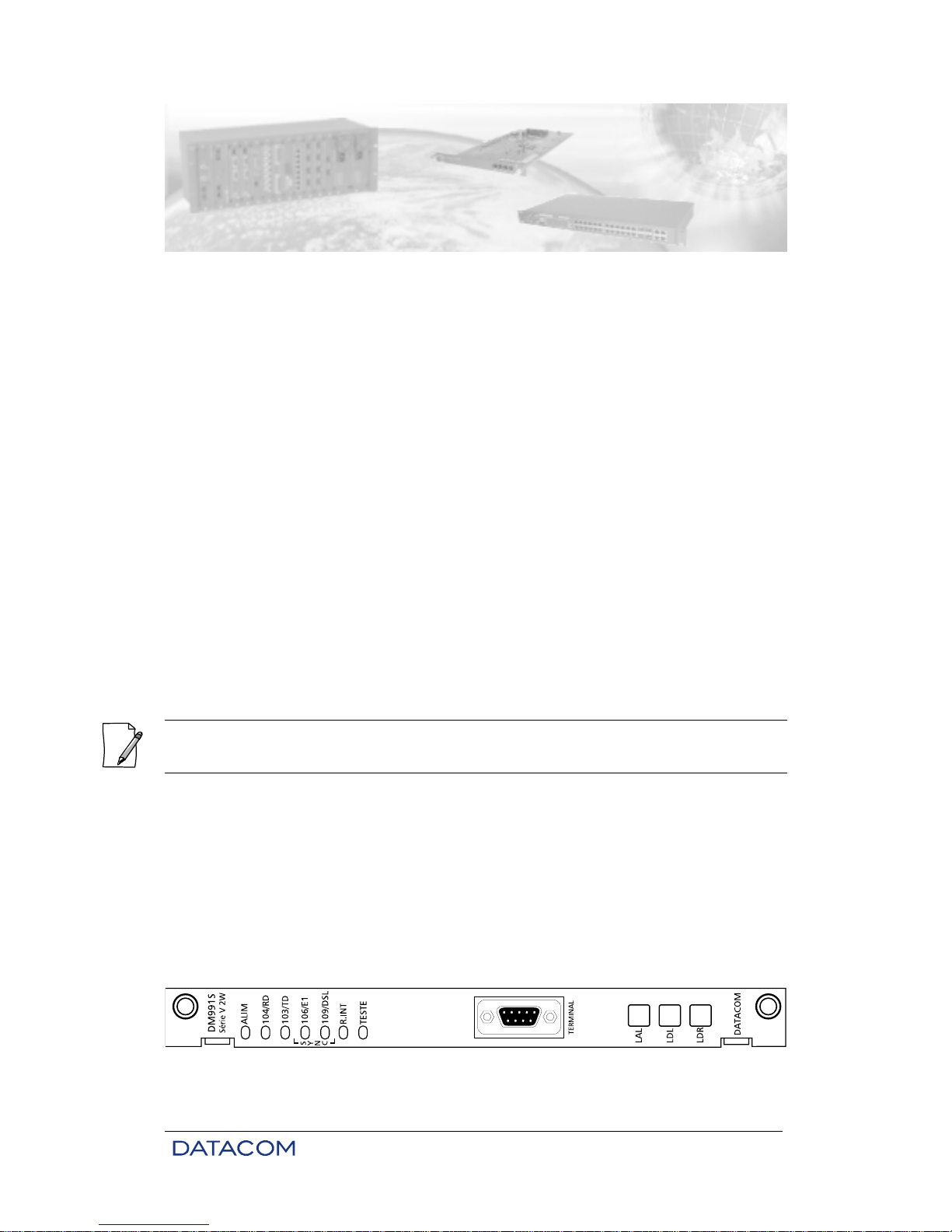
2.1. DM991S/SE 2W/4W
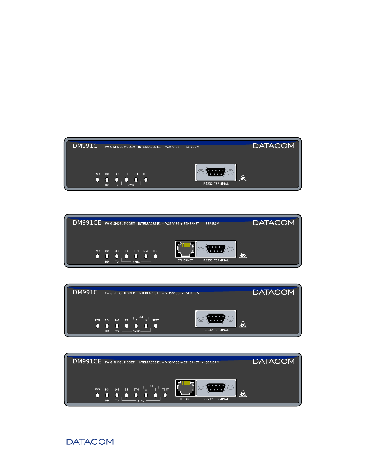
2.1.1. Front Panel
Figure 1 represents the front panel of the DM991S 2W modem, the Figure 2 presents the front panel of
the DM991SE 2W modem, Figure 3 presents the front panel of the DM991S 4W modem and the Figure 4
presents the front panel of the DM991SE 4W modem.
Figure 1. Front Panel - DM991S 2W
The letter "C", represents that the equipment is a table equipment, while the letter "S" represents that it
is
a card to be used in a Telebrás standard cabinet or shelf. The letter "E" present indicates B
ridge mode
operation.
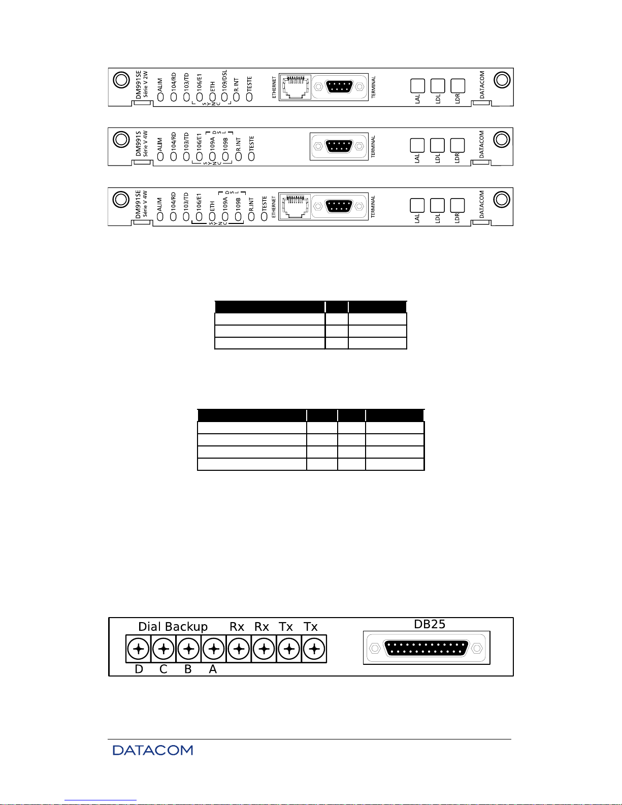
Product Manual - DM991 Series V Family - 204.4092.08 12
Figure 2. Front Panel - DM991SE 2W
Figure 3. Front Panel - DM991S 4W
Figure 4. Front Panel - DM991SE 4W
• Signaling LEDs –The meaning of each LED can be found on Table 22.
• DB9 - The DB9 connector in the front panel is used to configure the equipment via
terminal (communication serial port). The connector pinout is found on Table 1.
Signal DB9 Origin
Transmission RS-232 2 DM991S/SE
Reception RS-232 3 ETD
Ground signal 5 -
Table 1. DM991S/SE - DB9 Connector Pinout
• RJ45 - The RJ45 connector is used for the Ethernet interface. Its pinout description is
found on Table 2.
Function
Signal
RJ45 Origin
Received data: - wire OUT - 1 DM991SE
Received data: + wire OUT+ 2 DM991SE
Transmited data: + wire IN+ 3
LAN
Transmited data: - wire
IN - 6 LAN
Table 2. DM991SE - RJ45 Connector Pinout
• Keys - The keys function is the testing execution:
o LAL (Local Analogue Loopback)
o LDL (Local Digital Loopback)
o LDR (Local Digital Remote)
2.1.2. Back Panel
Figure 5 represents the back panel of the DM991S/SE modems (Telebrás standard sub-rack):
Figure 5. DM991S/SE Back Panel
• For the DB25 connector pinout, see table 11 in the chapter on the V.35 interface.
Product Manual - DM991 Series V Family - 204.4092.08 13
• Both TX pind are used for port A in the DSL interface. Both RX pins are used for port B in
the DSL interface (for model 4W only). More details are provided in the Table 5.
• Dial Backup pins are used for the E1 interface. Pins A and B are for interface input (IN)
and pins C and D are for interface output (OUT). More details are provided in the Table
12.
2.2. DM991C/CE 2W/4W
2.2.1. Front Panel
The Figure 6 represents the DM991C 2W modem panel, Figure 7 represents the DM991CE 2W modem
panel, Figure 8 presents the DM991C 4W modem and the Figure 9 presents the DM991CE 4W modem
Figure 6. DM991C 2W Front Panel
Figure 7. DM991CE 2W Front Panel
Figure 8. DM991C 4W Front Panel
Figure 9. DM991CE 4W Front Panel
Product Manual - DM991 Series V Family - 204.4092.08 14
• Signaling LEDs –The meaning of each LED can be found on Table 23.
• DB9 - The DB9 connector in the front panel is used to configure the equipment via
terminal (communication serial port). The connector pinout is found on Table 3.
Signal DB9 Orign
Transmission RS-232 2 DM991C/CE
Reception RS-232 3 ETD
Ground signal 5 -
Table 3. DM991C/CE - DB9 Connector Pinout
• RJ45 - The RJ45 connector is used as Ethernet interface. Its pinout description is found
on Table 4.
Function Signal RJ45 Origin
Received data: + wire OUT+ 1 DM991CE
Received data: - wire OUT- 2 DM991CE
Transmited data: + wire IN+ 3
LAN
Transmited data: - wire
IN- 6 LAN
Table 4. DM991CE - RJ45 Connector Pinout
2.2.2. Back Panel
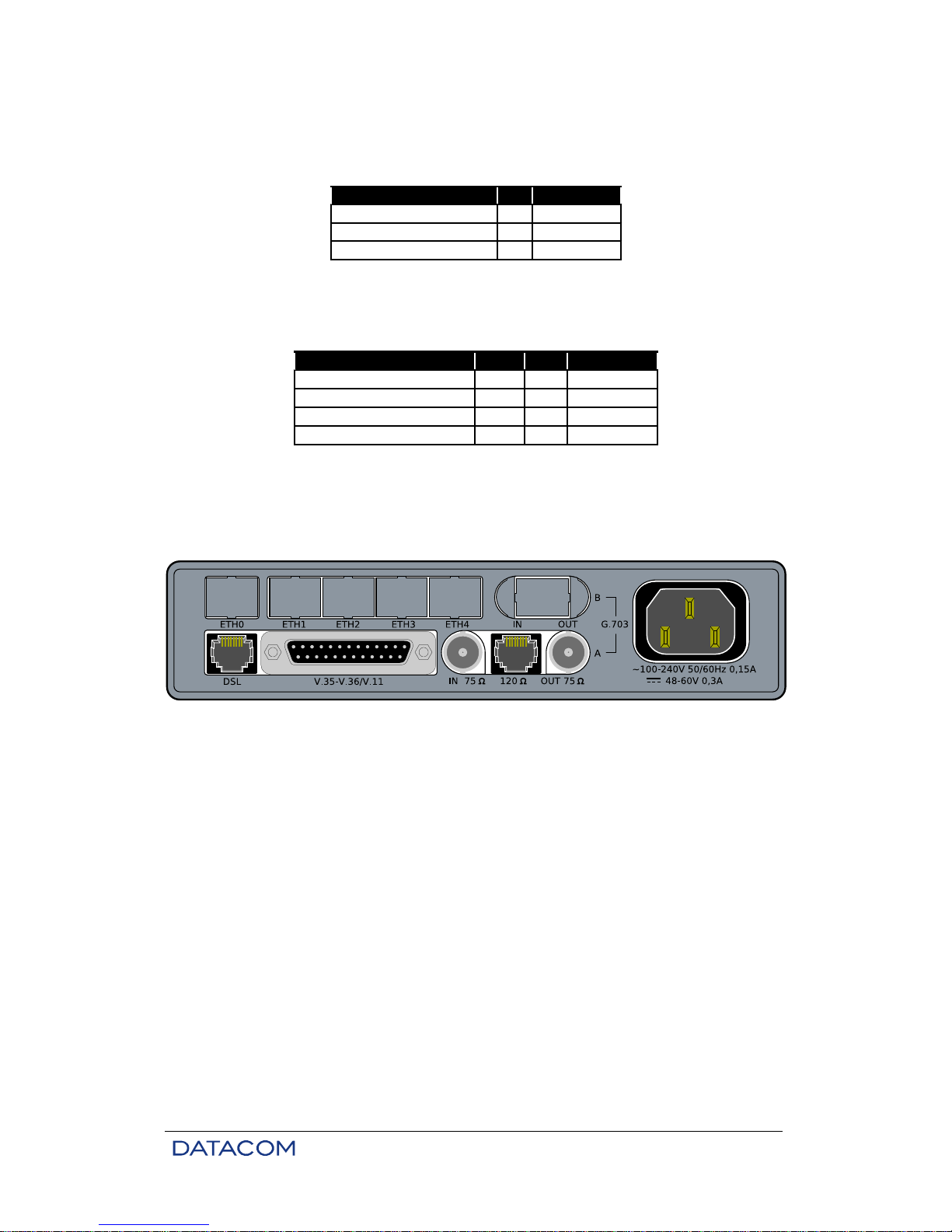
Figure 10 represents the back panel of the DM991C/CE modens:
Figure 10. DM991C/CE Back Panel
• 75ohms Connectors – connection for G.703 interface for coaxial cable with 75ohms
impedance, available in BNC connectors;
• 120ohms Connector- connection for G.703 interface for twisted pair with 120ohms
impedance, available in RJ-48 connector;
• Digital Connector- digital interface connection, according to recommendation V.35 or
V.36/V.11.They are available in DB25 with ISO2110 Amd.1 pinning. Optionally, the
equipment can be assembled with a Telebrás pinning selection. Adapter cables for V.35
(ISO2593) or V.36/V.11 (ISO4902) may be separately provided. For the DB25 connector
pinout, see chapter 4;
• G.shdsl Connector – Connection to the G.shdsl interface, available through the RJ45
connector, using pins 4 and 5;
• Power connector – Connection to the power source. Can be connected directly to an AC
network as well as a DC network, as long as the tensions specified on Table 255 are
respected.
Product Manual - DM991 Series V Family - 204.4092.08 15
3. G.SHDSL INTERFACE
The DM991S/SE modem G.shdsl interface presents connection through the screw connector block, as
seen in Table 5. The DM991C/CE modem G.shdsl interface presents connection through an RJ45 with
pinout as shown in Table 6.
Signal
screw connector
block
Port
TIP TX -1
RING TX -2
TIP RX -1
RING RX -2
A
B*
Table 5. DM991S/SE - G.shdsl Interface Pinout
* Only 4W modem
.
Signal Pin (RJ45) Port
TIP 4
RING 5
TIP 3
RING 6
A
B*
Table 6. DM991C/CE - G.shdsl Interface Pinout
* Only 4W modem.
The G.shdsl (G.991.2) standard specifies symmetrical connection to 2 wires for subscriber’s lines.
The handshake negotiations are done according to the ITU-T G.994.1 recommendation.
It can be configured as LTU (central) or NTU (user), always working as a cluster to other interfaces in the
equipment.
It can be configured to operate in quasi-synchronous, synchronous or automatic selection modes.
It can be configured to operate as per Annex A, B or with automatic selection, defined on recommendation
G.991.2.
It supports operation with rates up to 2,304 kbit/s per line, according to annexes A and B in standard
G.991.2.
It can carry from 1 to 36 64-kbit/s timeslots, with line channel alignment.
The interface range alternates according to the transmission rate, between 7,100m (for 192kbit/s on a
noise-free 0.4-mm line) and 4,100m (for 2,304kbit/s on a noise-free 0.4-mm line).
When configured as NTU, the interface accepts any rate, annex and frame type that the LTU indicates
during the handshake. The number of channels of the aggregate should always be the same or larger to
the sum of tributaries channels.
Only for DM991C/CE: The interface has primary protection - (sparklers) capable of supporting electrical
discharges according to the ITU-T K.21 recommendation.
Product Manual - DM991 Series V Family - 204.4092.08 16
The cabinets destined to the DM991S/SE models usually have primary protection devices, so these
models do not come with additional sparklers.
3.1. Interface Characteristics
ITU-T Recommendation G.991.2 describes a transmission method for data transport in
telecommunication access networks over twisted pairs in the full-duplex mode, with echo canceling.
The interface operate in lines of type 135ohms balanced.
The line coding is 16-level TC-PAM type (16-TCPAM).
The table below shows the line encoding and power transmitted to each annex.
A 3 a 36 16-TCPAM 13,5
3 a 31 16-TCPAM
13,5
32 a 36 16-TCPAM
14,5
Power
[dBm]
Modulation
B
Number of
channels [n x
64kbit/s]
Annex
Table 7. Modulation and power on the line
Connection is done by the basic phases: Handshake, Training, and Data Mode.
3.2. Handshake (Pre-activation)
The pre-activation phase follows ITU-T Recommendation G.994.1, which describes the handshake
procedures for xDSL transceivers.
While on this phase, the two equipments exchange information and they negotiate the parameters that will
be used for the connection.
The ends implement a 12 kHz DPSK modem for the NTU and 20 kHz one for the LTU to perform the
handshake. The Recommendation predefined messages are exchanged and the equipments agree to a
common mode of operation.
In this phase, many parameters are set: the final transmission rate, Annex to be used (A or B), type of
information to transport (TPS-TC - Transmission Protocol-Specific Transmission Convergence), type of
transmission frame (plesiochronous or synchronous), and some others.
If the interfaces do not converge to a common configuration, the two equipments abort the transmission
and they do not pass to the next stage: they will retry after some moments.
For the DM991 the user equipment (NTU) will always accept the configuration sent to it by the office
equipment (LTU), easing installation.
During handshake, the DSL interface LED stays mostly off, briefly blinking once a second.
3.3. Training (Activation)
In this phase the two modems test the transmission line using the rate that was agreed during handshake
to determine which coefficients they shall employ for the receive and transmit digital filters.
During training, the equipments use the normal line coding (TC-PAM) and they no longer use DPSK
encoding.
At first, both modems test the line. Then the precoder coefficients are exchanged and used during data
transmission.
Two things can occur at the end of this stage: the modems do pass the training phase, they determine the
adequate coefficients for the line, and then they enter the data mode or, the modems cannot determine
the coefficients, for some reason (maybe the line is too long, or there is too much noise, or during training
some very strong perturbation renders the convergence not viable, etc.) and they abort transmission.
Product Manual - DM991 Series V Family - 204.4092.08 17
In the activation stage, the DSL interface LED blinks once a second (on and off times are equal).
3.4. Data Mode
This is the final stage, where the modem transmits data normally. It will use the final G.shdsl frame,
sending information as negotiated during handshake and using the coefficients that were calculated after
the transmission line was evaluated during the training period.
Whenever the interface is in sync, the DSL status LED will remain on.
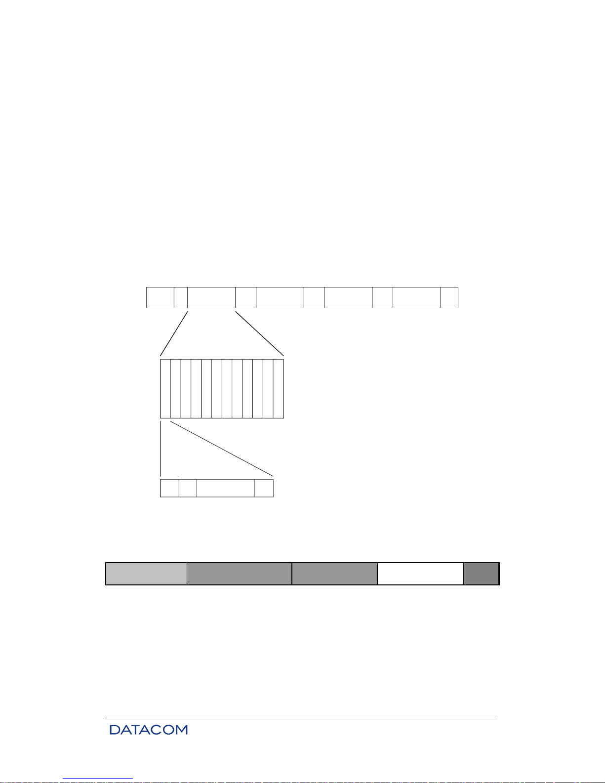
3.4.1. G.shdsl Frame Structure
The G.shdsl frame has four data blocks (payload blocks) that are separated by the header bits. The
header repeats itself each 6ms, regardless of the configured rate.
The header has an essential function for data transmission, for it ensures alignment, it transports
management information through EOC (Embedded Operations Channel) and it also has a data error
identification mechanism (CRC6).
The frame G.shdsl also allows to transmit CAS information (Channel Associated Signilling) from link E1.
. . .
O
H
O
H
O
H
O
H
TS
n
TS
1
TS
2
Stb
Sub-Block 1 Sub-Block 2 Sub-Block 3 Sub-Block 4 Sub-Block 5 Sub-Block 6 Sub-Block 7 Sub-Block 8 Sub-Block 9 Sub-Block 10 Sub-Block 11 Sub-Block 12
Frame
Sync
Payload
Block
Payload
Block
Payload
Block
Payload
Block
Payload Data, Bits 1
k
s
Figure 11. G.shdsl frame order diagram with CAS signaling
The sub block size varies according to the number of channels. Each sub block has Nx8 bits, where N is
the number of channels that was negotiated during handshake.
Timeslots E1 V.35 Nx64 kbit/s Ethernet Idle CAS
Figure 12. G.shdsl frame order diagram with CAS signaling
The frame structure that is sent and received by the G.shdsl modem consists in the E1 timeslots, in the
V.35 channel at Nx64k, in the Ethernet channel at Nx64kbit/s, in empty timeslots (idle) for filling the
installed modem rate and in a CAS timeslot, in this order.
Product Manual - DM991 Series V Family - 204.4092.08 18
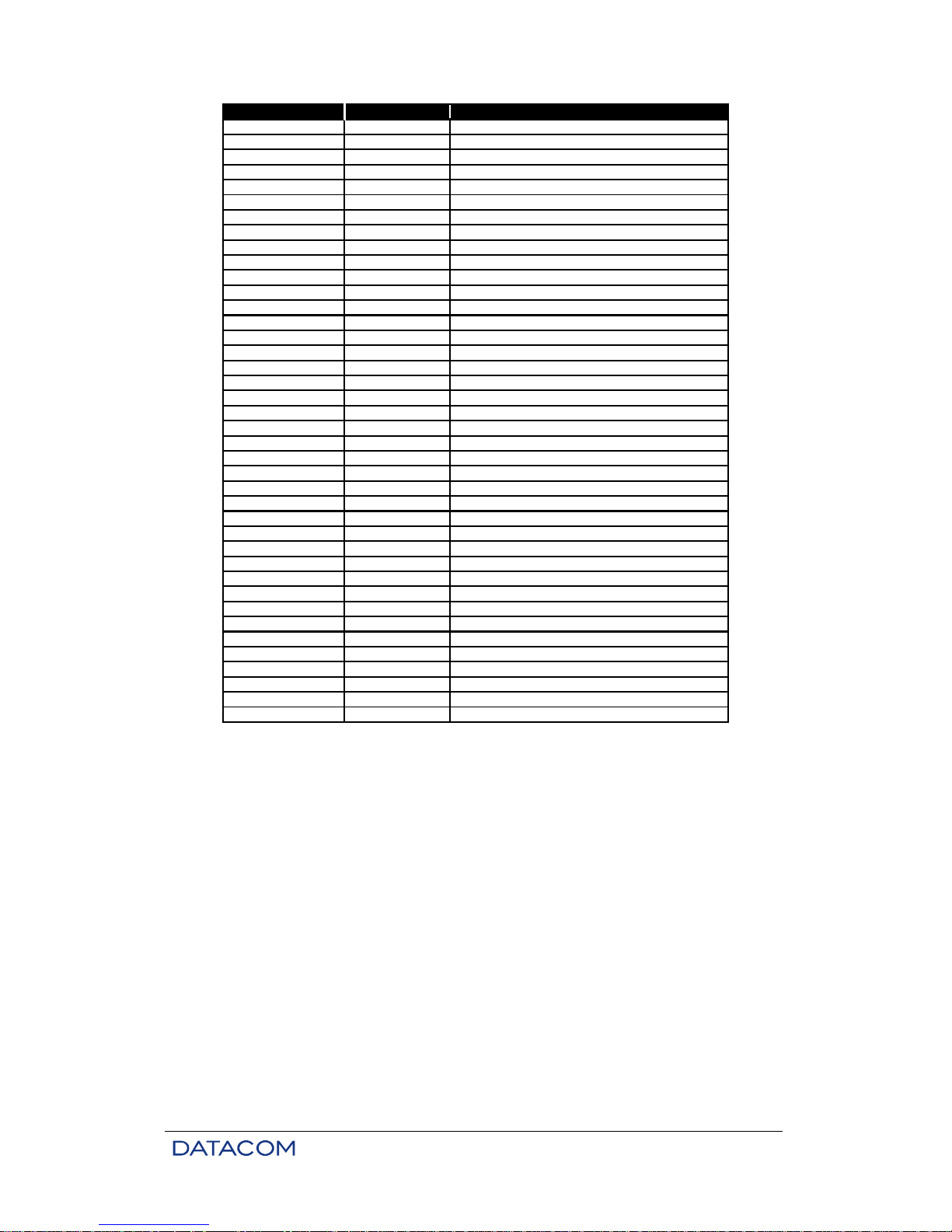
Bit
Name
Description
1-14 sw1-sw14 Frame Sync Word
15 fbit1/losd Fixed Indicator bit #1 (Loss of Signal)
16 fbit2/sega Fixed Indicator bit #2 (Segment Anomaly)
17 -> k+16 b1 Payload block #1
K + 17 eoc01 EOC bit #1
K + 18 eoc02 EOC bit #2
K + 19 eoc03 EOC bit #3
K + 20 eoc04 EOC bit #4
K + 21 crc1 Cyclic Redundancy Check #1
K + 22 crc2 Cyclic Redundancy Check #2
K + 23 fbit3/ps Fixed Indicator bit #3 (Power Status)
K + 24 sbid1 Stuff bit ID #1
K + 25 eoc05 EOC bit #5
K + 26 eoc06 EOC bit #6
k + 27 -> 2k + 26 b2 Payload block #2
2k + 27 eoc07 EOC bit #7
2k + 28 eoc08 EOC bit #8
2k + 29 eoc09 EOC bit #9
2k + 30 eoc10 EOC bit #10
2k + 31 crc3 Cyclic Redundancy Check #3
2k + 32 crc4 Cyclic Redundancy Check #4
2k + 33 fbit4/segd Fixed Indicator bit #4 (Segment Defect)
2k + 34 eoc11 EOC bit #11
2k + 35 eoc12 EOC bit #12
2k + 36 sbid2 Stuff bit ID #2
2k + 37 -> 3k + 36 b3 Payload block #3
3k + 37 eoc13 EOC bit #13
3k + 38 eoc14 EOC bit #14
3k + 39 eoc15 EOC bit #15
3k + 40 eoc16 EOC bit #16
3k + 41 crc5 Cyclic Redundancy Check #5
3k + 42 crc6 Cyclic Redundancy Check #6
3k + 43 eoc17 EOC bit #17
3k + 44 eoc18 EOC bit #18
3k + 45 eoc19 EOC bit #19
3k + 46 eoc20 EOC bit #20
3k + 47 -> 4k + 46 b4 Payload block #4
4k + 47 stb1 Stuff bit #1
4k + 48 stb2 Stuff bit #2
4k + 49 stb3 Stuff bit #3
Table 8. G.shdsl Frame Structure
During the data mode, link failures can occur. Such failures are monitored and reported to the user as
follows:
3.4.2. CRC Anomaly
A CRC anomaly shall be declared when the received CRC6 information is different from the CRC6
generated on the received data. The CRC6 bits are part of the previous G.shdsl frame. A discrepancy
between the received CRC6 value and the evaluated CRC6 on the interface indicates that an error
occurred in some bit (or bits) of the frame, but it does not indicate how many, or which bits were in error.
The interface status LED will blink once every second, remaining ON the most of the time while a CRC
error is showing up.
3.4.3. Loop Attenuation Defect
A loop attenuation defect occurs when the line displays an attenuation that exceeds the programmed
threshold. The standard limit for the DM991 G.shdsl interface is 35 dB.

Product Manual - DM991 Series V Family - 204.4092.08 19
3.4.4. SNR Margin Defect
An SNR margin defect occurs when the signal-to-noise ratio falls below the specified margin, i.e., when
the signal quality is too poor. The standard signal-to-noise ratio for the DM991 G.shdsl interface is 6 dB.
3.4.5. LOSW Defect
An LOSW (Loss of Sync Word Defect) defect shall be declared when at least three consecutive received
frames contain one or more errors in the framing bits. The term framing bits shall refer to that portion of
Frame Sync Word, Stuff Bits and Stuff Bit Ids – see Table 8 -, which are used for G.shdsl frame
synchronization. An LOSW defect shall be cleared when at least two consecutive received frames contain
no errors in the framing bits. For the DM991, the error indication is activated for one second after the
reception of the two error-free consecutive frames.
When the interface is indicating LOSWD, the DSL interface status LED blinks four times per second (4
Hz).
3.4.6. LOSW Failure
An LOSW failure (Loss of Sync Word Failure) shall be declared after 2.5 ± 0.5 seconds of contiguous
LOSW defect. The LOSWF shall be cleared when the LOSW defect is absent for 20 seconds or less (i.e.
clear within 20 s). The minimum hold time for indication of LOSW failure shall be 2 seconds.
When the interface is indicating LOSWF, the DSL interface status LED blinks eight times per second (i.e.
at 4 Hz).
3.5. G.shdsl Interface Configurations
The operation modes are all configured by software.
The explanation of the configuration parameters of the G.shdsl interface is presented below.
3.5.1. Terminal Type
Indicates if the interface operates as LTU (central office) or as NTU (subscriber).
When the modem is configured as LTU, it will determine every connection parameters during handshake,
as the Annex to be used, the number of channels, the clock type (synchronous or plesiochronous), etc. It
is not possible to recover the system clock from the interface clock when it is set up in such a way.
When the modem is set up as NTU, it is mandatory that the settings of the annex and of the clock type
(Frame Mode) be automatic, for it accepts any settings determined by the LTU.
It is not possible to interconnect two equipments which are set up for the same type of terminal, for the
handshake happens between LTU and NTU only.
3.5.2. Frame Mode
This option determines the interface operating mode as synchronous or plesiochronous.
In plesiochronous mode, the transmission and receive clocks are independent of the line clock, which is
generated by the LTU. The line clock shall be accurate to within ± 32 ppm of the nominal frequency, as
defined by G.991.2. Periodically, four stuff bits are automatically inserted to adequate the data clock to the
line clock. This procedure is essential for equipment synchronization.
Product Manual - DM991 Series V Family - 204.4092.08 20
When set up in synchronous mode, the line clock becomes the same as the data clock. The precision of
such clock gets to be, thus, the same as the precision of the clock that is selected as the equipment
synchronization clock. Recommendation G.991.2 states that the clock precision shall be within ± 32 ppm,
regardless of the clock scheme selected, so it is up to the user to set up a clock with such precision so as
to operate within the Recommendation bounds (or the user can use a less precise clock, operating out of
the Recommendation). In this way, the stb1 and stb2 stuff bits are always present, while stb3 and stb4 are
not transmitted.
In the automatic selection mode, the LTU will use the NTU-selected mode. If the NTU accepts any mode
(automatic configuration), the synchronous mode will be used.
3.5.3. Annex
The annexes determine slight variations on the Recommendation to better suit the equipment to the
employed line.
One of three annex options can be chosen: A, B or automatic selection.
Annex A describes those specifications that are unique to lines operating under conditions such as those
typically encountered within the North American network.
Annex B describes those specifications that are unique to lines operating under conditions such as those
typically encountered within European networks.
For the automatic selection mode, the LTU will employ the NTU-selected annex. If the NTU accepts any
type of annex, Annex B will be used.
3.6. Performance
The interface performance is directly related to the transmission line characteristics.
The gauge and the length of the line wire, the noise and the susceptibility to micro-interruptions to which
the line is subjected will determine the maximum transmission rate.
The range also diminishes if the line sports a great number of splices and stubs. The length of the stubs
also alters the line characteristics. This can increase the signal reflections and the line noise.
For a noise-free line using a 0.4-mm gage wire, with no seams or bifurcations, the range will be of 4,100
m for 2,304kbit/s, and with a modem set to 192kbit/s, the range can reach 7,100 m.
These tests were conducted with an artificial transmission line emulating the behavior of an actual line.
The table 9 includes the expected ranges for some rates on a noise-free artificial line.
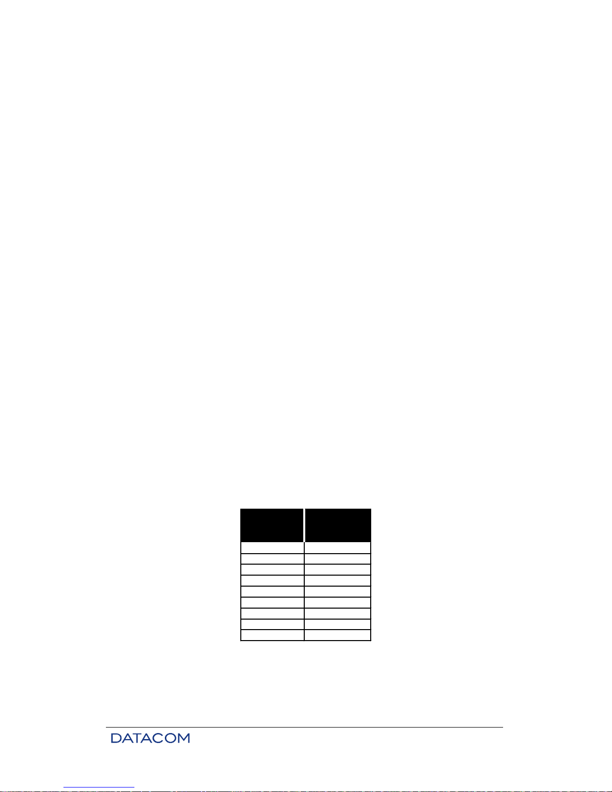
192 7,1
256 6,7
384 6,1
512 5,9
768 5,5
1024 5,1
1536 4,3
2048 4,2
2304 4,1
Data Rate
[kbit/s]
0.4mm Wire [km]
Table 9. G.shdsl Interface Reach
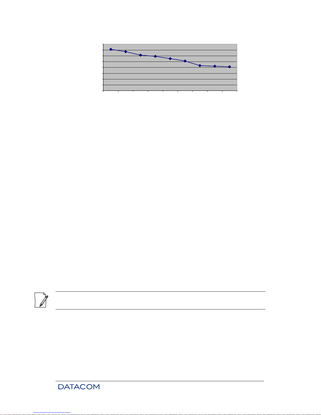
Product Manual - DM991 Series V Family - 204.4092.08 21
0
1000
2000
3000
4000
5000
6000
7000
8000
192 256 384 512 768 1024 1536 2048 2304
[kbit/s]
[m]
Figure 13. G.shdsl Interface Reach (m X kbit/s)
3.7. Four wire operation (4W)
The 4W modems presents two G.shdsl ports, these modems can operate in two ways.
3.7.1. Operating on two wires
When this modem is operating on 2 wires the data will be transmitted simultaneously on lines A and B,
adopting (1+1) protection system.
The protection is semi-automatic, that is, after commuting to the backup link, data passes through this link
until it has problems.
The switching time between both lines is approximately 1 second.
3.7.2. Operating on four wires:
When operating on 4 wires, this modem uses ports A and B as a single interface, being able to transmit
on a longer reach and more bandwidth.
The number of timeslots used in the 4 wires operation is always pair (Nx128kbit/s), that is, if the
configuration is set for an odd number, automatically one more timeslot will be used.
3.8. Electrical Protection
When the analogue lines of the G.shdsl interface pass through paths that can suffer from electric or
atmospheric discharges, it is recommended that the user adds primary protection devices to the lines.
The G.shdsl interface of models DM991C and DM991CE already has sparkler devices, among others, as
primary protection.
It is not appropriate to employ varistors as G.shdsl lines protection devices, as their high capacitance
value can lower the interface performance significantly. The same care should be taken when using
inductive protection.

Product Manual - DM991 Series V Family - 204.4092.08 22
4. V.35-V36/V.11 DIGITAL INTERFACE
The DB25 connector follows the ISO2110 Amd. 1 recommended pinout, for the V.35 interface as well as
for the V.36/V.11.
In the DM991S/SE modems, that pinout can be altered to the Telebrás standard through the straps.
Interface V.35
In the case of DM991S/SE modems, that pinning can be changed to the Telebrás standard through
straps.
In the case of DM991C/CE modems, you have the option of asking for equipment with a pinning
selections between ISO2110 Amd.1 and Telebrás standard through straps.
Data and clock signals are the differential balanced type, according to ITU-T’s V.11 recommendation.
Signals CT107, CT108, CT109, CT140, CT141 and CT142 follow the characteristics of recommendation
V.28 (compatible with recommendation V.10). Control signals CT105 and CT106 can be configured by
straps to follow the characteristics of recommendation V.28 (for V.35) or V.11 (for V.36/V.11).
The ETD can provide synchronism for data receiving through CT128.
The digital interface can be set up in rates from Nx64kbit/s to 2,304kbit/s on 2-wire modems (2W), and up
to 4,608kbit/s on 4-wire modems (4W).
Product Manual - DM991 Series V Family - 204.4092.08 23
DB25 M34 DB25†
ISO 2110
Amd. 1
ISO 2593
Telebrás
pinout
101 Protection ground P. Gnd 1 A 1
102 Signal ground S. Gnd 7 B 13
TDa 2 P 2
TDb 14 S 15
RDa 3 R 4
RDb 16 T 17
105 Request to send RTS 4 C 5 DM991
106 Ready to send CTS 5 D 7 DM991
107 Modem ready DSR 6 E 9 DM991
108 Terminal ready DTR 20 H 14 DTE
109‡ G.SHDSL interface synch DCD 8 F 10 DM991
XTCa 24 U 11
XTCb 11 W 24
TCa 15 Y 3
TCb 12 a/AA 16
RCa 17 V 6
RCb 8 X 19
ERCa 22 * 23
ERCb 23 * 8
140 Digital Remote Loopback Request RDL 21 N 12 DTE
141 Local Analogue Loopback request LAL 18 L 21 DTE
142 Test indicator TST 25 n/NN 25 DM991
CT Function Signal
Signal
source
113 DTE transmission clock DTE
114 Transmission clock DM991
103 Transmitted data DTE
104 Received data DM991
115 Reception clock DM991
128 External reception clock DTE
Table 10. V.35 Interface Pinout
† For DM991S/SE only (or optionally for DM991C/CE).
‡ On DM991C V.35-V.36/V.11 interfaces, the CT109 signal presents the aggregate state (G.shdsl),
remaining off while it is in error condition (except when there is CRC error).
* For ISO2110 Amd. 1, the ERCa (22) and ERCb (23) pins do not correspond to the CT128.
Product Manual - DM991 Series V Family - 204.4092.08 24
DB25 DB37 DB25†
ISO 2110
Amd. 1
ISO 4902
Telebrás
pinout
101 Protection ground P. Gnd 1 1 1
102 Signal ground S. Gnd 7 19 13
TDa 2 4 2
TDb 14 22 15
RDa 3 6 4
RDb 16 24 17
RTSa 4 7 5
RTSb 19 25 18
CTSa 5 9 7
CTSb 13 27 20
107 Modem ready DSR 6 11 9 DM991
108 Terminal ready DTR 20 12 14 DTE
DCDa 8 13 10
DCDb 10 31 22
XTCa 24 17 11
XTCb 11 35 24
TCa 15 5 3
TCb 12 23 16
RCa 17 8 6
RCb 9 26 19
ERCa 22 * 21
ERCb 23 * 25
140 Digital Remote Loopback Request RDL 21 14 23 DTE
141 Local Analogue Loopback request LAL 18 10 8 DTE
142 Test indicator TST 25 18 12 DM991
114 Transmission clock DM991
CT Function Signal
Signal
source
109‡ G.SHDSL interface synch DM991
113 DTE transmission clock DTE
105 Request to send DTE
106 Ready to send DM991
103 Transmitted data DTE
104 Received data DM991
115 Reception clock DM991
128 External reception clock DTE
Table 11. V.35 Interface Pinout
† For DM991S/SE only (or optionally for DM991C/CE).
‡ On DM991C V.35-V.36/V.11 interfaces, the CT109 signal presents the aggregate state (G.shdsl),
remaining off while it is in error condition (except when there is CRC error).
* For ISO2110 Amd. 1, the ERCa (22) and ERCb (23) pins do not correspond to the CT128.
Product Manual - DM991 Series V Family - 204.4092.08 25
5. G.703 - G.704 INTERFACE
The interface allows usage of coaxial cable (75ohms) or for twisted pairs (120ohms). The cables are
attached through transformers, so there is no polarity for the twisted pair.
5.1. DM991S/SE
There are straps which allow connecting the external net of the coaxial cable to the ground cable. This
works either for the input channel (RX-IN) as for the output channel (TX-OUT).
The output wire that goes through pin 18B of the EDGE 2x30 connector is connected to the central pin of
the E10 strap, and is the TX-OUT cable, that can be connected to the ground cable through this strap. In
this case, it must be identified for each cabinet model which was the TX-OUT screw to be grounded by the
strap, so it can be connected to the coaxial cable net. On the sub-racks, usually, the inferior TX-OUT
screw is grounded.
The input wire that goes through pin 21B of the EDGE 2x30 connector is connected to the central pin
through strap E11, and is the RX-IN cable, that can be connected to the ground wire through this strap.
The same identification procedure of which screw has been grounded must take effect in this case. In the
sub-rack, usually, the inferior TX-OUT screw is grounded.
Modem signal G.703 is available on Dial Backup terminals in the terminal strip.
Function Signal
screw connector
block
Signal source
Received data OUT core BkpC DM991
Received data OUT shield BkpD DM991
Transmitted data IN core BkpA E1 Network
Transmitted data IN shield BkpB E1 Network
Table 12. DM991S/SE - Pinout in the G.703 Screw connector block.
Function Signal DB25 Signal source
Received data OUT core 4 DM991
Received data OUT shield 17 DM991
Transmitted data IN core 2 E1 Network
Transmitted data IN shield 15 E1 Network
Table 13. DM991S/SE - G.703 Telebrás (DB25) Standard Pinout
When using twisted pair (120ohms), make sure the straps are not in the ground position.
When installing the DM991S/SE
, remove the protection varistors from the cabinet or sub rack. These
varistors deform the G.703 signal pulses, which can cause wro
ng bits, working intermittently, or even
completely stopping the circuit activation.
In case the cabinet or shelf was made by DATACOM or has
gas-filled valve arrester instead of varistors, no changes are required.
Product Manual - DM991 Series V Family - 204.4092.08 26
Function Signal DB25 Signal Source
Received data OUT core 21 DM991
Received data OUT shield 14 DM991
Transmitted data IN core 18 E1 Network
Transmitted data IN shield 25 E1 Network
Table 14. DM991S/SE - G.703 Proprietary Pinout (DB25)
5.2. DM991C/CE
There are straps that allow you to connect the external coaxial cable network to the ground. On models
DM991C/CE with PCI rev. 04 or higher, this applies both to the input channel (RX-IN) and to the output
channel (TX-OUT). On models DM991C/CE with PCI rev. 03 or lower, this applies only to the input
channel (RX-IN); in this case, the external output coaxial cable network (TX-OUT) is always connected to
the ground.
The G.703 signal output is available on the BNC OUT connector or between the pins 4 and 5 of the RJ48.
The G.703 signal input is available on the BNC IN connector or between the pins 1 and 2 of the RJ48
Function Signal RJ45 Signal Source
Received data OUT 4 DM991
Received data OUT 5 DM991
Transmitted data IN 1 E1 Network
Transmitted data IN 2 E1 Network
Table 15. DM991C/CE - G.703 RJ48 Pinout
Be careful as not to let those straps be in the grounded position when a 120-
ohm twisted pair is used on
the RJ48.

Product Manual - DM991 Series V Family - 204.4092.08 27
6. ETHERNET INTERFACE
The DM991SE and DM991CE Ethernet interfaces allow interconnecting two LANs thru G.shdsl
aggregated. It can be configured to Nx64kbit/s speed, to the aggregate configured limit. This tributary can
be used joined with other modem tributaries.
Accepts packets of up to 1552 bytes, supporting VLAN.
6.1. Ethernet physical level
The DM991CE and DM991SE converters Ethernet interface is 10/100BaseT, according to the IEEE 802.3
specification.
The connection to the Ethernet interface is done through an RJ45 connector, seen in the front panel. The
connector pinout is such that allows the use of straight cables to connect the equipment to Ethernet hubs.
6.2. Remote Bridge
The bridge’s basic function is to segment a local network, avoiding all the Ethernet traffic to be transmitted
by the local equipment to the remote equipment, wasting band.
To do so, the bridge can automatically learn the MAC addresses of the stations connected to the local
network. In that way, it can filter the network traffic and transmit to the WAN side only the packets
corresponding to the MAC addresses that do not pertain to the local network, besides broadcast and
multicast packets.
The bridge operates on the MAC level of the Ethernet interface. In this way the tributary is completely
transparent for upper layers protocols, such as TCP/IP, UDP, etc.
The bridge local address table can store up to 1.000 MAC addresses. If a station remains inactive for
more than five minutes, its address will be removed from the table.
The process of filtering the packets to be transmitted imposes no limitation to the data flow. The delay
introduced by the Bridge processing is of only 1 Ethernet frame.
The bridge has a buffer to Ethernet -> G.shdsl that may store up 322 packages Ethernet with 1552 bytes,
but smaller packages may be stored in greater quantity.
In order G.shdsl -> Ethernet has a buffer of 64 packets of 1552 bytes Ethernet. Similarly, using smaller
packages permites store more ones. Using this direction there is no filtering, because it has already been
done by the bridge from remote equipment.
6.3. Ethernet Interface Configurations
The following interface configurations are possible:
• WAN Speed - It allows for the selection from 1 to 36 64-kbit/s time slots on 2-wire
modems (2W), and from 1 to 72 time slots on 4-wire modems (4W);
• Self-negotiation - allows negotiation with the equipment connected by the Ethernet
interface on the operating mode, interface velocity, and flow control use;
• Duplex - it is possible to choose between the Full-Duplex (both sides transmit
simultaneously) and Half-Duplex modes (one side transmits at a time);
 Loading...