


NET-AIO11 User’s Manual (Rev 1.0)
-1- http://www.daqsystem.com
NET-AIO11
User’s Manual
Windows, Windows2000, Windows NT, Windows XP, Windows 7 and Windows CE are trademarks of Microsoft. We
acknowledge that the trademarks or service names of all other organizations mentioned in this document as their own property.
Information furnished by DAQ system is believed to be accurate and reliable. However, no responsibility is assumed by DAQ
system for its use, nor for any infringements of patents or other rights of third parties which may result from its use. No license is
granted by implication or otherwise under any patent or copyrights of DAQ system.
The information in this document is subject to change without notice and no part of this document may be copied or
reproduced without the prior written consent.
Copyrights 2011-2012 DAQ System Co., LTD. All rights reserved.

NET-AIO11 User’s Manual (Rev 1.0)
-2- http://www.daqsystem.com
Contents
1. Introduction
2. Product Features
3. Hardware Device
4. Software
References
(Caution)
★ The board and external input/output signals of the device have
to connect the common ground(Frame) to protect the board and
peripheral devices.
★ The board operates in a safe location, in a clean environment.
★ External connection is completed before board power
connection, the function should be run by the rated power.

NET-AIO11 User’s Manual (Rev 1.0)
-3- http://www.daqsystem.com
1. Introduction
NET-AIO11 is the High function Signal Processing board to support Analog Input and
Digital Output. The 8-channel A / D converted data by applying TI TMS320C55xx DSP
chip analog signal can be obtained the high speed data via USB 2.0 interface and Ethernet
interface.
The device can be used to support the power over Ethernet cable(UTP). There are no
separate power devices because the power is supported through the Injector or
PoE(Power over Ethernet) Hub.
1.1 Function
- 8-Ch 16-Bit Sigma-Delta ADC
- Isolated Digital Input/Output
- USB 2.0 FS Interface
- 10/100Mbps Ethernet TCP/IP Interface
- PoE(Power over Ethernet) PD(Power Device) Circuit
1.2 Internal Block Diagram
DSP
TMS320C55xx
ADC FPGA
Analog
8-Channel
Gain
Control
Digital
Input /Output
ETH
Controller
Ethernet
Link
USB Interface
[Figure 1. Internal Block Diagram]
1.3 Operation Mode
1.3.1 Continuous Mode
Continuous Mode, is that continuously collect the data from board. Setting the
Sampling Rate by selected Interface (USB/NET) is collecting the data continuously.
1.3.2 Delay Mode
Delay Mode, via set the Sampling Rate after a certain time, is that total 524,288(512k)
data store in the memory, and read the data when the user want.
NET-AIO11 User’s Manual (Rev 1.0)
-4- http://www.daqsystem.com
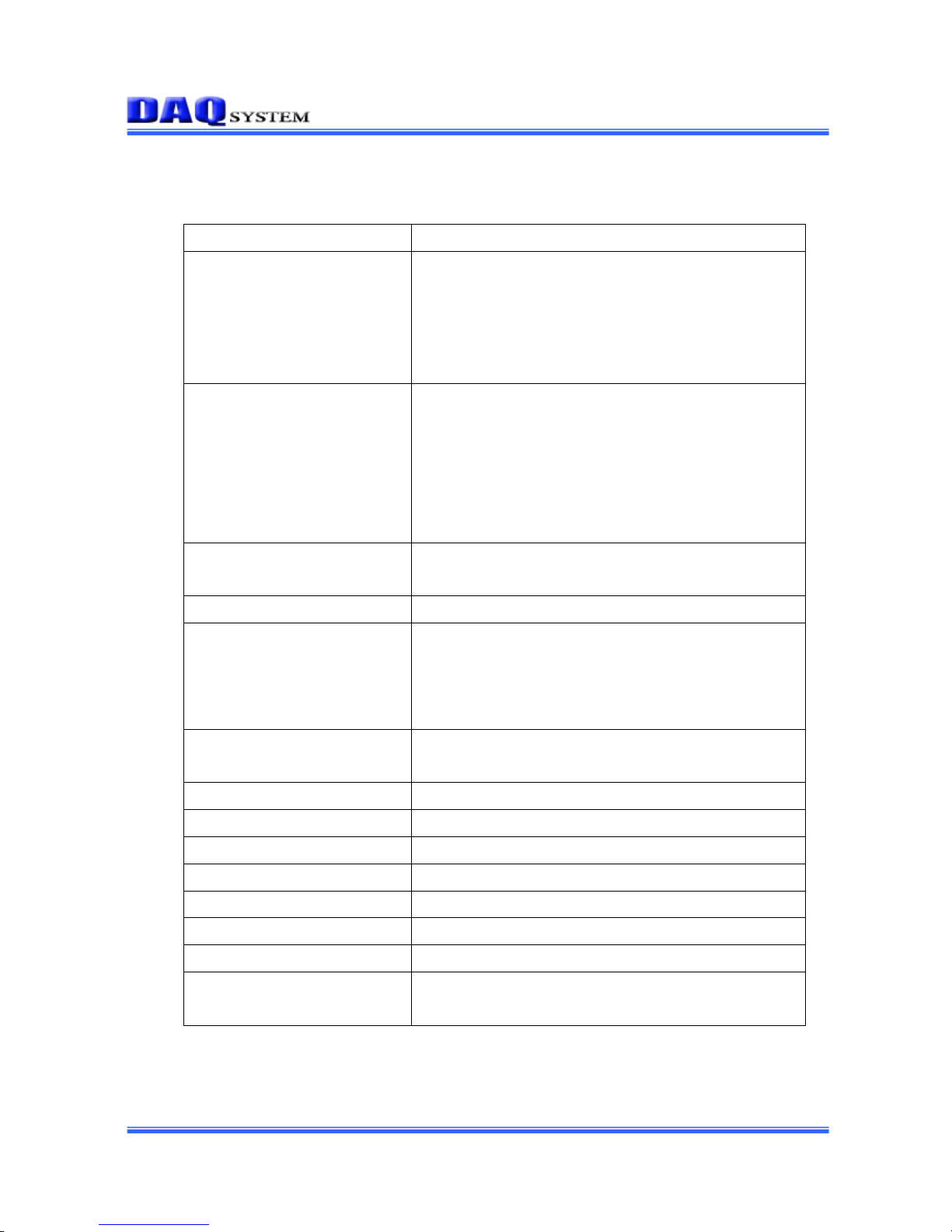
2. Product Features
[Table 1. NET-AIO11 Specification]
List
Specification
Interface
USB B-type Connector
RJ-45 Ethernet Connector
Header Pin Connector for Analog Input
Header Pin Connector for Digital Input/Output
5VDC Power Connector
Analog Input(ADC)
Channel : 8
Maximum Input Range : ±10V
Resolution : 16-bit
Maximum Sampling :
Ethernet 32,768 Sample/sec
USB 16,384 Sample/sec
Digital Input/Output
Channel : 8 Inputs, 8 Outputs
Input/Output Signal Level : 12/24VDC, Isolated
USB
USB 2.0 Full Speed(12Mbps)
Ethernet
10/100Mbps
Auto cable detection
Can be set Board Network Information (etc. IP)
Support only fixed IP
DSP
TI TMS320C55xx
On-chip USB 2.0
Option
PoE PD
Size
160x100mm
Operation Temperature
Operation Moisture
Power
5VDC±5%, 600~800mA
Support S/W
Kernel mode WDM Driver/User mode DLL
Support OS
Windows 2K/XP/7 32-bit
Component
NET-AIO11 Board, Install CD(include Sample
Program)

NET-AIO11 User’s Manual (Rev 1.0)
-5- http://www.daqsystem.com
3. Hardware Device
In this chapter, board jumper set and connector for interfaced the PC or other operation
equipment is described.
USB-B
Connector
LED
(PWR,RUN)
POWER
Connector
Ethernet
Connector
AIN
Connector
DSP Mode
Setup Jumper
Reset Switch
[Figure 2. Connector, Switch Placement]
3.1 DSP Mode Setup Jumper (J2)
The execution mode of the board is the USB boot mode and flash boot mode. The Flash
boot mode (jumper OFF) is the general board operation. On the other hand, the USB boot
mode is used when frequent firmware updates or develops flash memory program.
3.2 USB-B Connector (CN1)
It is a B-type USB connector. It is connected to a PC and is done a data transmission.
3.3 LED(PWR, RUN) (D22)
The power and status of board is displayed. When connecting the power, the red led
light on. When collecting the data, the green led light on.

NET-AIO11 User’s Manual (Rev 1.0)
-6- http://www.daqsystem.com
3.4 AIN(Analog Signal Input) Connector (J7)
Analog input signals are received an input the range of ± 10V differential (Differential)
signal and a single (Single-ended) signals. In a single signal, an AINxN pin connects to the
Ground of input signal, an AINxP pin connects to the input signal.
3
876 254
1
9
1413121110
15
2019181716
J7
BOX HEADER RA 2x13, 2.54mm
242322
21
25
26
[Table 2. AIN Connector Description]
Pin No.
Pin Name
Description
Remark
1
AGND
Analog Ground, GROUND
2
AIN1P
Analog Input CH1, Positive
3
AIN1N
Analog Input CH1, Negative
4
AGND
Analog Ground, GROUND
5
AIN2P
Analog Input CH2, Positive
6
AIN2N
Analog Input CH2, Negative
7
AGND
Analog Ground, GROUND
8
AIN3P
Analog Input CH3, Positive
9
AIN3N
Analog Input CH3, Negative
10
AGND
Analog Ground, GROUND
11
AIN4P
Analog Input CH4, Positive
12
AIN4N
Analog Input CH4, Negative
13
AGND
Analog Ground, GROUND
14
AIN5P
Analog Input CH5, Positive
15
AIN5N
Analog Input CH5, Negative
16
AGND
Analog Ground, GROUND
17
AIN6P
Analog Input CH6, Positive
18
AIN6N
Analog Input CH6, Negative
19
AGND
Analog Ground, GROUND
20
AIN7P
Analog Input CH7, Positive
21
AIN7N
Analog Input CH7, Negative
22
AGND
Analog Ground, GROUND
23
AIN8P
Analog Input CH8, Positive
24
AIN8N
Analog Input CH8, Negative
25
AGND
Analog Ground, GROUND
26
AGND
Analog Ground, GROUND
NET-AIO11 User’s Manual (Rev 1.0)
-7- http://www.daqsystem.com
3.5 Ethernet Connector (J11)
It connects to the Ethernet Hub or Ethernet Adapter. It automatically is detected
Cross/Direct cable.
3.6 POWER Connector (J6)
It is a power of the board, input over +5VDC, 1A.
J6
DC-JACK, 2mm
1
2
PCB
[Table 3. POWER Connector Description]
Pin No.
Pin Name
Description
Remark
1
+5VDC
Power 5V
2
GND
Power Ground
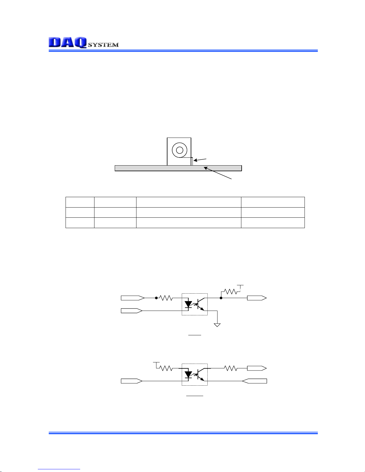
3.7 Digital Signal Input/Output Connector (J13)
It connects to each 8-bit Digital Input/Output signals. The isolated 12/24VDC signals can
be input or output. The circuit is as [Figure 3].
DIN_COM
DINx
BINx
+3.3V
BOUTx
DOUT0
+3.3V
22
330
2.4K
DOUT_COM
Input
Output
[Figure 3. Digital Input/Output Circuit]

NET-AIO11 User’s Manual (Rev 1.0)
-8- http://www.daqsystem.com
3
876 254
1
9
1413121110
15
2019181716
J13
BOX HEADER RA 2x10, 2.54mm
[Table4. Digital Signal Output Connector Description]
Pin No.
Pin Name
Description
Remark
1
DIN_COM
Digital Input Common Terminal,
2
DOUT_COM
Digital Output
3
DIN0
Digital Input 0
4
DOUT0
Digital Output 0
5
DIN1
Digital Input 1
6
DOUT1
Digital Output 1
7
DIN2
Digital Input 2
8
DOUT2
Digital Output 2
9
DIN3
Digital Input 3
10
DOUT3
Digital Output 3
11
DIN4
Digital Input 4
12
DOUT4
Digital Output 4
13
DIN5
Digital Input 5
14
DOUT5
Digital Output 5
15
DIN6
Digital Input 6
16
DOUT6
Digital Output 6
17
DIN7
Digital Input 7
18
DOUT7
Digital Output 7
19
EGND
External Ground, External Ground
20
+12V
External Input Power
+12VDC

NET-AIO11 User’s Manual (Rev 1.0)
-9- http://www.daqsystem.com
4. Software
NET-AIO11 board can easily access many of the features of the library (API) to
implement, and the sample program is provided to the user.
4.1 Sample Program
The library is used to implement the sample program, it is organized as follows.
1
2
3
6
7 8
9
10
11
12
13
14 15
16
17
18
19
20
21
22
23
25 26
27
30
31 32
4 5
24
28 29
[Figure 4. Sample Program]
4.1.1 Program Description
[Table 5. Sample Program Function Description]
No.
Control
Function
1
DAQ RUN
Board Initialization and continuous mode data collection run.
2
Interface Select
Select the interface to connect host (PC). USB/Ethernet.
3
IP
It is an Ethernet IP of the board for TCP/IP connection.
4
Port Number
It is a port number to use TCP/IP connection.
5
Port Number
It is a port number that was obtained on the board by “SEL”
command. 6 SEL
Execute the host interface connection.
7
Data Level
Collected Data for the selected channel is converted to a voltage
level. 8 Graph Channel
Select the channel to display the section 7.
9
Store to Lib
It displays that the number of bytes of received data from the

NET-AIO11 User’s Manual (Rev 1.0)
-10- http://www.daqsystem.com
Read from Lib
board.
It displays that the number of data bytes of read from the library
buffer in application.
10
Buffering WR Pointer
Buffering RD Pointer
It displays a saving pointer of library buffer.
It displays a reading pointer of library buffer.
11
View Scale
A scaling factor displays on the graph.
12
Offset
It is an offset to set the up/down position of graph.
13
Set
View Scale and Offset is applied to the graph.
14
Sample Rate
It selects an Analog data sampling rate.
15
Set
It sets the Sampling rate.
16
0x
It enters the digital output value.
17
Digital Out
It sets the digital output value.
18
Digital In
It confirms the Digital Input value.
Displayed Data, the value of low 0~7 bits are a DIN value, and
8~11 bits value are setup value of DIP switch.
19
IP Address
It enters an IP address to be stored the board.
20
MAC Address
It enters a MAC information to be stored the board.
21
SUB-NET MASK
It enters a MASKING information to be stored the board.
22
GATE WAY
It enters an address of Network Gateway to be stored the board.
23
Port Number
It enters a port numbers to be stored the board.
24
PROGRAM
The section of 20~24 saves in the flash memory.
The stored data will be reflected in the firmware when the board
is reset. Be careful of the confliction to set the same information.
This function is only available with the USB interface, so No. 2)
"USB" selection and this function can use when the No. 6) “SEL”
run.
25
sec
It enters a delay time of Delay Mode Data collection.
26
Delay + Store
After a delay time of Delay Mode, it executes a data collection.
27
Data READ
It reads a data that is collected in the Delay Mode.
When you run it that is not the end of delay and data collection,
the Beep sound occurs. Otherwise, the data is displayed on the
right side of the graph.
28
RAM LOAD
At right in the path of the editor, USB booting binary loads the
device. First, the running mode should be selected as the USB.
29
FIND
It searches the USB load image.
30
FIND EMIF.BIN
It searches an execution image to be stored in the flash memory.

NET-AIO11 User’s Manual (Rev 1.0)
-11- http://www.daqsystem.com
31
FLASH LOAD
Searched File image is loaded into the board memory.
Run 2~3 times more.
32
FLASH PROGRAM
Saved an image saves into the flash memory.

NET-AIO11 User’s Manual (Rev 1.0)
-12- http://www.daqsystem.com
References
1. USB 2.0 System Architecture
-- Don Anderson, USB SIG(www.usb.org)
2. Universal Serial Bus Specification
-- Compaq/Intel/Microsoft/NEC, MindShare Inc. (Addison Wesley)
3. AN201 How to build application using API
-- DAQ system
4. AN342 NET-AIO11 API Programming
--DAQ system
 Loading...