

Page 1

VXI-SC-1102 User Manual
32-Channel Multiplexer Amplifier Module
February 1997 Edition
Part Number 321385A-01
© Copyright 1997 National Instruments Corporation. All Rights Reserved.
Page 2
Internet Support
support@natinst.com
E-mail: info@natinst.com
FTP Site: ftp.natinst.com
Web Address: http://www.natinst.com
Bulletin Board Support
BBS United States: (512) 794 -5422
BBS United Kingdom: 01635 551422
BBS France: 01 48 65 15 5 9
Fax-on-Demand Support
(512) 418-1111
Telephone Support (U.S.)
Tel: (512) 795-8248
Fax: (512) 794-5678
International Offices
Australia 03 9879 5166, Austria 0662 45 79 90 0, Belgium 02 757 00 20,
Canada (Ontario) 905 785 0085, Canada (Québec ) 514 694 8521, Denmark 45 76 26 00,
Finland 09 527 2321, France 01 48 14 24 24, Ger many 089 741 31 30, H on g Kong 264 5 3186,
Israel 03 5734815, Italy 02 413091, Japan 03 5472 2970, K orea 02 596 7456,
Mexico 5 520 2635, Netherlands 0348 433466, Nor w ay 32 84 84 00, Singapore 22658 86,
Spain 91 640 0085, Sweden 08 730 49 70, Switzerland 056 200 51 51, Taiwan 02 377 1200,
U.K. 01635 523545
National Instruments Corporate Headquarters
6504 Bridge Point Parkw ay Austin, TX 78730-503 9 Tel: (512) 794-0100
Page 3

Important Information
Warranty
The VXI-SC-1102 is warranted agai nst defects in mater ials and workm anshi p fo r a period of one year from the date
of shipment, as evidenced by receipts or other documentation. National Instruments will, at its option, repair or replace
equipment that proves to be defective during the warranty per iod. This warrant y includes par ts and labor .
The media on which you receive National Instru ments software ar e warranted not to fail to execute pro grammi ng
instructions, due to defects in materials and workmanship, for a period of 90 days from date of shipment, as evidenced
by receipts or other documentation. National Instruments will, at its option, repair or replace software media that do
not execute programming instructions if National Instruments receives notice of such defects during the warranty
period. National Instruments does not warr ant that t he operatio n of the softwar e shall be uni nte rrupt ed or erro r free.
A Return Material Authorization (RMA) number must be obtained from the factory and clearly marked on the outside
of the package before any equipment will be accepted for warranty work. Natio nal Instrum ents wil l pay the shippin g
costs of returning to the owner par ts whi ch are cov ered by w arranty .
National Instruments believes that the information in this manual is accurate. The document has been carefully
reviewed for technical accuracy. In the event that technical or typographical errors exist, National Instruments reserves
the right to make changes to subsequent editi ons of this document without prior notice to holders of this edition. The
reader should consult National Instruments if errors are suspected. In no event shall National Instruments be liable for
any damages arising out of or related to this docum ent or the in format ion contai ned in it.
E
XCEPT AS SPECIFIED HEREIN
SPECIFICALLY DISCLAIMS ANY WARRANTY OF MERCHANTABILITY OR FITNESS FOR A PARTICULAR PURPOSE
C
USTOMER’S RIGHT TO RECOVER DAMAGES CAUSED BY FAULT OR NEGLIGENCE ON THE PART OF NATIONAL
I
NSTRUMENTS SHALL BE LIMITED TO THE AMOUNT THERETOFORE PAID BY THE CUSTOMER
WILL NOT BE LIABLE FOR DAMAGES RESULTING FROM LOSS OF DATA, PROFITS, USE OF PRODUCTS, OR INCIDENTAL OR
CONSEQUENTIAL DAMAGES, EVEN IF ADVISED OF THE POSSIBILITY THEREOF
Instruments will apply regardless of the form of action, whether in contract or tort, including negligence. Any action
against National Instruments must be brought within one year after the cause of action accrues. National Instruments
shall not be liable for any delay in performan ce due to causes beyo nd it s reasonable cont rol. The warranty pr ovided
herein does not cover damages, defects, malf unctio ns, or s ervice fai lures caused by owne r’s fail ure to fol low the
National Instruments in sta llat ion, o perat ion, or ma inte na nce instr uct ions; owner ’s modif icat ion of the p roduct;
owner’s abuse, misuse, or negligent acts; and power failure or surges, fire, flood, accident, actions of third parties, or
other events outside reasonable control.
, N
ATIONAL INSTRUMENTS MAKES NO WARRANTIES, EXPRESS OR IMPLIED, AND
.
. N
ATIONAL INSTRUMENTS
. This limitatio n of the li abil ity of Natio nal
Copyright
Under the copyright laws, this publication may not be reproduced or transmitted in any form, electronic or mechanical,
including photocopying, reco rding, storin g in an in format ion retr iev al system , or tra nslati ng, in wh ole or in par t,
without the prior written consent of Nation al Inst rument s Corpo ration .
Trademarks
LabVIEW®, NI-DAQ®, RTSI®, ComponentWorks™, CVI™, Measure™, SCXI™, and VirtualBench™ are
trademarks of Nationa l Ins trumen ts C orpor atio n.
Product and company names listed are trademarks or trade names of their respective companies.
WARNING REGARDING MEDICAL AND CLINICAL USE OF NATIONAL INSTRUMENTS PRODUCTS
National Instruments products are not design ed with comp onents and testing in tend ed to ensure a level o f reliabi lity
suitable for use in treatment and diag nosi s of humans . Appli cations of Nationa l Inst rument s prod ucts inv olving
medical or clinical treatment can create a potential for accidental injury caused by product failure, or by err ors on the
part of the user or application designer. Any use or applicati on of Nati onal Instrum ents pr oducts for or involvin g
medical or clinical treatment must be performed by properly trained and qualified medical personnel, and all traditional
medical safeguards, equipment, and procedures that are appropriate in the particular situation to prevent serious injury
or death should always continue to be used when National Instruments products are being used. National Instruments
products are NOT intended to be a substitute f or any for m of establ ished pr ocess, proce dure, or equi pmen t used to
monitor or safegua rd huma n he alth and sa fety in med ical or clin ical t reat ment .
Page 4

About This Manual
Organization of This Manual................................................ ...... ..... .............................ix
Conventions Used in This Manual................................................................................x
National Instruments Documentation.............................. ..... .................................. ......xi
Customer Communication............................................................................................xi
Chapter 1
Introduction
About the VXI-SC-1102...............................................................................................1-2
What You Need to Get Started.....................................................................................1-3
Software Programming Choices...................................................................................1-3
National Instruments Application Software...................................................1-3
NI-DAQ Driver Software...............................................................................1-4
VXIplug&play Instrument Driver..................................................................1-5
Optional Equipment......................................................................................................1-6
Unpacking.....................................................................................................................1-6
Table
of
Contents
Chapter 2
Installation
Current-Loop Receivers................................................................................................2-3
Installing Your Hardware .............................................................................................2-4
Chapter 3
Signal Connections
Front Connector............................................................................................................3-1
Signal Descriptions......................................................................................... 3-3
Channel Input Signal Connections.................................................................3-3
Ground-Referencing Your Signals...................................................3-4
Cold-Junction Sensor Connection..................................................................3-6
© National Instruments Corporation v VXI-SC-1102 User Manual
Page 5

Table of Contents
Chapter 4
Theory of Operation
Functional Overview....................................................................................................4-1
VXIbus Interface.......................................................................................................... 4-2
Digital Control Circuitry.............................................................................................. 4-2
Analog Circuitry........................................................................................................... 4-3
Analog Input Channels...................................................................................4-3
Analog Output................................................................................................ 4-3
Chapter 5
Calibration
Calibration Equipment Requirements................................................. .........................5-1
Gain and Offset Calibration................................................................. ...... ...... ............. 5-2
Sample Program for Calibration...................................................................................5-4
Appendix A
Specifications
Appendix B
Customer Communication
Glossary
Index
Figures
Figure 1-1. VXI Signal Conditioning System.......................................................... 1-1
Figure 1-2. The Relationship between the Programming Environment, Your
Instrument Driver, and Your VXI-DAQ Hardware .............................. 1-5
Figure 2-1. VXI-SC-1102 Parts Locator Diagram...................................................2-2
Figure 2-2. Bent and Trimmed Resistor................................................................... 2-3
Figure 3-1. VXI-SC-1102 Front Connector Pin Assignments................................. 3-2
Figure 3-2. Ground-Referenced Signal Connection.................................................3-5
Figure 3-3. Floating Signal Connection Referenced to Chassis Ground................. 3-6
VXI-SC-1102 User Manual vi © National Instruments Corporation
Page 6

Tables
Table of Contents
Figure 4-1. VXI-SC-1102 Block Diagram...............................................................4-1
Figure 5-1. Analog Bus Receptacle Pin Assignment ...............................................5-2
Table 3-1. Front Connector Signal Descriptions.....................................................3-3
© National Instruments Corporation vii VXI-SC-1102 User Manual
Page 7

This manual des cribe s the el ectri cal an d mech an ical a spect s of the
VXI-SC-1102 and contains informat io n concerning its installation and
operation. The VXI-SC-1102 is a signal conditioning submodule in the
VXI-data acquisition (VXI-DAQ) line of National Instruments
products. The VXI-SC-1102 is designed for signa l conditionin g of
thermocouples, volt and m illivolt sour c es, and 4 to 2 0 mA source s o r
0 to 20 mA pr ocess- c urren t sou rc es. T he V XI- SC-1 102 has 32
differential analog input channels and one cold-junction sensor channel.
Organization of This Manual
The VXI-SC-1102 U se r Ma nual is organized as follows:
• Chapter 1, Introduction, d escribe s th e V XI-SC -11 02, lists wha t
you need to get started, optional software and optional e quipment,
and explains how to u npac k th e V XI-SC- 110 2.
• Chapter 2, Installation, describes how to install cu rrent- loop
receivers on your VXI-SC-1102 and gives inform ation about
installing your VXI-SC-1102 submodule into the VXI -SC-1000
carrier module.
• Chapter 3, Signal Connections, de scribes the input signal
connections to the VXI-S C-1102 sub module via the front
connector.
• Chapter 4, Theory of Operation, contains a functional overview of
the VXI-SC-1102 and e xpl ains the op era tion o f each func tional
unit.
• Chapter 5, Calibration, discusses the ca libration procedures for the
VXI-SC-1102.
• Appendix A, Specifications, lists the specifications for the
VXI-SC-1102.
• Appendix B, Customer Communication, co ntains form s y ou ca n
use to request help from National Instruments or to comment on our
products.
About
This
Manual
©
National Instruments Corporation ix VXI-SC-1102 User Manual
Page 8

About This Manual
•The Glossary contains an alphabetical list and description of terms
used in this manual, including abbreviations, acronym s, metric
prefixes, mnemonics, symbols, an d general data acqu isition terms.
•The Index contains a n alpha betica l list o f ke y term s and topic s in
this manual, including the page whe re you can fin d ea ch on e.
Conventions Used in This Manual
The following conventions are used in this manual.
< > Angle brackets containing numbers separated by an ellipsis represent a
range of values assoc iated wit h a port, bit, or signal nam e (for exam ple,
ACH<0..7> stands for the signals ACH0 through ACH7).
bold italic Bold italic text denotes a note, caution, or warning.
italic Italic text denotes emphasis, a cross reference, or an introduction to a
key concept.
monospace Denotes text or characters that are to be literally input from the
keyboard, sections of c ode, p rogra mmin g exa m ples, a nd synt ax
examples. This fo nt is also use d for the prope r n ame s of d isk d rive s,
paths, directories, pro gra ms , subp rog rams, su bro utines, de vice n ames ,
functions, variables, filenames, and extensions, and for statements and
comments taken from program code.
PC Refers to the IBM PC/XT, the IBM PC AT, and compatible computers.
VXI-MIO module Refers to any of the N ationa l Instrum ents V XI- MIO Se ries of p lug-in
data acquisition boards.
carrier module Refers to the VXI-SC-1000, which plugs directly into a VXI slot and on
which VXI-SC submodules are installed.
VXI-SC submodule Refers to VXI signal conditioning hardware that installs onto the carrier
module.
Abbreviations, acronyms, me tric prefixes, mnemonics, symbols, an d
terms are listed in the Glossary.
VXI-SC-1102 User Manual x
©
National Instruments Corporation
Page 9

National Instruments Documentation
The VXI-SC-1102 U se r Ma nual is one piece of the documenta tion set
for your VXI-DAQ s ystem . You co uld have any of seve ral type s of
documents, depending on the h ardw are and sof tware in yo ur syste m.
Use the different types of docu me nts you ha ve a s follow s:
• Your VXI-DAQ hardware user manuals—These manuals have
detailed information about the VXI-DAQ hardware that plugs into
or is connected to yo ur V XIbu s c hassis. Us e thes e ma nuals f or
hardware installation and configuration instructions, specification
information about your VXI-DAQ hardware, and application hints.
• Software documentation—You may have both application software
and driver software documentation. National Instruments
application software incl udes Com ponen tW ork s, LabV IEW,
LabWindows
Instruments driver software includes NI-DAQ and VXIplug&play
instrument drivers. After you set up y our ha rdw are system, use
either your application or driver softw are docume ntation to help
you write your application. I f you ha ve a lar ge, c omplica te d
system, it is worthwhile to look thr ough the software
documentation befo re yo u co nfigu re y our hard w are.
• Accessory installation guides or manuals—I f you are using
accessory products, read the terminal block and cable assembly
installation guides or accessory board user manuals. They explain
how to physically co nnec t the releva nt p ieces of the s ystem .
Consult these guides when you are mak ing your c onne ctions.
®
/CVI, Measure, and VirtualBench. National
About This Manual
Customer Communication
National Instruments wants to rece ive you r com ments o n ou r prod ucts
and manuals. We are interested in the applications you develop with our
products, and we want to help if you have problems with them. To make
it easy for you to contact us, this manual contains comment and
configuration forms for you to complete. These for ms are in
Appendix B, Customer Communication, at the end of this manual.
©
National Instruments Corporation xi VXI-SC-1102 User Manual
Page 10
Chapter
Introduction
This chapter describe s the VX I-SC -1102, lists wha t y ou need to get
started, optional soft w are and option al eq ui p m en t , an d explains ho w to
unpack the VXI-SC-1102.
The VXI-SC-1102 is part of the VXI signal conditioning system, which
consists of a carrier m odu le and o ne or m ore V XI sign al con ditioning
submodules or filler panels as shown in Figure 1-1.
2
1
4
3
5
To VXIbus
Chassis
6
8
1
9
1 Analog Bus Receptacle
2SCMPs
3 SCMP Socket
©
National Instruments Corporation 1-13 VXI-SC-1102 User Manual
4 Address Switch
5 VXI-SC Subslot 1
6 VXI-SC Subslot 2
Figure 1-1.
7 VXI-SC Carrier Module
8 VXI-SC-1150 Submodule
9 VXI-SC Submodule
VXI Signal Conditioning System
7
Page 11

Chapter 1 Introduction
The VXI-SC-1000 is a carrier module that installs into a slot in a
VXIbus chassis and is po pulated w ith one or tw o submod ules. T he
VXI-SC-1102 is a submodule that installs into VXI-SC subslots on a
VXI-SC-1000 carrier module.
Your VXI-SC-1000 ca rrier modu le is shipp ed w ith a filler pane l
installed in one of the submodule sites. This filler panel is necessary for
the attachment of the front panel, so you should leave it in place until
you are ready to install a VXI-SC submodule.
About the VXI-SC-1102
The VXI-SC-1102 is a submodule for the signal conditio ning of
thermocouples, low-bandwidth volt and millivolt sources, 4 to 20 mA
current sources, a nd 0 to 2 0 mA p roce ss-curr en t sourc es . The
VXI-SC-1102 has 32 diffe rential analog inp ut cha nnels a nd o ne
cold-junction sensor channel. On each channel, the VXI-SC-1102 has a
three-pole lowpass filter with a 2 Hz cutoff frequency to reject 60 Hz
noise. Each channel also has an amplifier with a selectable gain of 1 or
100. You can multiplex the VXI-SC-1102 inputs to a single output,
which drives a single V XI-MIO boa rd c hanne l.
The VXI-SC-1102 operates with full functionality with National
Instruments VXI-MIO modules. You can multiplex several
VXI-SC-1102 submodules an d oth er VX I signa l con ditioning
submodules into a single channel on the VXI-MIO module, greatly
increasing the number of analog input signals that you can digitize.
You can also use National Instruments terminal blocks, which have
screw terminals to which you attach the input signals for the
VXI-SC-1102. In addition, some of these terminal blocks have a
temperature sensor for thermocouple cold-junction compensation
(CJC). The VXI-SC-1102 multiplexes this cold-junction sensor with the
32 input channels during a h ardw are sc an . A N ational Instr uments
isothermal terminal block is recommende d for thermoc ouple
applications.
Detailed specifications of the VXI-SC-1102 ar e listed in Appendix A,
Specifications.
VXI-SC-1102 User Manual 1-14
©
National Instruments Corporation
Page 12

What You Need to Get Started
To set up and use y our VXI- SC-1 102 , you w ill need the follow ing
items:
❑ VXI-SC-1102 submodule
VXI-SC-1102 User Ma nua l
❑
❑ VXI-SC-1000 carrier module and documentation
❑ VXI-MIO module and documentation
❑ One of the following software packages and documentation:
ComponentWorks
LabVIEW for Windows
LabWindows/CVI fo r W indo ws
NI-DAQ for PC compatibles
VirtualBen ch
VXIplug&play instrumen t dr iver
Chapter 1 Introduction
❑ Your VXIbus system
Software Programming Choices
There are several op tions to choo se from whe n programm ing your
National Instruments VXI-DAQ hardw are. You c an use LabVIE W,
LabWindows/CVI, Comp one ntWorks, V irtu alBench, or o ther
application development enviro nments with eith er NI-DAQ or the
VXIplug&play instrument driver. Both NI-DAQ and the
VXIplug&play instrument driver access the VXI-DAQ hardware
through the VISA driver software.
National Instruments Application Software
LabVIEW features interactive graphics, a state-of-the-art user
interface, and a po werf ul g raphic al progr am ming langua ge. The
LabVIEW Data Acquisition VI L ibra r y, a se ries of V Is fo r using
LabVIEW with National Instruments DAQ hardware, is included with
LabVIEW. The LabVIEW D ata A cquisitio n VI Libr ar y is functiona lly
equivalent to the NI-DAQ software.
©
National Instruments Corporation 1-15 VXI-SC-1102 User Manual
Page 13

Chapter 1 Introduction
LabWindows/CVI features interactive graphics, a state-of-the-art user
interface, and uses th e ANSI standa rd C pr ogr am ming la nguage . The
LabWindows/CVI Data Ac quisition Lib rary, a se ries of fun ctions f or
using LabWindows/CVI with National Instruments DAQ hardware, is
included with the NI-DAQ software kit. The LabWindow s/CVI Data
Acquisition Library is functionally equivalent to the NI-D AQ sof twar e.
ComponentWorks con tains tools for data acq uisition and instr ument
control built on NI-DAQ driver softw are. Component Works provide s a
higher-level programming interface for building virtual instruments
through standard OLE controls and DLLs. With ComponentWorks, you
can use all of the configuration tools, resource management utilities,
and interactive control utilities included with NI-DAQ.
VirtualBench features VIs that combine DAQ products, software, and
your computer to create a standalone instrument with the added benefit
of the processing, display, and storage capabilities of your computer.
VirtualBench instruments lo ad and sa ve wav efor m data to disk in the
same forms that can be us ed in po pular sp readsh eet pr ogram s and wor d
processors.
Using LabVIEW, Lab Windo ws/C VI , Compon en tW ork s, or
VirtualBench software will greatly reduce the development time for
your data acquisition and control application.
NI-DAQ Driver Software
The NI-DAQ driver sof tware is included at no ch ar ge with all National
Instruments DAQ hardware. NI-DAQ is not packaged with accessory
products. NI-DAQ has an extensive library of functions that you can
call from your application progr amming environment. The s e functions
include routines for analog input (A/D conversion), buffered data
acquisition (high-speed A/ D c onver sion) , analog ou tput ( D/A
conversion), waveform generation, digital I/O, counter/timer
operations, SCXI, RTSI, self-calibration, messaging, and acquiring
data to extended memory.
NI-DAQ has both high-level DAQ I/O functions for maximum ease of
use and low-level DAQ I/O functions for maximum flexibility and
performance. Ex am ples of h igh- leve l func tions are stre aming data to
disk or acquiring a certain number of data po ints. An examp le of a
low-level function is writing directly to registers on the DAQ device.
NI-DAQ does not sacrifice the performance of National Instruments
VXI-SC-1102 User Manual 1-16
©
National Instruments Corporation
Page 14
VXI
plug&play
Chapter 1 Introduction
DAQ devices because it lets multiple devices operate at their peak
performance.
NI-DAQ maintains a consistent software interface among its different
versions so that you can cha nge p latfo rms w ith minimal mo dific ations
to your code.
Instrument Driver
National Instruments distributes VXIplug&play instrument drivers free
of charge. VXIplug&play instrument drivers are one leve l above the
NI-DAQ device driver and contain high-lev el software function s whose
architecture is specified by the VXIplug&play Systems Alliance. The
VXIplug&play standards increase interoperability with other vendors,
and ensure that drivers are designed and presented in a consistent
fashion that facilitates ease of use. Refer to Figure 1-2 to see the
relationship between your software components.
ComponentWorks,
LabVIEW, LabWindows/CVI,
or VirtualBench
Figure 1-2.
The Relationship between the Programming Environment, Your
Instrument Driver, and Your VXI-DAQ Hardware
Other Application
Development Environments
VXI
plug&play
Instrument Driver
NI-DAQ Driver Software
VISA
VXI-DAQ Hardware
©
National Instruments Corporation 1-17 VXI-SC-1102 User Manual
Page 15

Chapter 1 Introduction
Optional Equipment
National Instruments offers a v ari ety of pr oducts to u se with your
VXI-SC-1102 module, as follows:
• Terminal blocks and 96-pin cables that allow you to attach input
signals to your submodule
• SCXI Process Current Resistor Kit
For more specific information about these products, refer to your
National Instruments catalogue or c all the of fice near est you .
Unpacking
Your VXI-SC-1102 subm odule is sh ippe d in a n antistatic p acka ge to
prevent electrostatic damage to the submodule. Electrostatic discharge
can damage severa l com pon ents on the su bm odu le. To a vo id su ch
damage in handling the submodule, take the following prec autions.
• Ground yourself via a ground ing strap or by holdin g a grounded
object.
• Touch the antistatic package to a me tal part of your VXIbus chassis
before removing the su bmo dule from th e pa ck ag e.
• Remove the submodule from the package and inspect the
submodule for loose components or any othe r sign of damage .
Notify National Instruments if the module appears damaged in any
way. Do not install a damaged submodule into your VXIbus
chassis.
• Never touch the exposed pins of connectors.
VXI-SC-1102 User Manual 1-18
©
National Instruments Corporation
Page 16

Chapter
Installation
2
This chapter describes how to install current-loop receivers on your
VXI-SC-1102 and gives information abou t installing your
VXI-SC-1102 submodu le into the VXI -SC-1000 c arrie r mod ule .
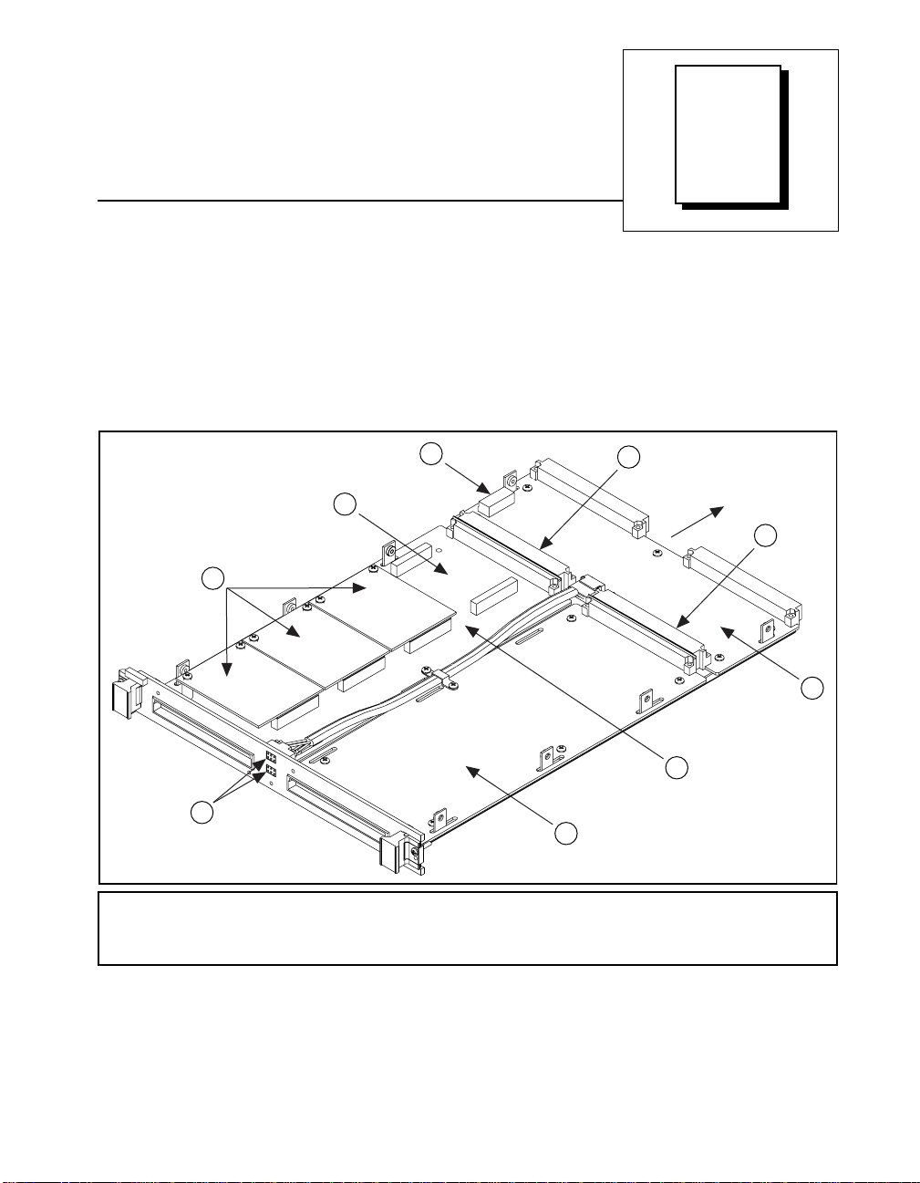
Refer to Figu re 2-1, VXI -SC-11 02 Parts Locator Di agram, for
information as you read the instructions in this chapter.
©
National Instruments Corporation 2-19 VXI-SC-1102 User Manual
Page 17

Chapter 2 Installation
2
3
1
4
1 Serial Number 2 Product Name 3 Assembly Number 4RCLx Pads
©
VXI-SC-1102 User Manual 2-20
National Instruments Corporation
Page 18

Current-Loop Receivers
The VXI-SC-1102 has pads fo r tran sforming ind ividua l cha nnels to
current-to-vo ltage co nvert ers. Na tional Instr umen ts offers an SCXI
Process Current Resistor Kit of four 249 Ω, 0.1%, 5 ppm, 1/4 W
resistors. The reference designators for the cu rrent loop resistors have
the following format: for input channel x, the resistor is RCLx. For
example, the resistor for chann el 28 is RCL28.
Warning: Before installing the resistors in your submodule, make sure that there are
no signals connected to your submodule front connector.
Install the resistors by performing the following steps:
1. Follow the instructions in the VXI-SC-1000 Carrier Module
Installation Guide to remove the VXI-SC-1102 submodu le from
the carrier assembly.
2. Bend and trim the resistor lead as shown in Figure 2-2. Be sure that
the resistor does no t extend more th an 0.6 5 in. ab ove the su rfac e of
the circuit board.
Chapter 2 Installation
Figure 2-1. VXI-SC-1102 Parts Locator Diagram
Figure 2-2. Bent and Trimmed Resistor
3. Insert the resistor into the appropriate pad, labeled RCLx.
4. Solder the leads to the pad on the bottom side of the module.
5. Follow the instructions in the VXI-SC-1000 Carrier Module
Installation Guide to replace the VXI-SC-1102 submod ule in the
carrier assembly.
©
National Instruments Corporation 2-21 VXI-SC-1102 User Manual
Page 19

Chapter 2 Installation
Installing Your Hardware
Follow the instructions in the VXI-SC-1000 Carrier Module Installation
Guide to replace the VXI-SC-110 2 submo dule and to install th e
assembled VXI-SC carrier module in the VXIbus chassis.
VXI-SC-1102 User Manual 2-22
©
National Instruments Corporation
Page 20

Chapter
Signal Connections
This chapter describes the analog input signal connections to the
VXI-SC-1102 submodule via the front connecto r.
Caution:
!
Front Connector
Static electricity is a major cause of comp onent failure. To pre vent damage
to the electrical components in the module, observe antistatic techniques
whenever removing a module from the chassis or whenever working on a
module.
Figure 3-1 sh ows the pin assign ments f or the VX I-SC-1 102 front
connector.
3
©
National Instruments Corporation 3-23 VXI-SC-1102 User Manual
Page 21

Chapter 3 Signal Connections
CGND
NC
NC
NC
NC
NC
NC
NC
CGND
NC
NC
NC
NC
NC
NC
NC
CGND
NC
NC
NC
NC
NC
NC
NC
NC
NC
NC
CGND
CJSENSOR
CJSENSOR
CGND
+5 V
32
31
30
29
28
27
26
25
24
23
22
21
20
19
18
17
16
15
14
13
12
11
10
A
CH0CH1CH2CH3CH4CH5CH6CH7CH8CH9-
CH10-
CH11-
CH12CH13CH14-
CH15-
CH16CH17CH18CH19CH20CH21CH22-
9
8
7
6
5
4
3
2
1
CH23CH24CH25CH26CH27CH28CH29CH30CH31-
32
31
30
29
28
27
26
25
24
23
22
21
20
19
18
17
16
15
14
13
12
11
10
B
CH0+
CH1+
CH2+
CH3+
CH4+
CH5+
CH6+
CH7+
CH8+
CH9+
CH10+
CH11+
CH12+
CH13+
CH14+
CH15+
CH16+
CH17+
CH18+
CH19+
CH20+
CH21+
CH22+
9
8
7
6
5
4
3
2
1
CH23+
CH24+
CH25+
CH26+
CH27+
CH28+
CH29+
CH30+
CH31+
C
32
31
30
29
28
27
26
25
24
23
22
21
20
19
18
17
16
15
14
13
12
11
10
9
8
7
6
5
4
3
2
1
Figure 3-1. VXI-SC-1102 Front Connector Pin Assignments
VXI-SC-1102 User Manual 3-24
©
National Instruments Corporation
Page 22

Signal Descriptions
Chapter 3 Signal Connections
Table 3-1.
Pin Signal Name Description
A1 +5 V +5 VDC Source—Powers the
A2, A5, A16,
A24, A32
A3, A4 CJSENSOR Cold-Junction Temperature
B1–B32 CH31-
C1–C32 CH31+
All other pins are not connected.
Front Connector Signal Descriptions
temperature sensor on the terminal
block. 0.2 mA of source not
protected.
CGND Chassis Ground—Tied to the
VXIbus chassis.
Sensor Input—Connects to the
temperature sensor of the terminal
block.
Negative Input Channels 31–0
through
CH0-
through
CH0+
—Negative side of differential
input channels.
Positive Input Channels 31–0
—Positive side of differential
input channels.
Channel Input Signal Connections
The signal terminals for the positive input channels are located in
column C of the connector. The signal terminal for each corresponding
negative input channel is locat ed in column B of the connector . Each
input goes to a separate filte r and a mplifier that is m ultiplexed to the
module output buffer. Th e ter mina l b lock tempe ratur e sensor
output—connected to p ins A 3 and A4 (CJSE NSOR) —is al so fi ltere d
and multiplexed to the module output buffer.
The differential input sign al range of a VX I-SC-11 02 input ch annel is
±10 V/G, where G is the gain selec ted on the VXI-SC-1 102 input
channel. Th is di ff er en tia l i np ut r an ge is th e ma ximu m me asu ra bl e
voltage difference between the positive and negative channel inputs.
The common-mode input signal range of a VXI-SC-1102 input channel
©
National Instruments Corporation 3-25 VXI-SC-1102 User Manual
Page 23

Chapter 3 Signal Connections
Warning: Exceeding the input damage leve l (±42 VAC peak or VD C be tween inp ut
!
channels and chassis ground) can damage the VXI-SC-110 2, the VXIbus,
and the VXI-MIO module. National Instruments is
injuries resulting from such signal connections.
Applying a voltage greater than ±42 VAC peak or VDC to the VXI-SC-1102
is an electrical shock hazard. National Instruments is
damages or injuries resulting from suc h voltage a pplication.
Note: Exceeding the differential or common-mode input channel ranges results
in a distorted signal measurement.
is ±11 V. This common-mode input range for either positive or negative
channel input is the maximum input voltage (relative to CGND) that
will result in a valid measurement. Each channel includes input
protection circuitry to withstand the accidental application of voltages
up to ±42 VA C peak or VD C.
NOT
liable for any
NOT
liable for any
Ground-Referencing Your Signals
Your input signals can be e ith er g rou nd-re fe renc ed, as sho wn in
Figure 3-2, or floating, as s how n in Figure 3-3. B efore y ou c onnec t
your thermocouple or any other signal, de termine wh ether it is
floating or ground-referen ce d. I f it is a f loating sign al, yo u m ust
ground-reference the sig nal in one o f two w ays. You ca n conne ct the
negative channel input to chassis ground as shown in Figure 3-3 or you
can use the clamping resistors on a VXI-TB Series terminal block. The
VXI-TB Series terminal block may also have a resistor pack for pulling
up the positive inputs for open-thermocouple detec tion. Consult the
terminal block installation guide for d etails.
Do not ground signals w hich ar e alr eady gr oun d-ref ere nced; doin g so
will result in a ground loop, which adversely affects your measurement
accuracy.
VXI-SC-1102 User Manual 3-26
©
National Instruments Corporation
Page 24

Chapter 3 Signal Connections
CH0 +
CH0 -
+
V
diff
-
+
V
cm
-
CH1 +
CH1 -
Connector
Front Signal
+
-
+
-
VXI-SC-1102
Figure 3-2. Ground-Referenced Signal Connection
©
National Instruments Corporation 3-27 VXI-SC-1102 User Manual
Page 25

Chapter 3 Signal Connections
CH0 +
CH0 -
Floating
Signal
Make this connection to
ground reference the signal.
+
V
s
-
Reference to
Chassis Ground
CH1 +
CH1 -
Front Signal
CGND
Figure 3-3. Floating Signal Connection Referenced to Chassis Ground
Cold-Junction Sensor Connection
Pins A3 and A4 (CJSENSOR) connect the temperature sensor located
on the National Instruments VXI-T B Series term inal block to the
VXI-SC-1102. The CJSENSOR signal is measured relative to CGND.
Pins A3 and A4 are connected within the VXI-SC-1102 so the position
of the MTEMP/DTEMP switch on the VX I-TB Series ter minal block
does not matter. The input is overvoltage-protected to 15 VDC with the
power on and off.
+
-
+
-
Connector
VXI-SC-1102
Warning: Exceeding the overvoltage protection on the CJSENSOR input can damage
!
the VXI-SC-1102, the VXIbus, and the VX I-M IO bo ard. N ational
NOT
Instruments is
liable for any damages or injuries resulting from such
signal connections.
VXI-SC-1102 User Manual 3-28
©
National Instruments Corporation
Page 26

Chapter
Theory of Operation
This chapter contains a function al overview of the VXI-SC -1102 an d
explains the operation o f ea ch f unctiona l unit.
Functional Overview
The block diagram in Figure 4-1 illustrates the key functional
components of the VXI-SC-1102.
CH 0 +
CH 0 –
+
Inst.
Amp
–
Input Protection
and Lowpass Filter
Gain 0
Lowpass
Filter
Buffer
4
Buffer
Mux
32-to-1 Mux
CH 31+
CH 31 –
Front Signal Connector
CJSENSOR
©
National Instruments Corporation 4-29 VXI-SC-1102 User Manual
+
Inst.
Amp
–
Input Protection
and Lowpass Filter
Input Protection
and Lowpass Filter
Gain 31
Lowpass
Filter
Lowpass
Filter
Buffer
Buffer
Figure 4-1.
Switch
Switch
Gain
Register
Calibration EEPROM
Digital
Control
VXI-SC-1102 Block Diagram
Analog Bus +
Analog Bus -
Connector to Carrier Module
Page 27

Chapter 4 Theory of Operation
The major components of the VXI-SC -1102 are a s follows:
• VXIbus interface
• Digital control circuitry
• Analog circuitry
The VXI-SC-1102 consists of 32 multiplexed input channels, each with
a software-progra mmab le gain of 1 or 100. E ach inpu t cha nnel ha s its
own lowpass filter with a cutoff frequency of 2 Hz. The V XI-SC-110 2
also has digital control circuitry for automatic control of channel
scanning, temperature sen sor se lect ion, a nd gain sele ction .
VXIbus Interface
The VXI-DAQ module controls the VXI-SC-1102 over the VXIbus.
The VXI-SC-1000 carrier module serves as an interface from the
VXI-SC-1102 to the VXIbus.
Digital Control Circuitry
The digital control c ircu itry co nsists of the ad dress handle r and the
following registers: Module ID, Configuration, Status, EEPROM, Gain,
and Channel. The address ha ndler controls w hich register is being
addressed. The Module ID Register contains the module ID 42 decimal,
a code unique to the VX I-S C-1102 . The Conf igur ation Re giste r
configures the VXI -SC-110 2 f or the d esired scan ning mo de a nd
connection to the rear signal connector. The Status Register indicates
whether the input channels have settled after a change in the gains. The
EEPROM Register is the addr ess for inte rf acing with the subm odule ’s
EEPROM, which contains calibration information. The Gain Register
selects between gain s of 1 o r 1 00 fo r e ach o f the 32 ch anne ls . The
Channel Register selects a channel for a single measurement or a start
channel for a sca n. Ref er to Software Programming Choices in
Chapter 1, Introduction, of this manual to learn about options fo r
programming the control circuitry.
VXI-SC-1102 User Manual 4-30
©
National Instruments Corporation
Page 28

Analog Circuitry
The analog circuitry per ch anne l consists of a lowpass fi lter and an
amplifier with a software -sele ctable gain of 1 or 100 . The C JSEN SO R
channel also has a buffered low pass filter but has no amp lifier. The
channels and CJSENSOR are multiplexed to a single output buffer.
Analog Input Channels
Each of the 32 analog input channels dr iv es a sepa ra te amp lifier with a
programmable gain of 1 or 100. Th en the signal passes thr ough a
three-pole lowpass filter with a cutoff frequency of 2 Hz.
Note: Because of the 2 Hz bandwidth of the input channels, you must wait
approximately 3 s after changing the gains before the channels settle and
you can take an accurate measurement. NI-DAQ au tomatically reads the
Status Register to determine when the module output has settled.
The temperature sensor consists of a thermistor located on a National
Instruments VXI terminal block. The tempera tur e sen sor is for
cold-junction compensation of thermocouples. The CJSENSOR
channel also passes through a 2 Hz lowpass filter to reject unwa nted
noise. Along with the other 32 input channels, the CJSENSO R is
multiplexed to the output buffer, where it can be read by the VXI-MIO
module.
Chapter 4 Theory of Operation
For a measurement accurac y of 0.0 12% of fu ll scale, th e minimum scan
interval is 3 µs. This is the smallest interval in which you can switch
between analog channels on the submodule and still measure accurate
voltages. The 3 µs scan interval gives you a maximum sampling rate of
333 kHz. Because each VXI-SC-1102 channel contains a 2 Hz lowpass
filter, the 333 kHz sample rate allows you to sample multiple channels
without undersampling any c hann el.
Analog Output
The 32 input channels and the CJSENSOR are multiplexed into one
output. This output is passed to the VXI-SC-1000 carrier module, where
it is connected to the Analog Bus for measurement by a VXI-MIO
module.
©
National Instruments Corporation 4-31 VXI-SC-1102 User Manual
Page 29

Chapter
Calibration
This chapter di scusses th e calib ratio n pr oced ures fo r the VXI-SC -110 2.
Using the procedure described in this chapter , you will be able to
calculate the gain error and voltage offset on a per channel per gain
basis. You can store these constants in the onboard EEPROM for future
use and for automatic calibra tion when you are using National
Instruments software. The V XI-SC -11 02 come s f rom the fa ctor y with
factory-determined calibration constants in the EEPROM. However,
National Instruments recomme nd s that y ou reca librate your
VXI-SC-1102 at least once per year or when you operate the submodule
outside the 20° to 30° C temperature range. If you are not using National
Instruments software to store the calibration data in the EEPROM, refe r
to the VXI-SC-1102 Reg ister- Lev el Pro gramme r Ma nual for a more
detailed description of the EEPROM.
In order to calibrate the VXI-SC-1102, you will need to apply precision
voltages to the channel inputs and/or ground the channel inputs.
Calibration Equipment Requirements
5
According to standard practice, the equipment you use to calibrate the
VXI-SC-1102 should be 10 times as accurate as the VXI-SC-11 02.
Calibration equipment with four times the accuracy of the
VXI-SC-1102 is generally considered acceptable. To calibrate the
VXI-SC-1102, you need a voltmeter with the following specifications:
• Accuracy ±6 ppm sta ndar d readin g
±15 ppm sufficient reading
• Range ±10 V
• Resolution 8.5 digits
A multiranging 8.5-digit digital multimeter (DMM) can perform the
necessary calibrations.
To make sure that the DMM does not introduce an additional offset, you
can determine the offset error of the DMM by shorting its leads together
©
National Instruments Corporation 5-33 VXI-SC-1102 User Manual
Page 30

Chapter 5 Calibration
and reading t h e meas ure d va lu e. T his valu e, t he DM M o ffs et , mu s t be
subtracted from all subseq uent m easur eme nts.
Measure the submodule’ s output at the analog bus rece ptacle (se e
Figure 1-1 for the location of this receptacle). Refer to Figure 5-1 to
connect the positive DMM input to MUX+ and the negative DMM input to
MUX-.
MUX+ MUX- CAL- CAL+
MUX- MUX+ CAL+ CAL-
Figure 5-1. Analog Bus Receptacle Pin Assignment
Gain and Offset Calibration
To determine the of fse t a nd ga in ca libra tion f act ors o f th e
VXI-SC-1102 for a g iven gain, per for m th e follo wing ste ps for a
two-point calibration. For two-point calibration, it is best to use input
voltages that correspond to the signal range of interest. For example, to
measure bipolar v oltages over the subm odule’s fu ll input rang e, choose
-9.9 V/G (negative full-scale) and +9.9 V/G (positive full-scale) as your
two input voltages.
1. Se lec t the desir ed channel. Set the channel gain to the desired gain.
2. Apply the input for the first calibration point. To select negative
full scale as the calibration point, apply -9.9 V/G for an input
voltage.
a. Apply the input voltage to the channel selected in Step 1.
VXI-SC-1102 User Manual 5-34
©
National Instruments Corporation
Page 31

Chapter 5 Calibration
Note: To make one of your calibration points the zero point, connect the positive
and negative channel leads to one of the chassis ground pins on the front
connector or terminal block.
b. Measure the input voltage with the DMM. Call the measured
voltage input1.
Note: If you are using a calibrator that supplies accurate voltages, you can
simply use the known applied voltage for
input1
instead of measuring.
c. Measure the mo dule o utput at the a nalog bus rece pta cle wit h
the DMM. Call the measured voltage
output1
.
3. Repeat Step 2, applying the input for the seco nd calibra tion p oint.
Call the measured voltages
input2
and
output2
. To select
positive full scale as the calibration point, repeat Step 2 and apply
+9.9 V/G.
4. You now have two pairs of voltages (
(
input2, output2
). Each pair consists of an input voltage and an
input1, output1
) and
output voltage.
5. Convert the output vo ltages from volt un its to you r VX I-M IO
module binary unit. You must take into consideration the polarity
of your VXI-MIO module, its resolution (12 bi ts or 16 bits), and
gain. For example, if you are using the 12-bit VXI-MIO-64E-1 in
bipolar mode with the gain set to G
, your output voltage s f or
MIO
the autozeroing option will be represented in binary units as given
by the following formula:
Binary
=
Output
-----------------5 V
12
G
•
•
2
MIO
For other VXI-MIO modules, refer to the user manual to determine
the appropriate formula.
6. You now have a new set of pairs referred to as voltage binary pairs
(
input1, bin_output1
pairs to the
SCXI_Cal_Constants
) and (
input2, bin_output2
function or VI as described in
). Pass these
your software us er do cu me ntation .
Note: When you use 0 V and positive full-scale for your two calibration points,
you elimin ate t he e rro r a t 0 V an d at p os it ive f ull - sca le vo lta g e. H ow e ver ,
because of nonlinearity, the error at the negative full-scale voltage will be
two times the nonlinearity error. This is also true for the positive full-scale
voltage if you use the negative full-scale voltage and 0 V as your two
calibration points.
©
National Instruments Corporation 5-35 VXI-SC-1102 User Manual
Page 32

Chapter 5 Calibration
When you make a me asurem ent us ing L abV IEW, C omp onentWo rks, or
VirtualBench, the driver automatically uses the calibration constants to
correct the measured voltages.
When you use application development environments other than
LabVIEW, ComponentWorks, or VirtualBench, you have the option to
apply the calibration constants to measured voltages through the NI-DAQ
API.
Sample Program for Calibration
The following sample C program will help you calibrate the
VXI-SC-1102. The calibration constants are stored only in NI-DAQ
memory. The (input, o utput) vo ltage pair s read by a DMM must be
entered by hand. Before this program is run, the NI-DAQ Configuration
Utility must be run to configure the VXI-SC chassis and to configure
the DAQ board which will be used to communicate with the
VXI-SC-1102.
The program is written to work for a DAQ board, such as the
VXI-MIO-64E-1, with a 5 V full-scale input.
#include <stdio.h>
#include <math.h>
#include <dataacq.h >
#define MIO_FULL_SC ALE 5.0 /* valid for VXI- MIO -64E-1 */
#define N_VXI_SC_SL OTS 24
#define NIDAQMEM 0
#define ALL -1
int
enterInt (char *pro mpt)
{
short
ret;
int
value;
©
VXI-SC-1102 User Manual 5-36
National Instruments Corporation
Page 33

do
{
fputs(prompt, stdo ut);
fflush(stdin);
ret = scanf("%d", &value );
} while (!ret);
return (value);
}
double
enterFloat (char *p rompt)
{
short
ret;
double
value;
do
{
fputs(prompt, std out);
fflush(stdin);
ret = scanf("%lf" , &val ue) ;
} while (!ret);
return (value);
}
Chapter 5 Calibration
void
main()
{
int
vxiChassisID,
commPath,
moduleSlot, /* slot of module to calibr ate */
moduleChan;
short
dummyRangeCode = 0,
dummyDAQboard,
dummyDAQchan = 0,
dummyDAQgain = 1,
dummyDAQrange; /* These dummy varia ble s would be
used if the measu rement act ual ly
came from a DAQ b oard a nd n ot an
external DMM. */
©
National Instruments Corporation 5-37 VXI-SC-1102 User Manual
Page 34

Chapter 5 Calibration
double
scale,
gain,
vInput1,
vOutput1,
vInput2,
vOutput2,
binOutput1,
binOutput2,
binOffset,
gainerr,
offset;
do
{
vxiChassisID = enterInt ("\nEnter chassis ID of the VXI-SC chassis:");
} while (vxiChassisID < 1);
do
{
moduleSlot = enterInt ("E nter s lot of the VX I-S C-1102: " );
} while (moduleSlo t < 1 | | N _VX I_SC_SL OTS < mod uleS lot );
do
{
commPath = enterInt ("Enter device number of th e DAQ b oar d"
"controlling the chassis: ");
} while (commPath < 0);
dummyDAQboard = commPath;
dummyDAQrange = MIO_FULL_SCALE / d umm yDAQgai n;
scale = pow(2.0, 12.0) * dumm yDAQ gai n / 10 ;
/* factor for converting to format
of 12-bit bipolar DAQ b oard */
SCXI_Reset (vxiCha ssisID, mo dul eSlot);
SCXI_Single_Chan_S etup (vxiChas sisID, mod uleSlo t, 0, dummyDAQbo ard);
/* This is necessary o nly so tha t
SCXI_Change_Chan wo n't ret urn
an error. */
for (gain = 1; gai n <= 10 0; gai n = gai n + 99)
{
SCXI_Set_Gain (vx iChassi sID , m oduleS lot, ALL, gai n);
/* Set the gain on all channels. */
for (moduleChan = 0; modul eCh an < 32 ; m odu leChan+ +)
{
SCXI_Change_Chan ( vxiCha ssi sID , modul eSl ot, mod ule Cha n);
/* Select the ch ann el. */
VXI-SC-1102 User Manual 5-38
©
National Instruments Corporation
Page 35

Chapter 5 Calibration
printf("Apply inpu t volt age fo r point 1, chann el % d, gain % .0f. \n"
moduleChan, gain);,
vInput1 = enterFloat ("Ente r VXI- SC-1 102 input vo ltage: ") ;
/* User enters vI npu t1. */
vOutput1 = enterFloat ("En ter VX I-SC -11 02 out put voltag e: ") ;
/* User enters vOutput1. */
printf("Apply inpu t volt age fo r point 2, chann el % d, gain
%.0f.\n",moduleChan , gain );
vInput2 = en ter Float ( "En ter VX I-SC -11 02 inp ut voltage : ");
/* User enters vInpu t2. */
vOutput2 = enterFloat ("En ter VX I-SC -11 02 out put voltag e: ") ;
/* User enters vO utp ut2. */
binOutput1= v Outp ut1*sc ale ;
binOutput2= v Out put2*sc ale ; /* Convert to DAQ bo ard's f orm at. */
SCXI_Cal_Constants (vxi Cha ssisID , mo dul eSlot, mo duleCha n,
2, NIDAQMEM, dummyRangeCo de, gain,
dummyDAQboard, dumm yDAQch an, dum myDAQg ain , 1,
vInput1, binOutput1 , vInp ut2, bi nOutpu t2,
&binOffset, &gainer r);
/* Calculate o ffset & ga in error. */
offset = binOffset/scale ; /* C onve rt from D AQ board f orm at. */
printf("Calculated offse t % f V , gain rat io (ac tual /id eal) % f"
"and stored in NI -DAQ m emo ry. \n\n", off set, g aine rr) ;
}
}
}
©
National Instruments Corporation 5-39 VXI-SC-1102 User Manual
Page 36

Appendix
Specifications
This appendix lists the specifications for the VXI-SC-1102. These
specifications are typical at 25° C unless otherwise noted.
Analog Input
Input Characteristics
Number of channels...............................32 differential
Input signal ranges.................................±10 0 mV (gain = 100) or ±10 V
Max working voltage
(signal + common mode).......................Each input should remain
Input damage level.................................±42 VAC peak or VDC
Inputs protected...............................CH<0..31>, CJSENSOR
Transfer Characteristics
A
(gain = 1)
within ±10 V of CGND
Nonlinearity ........................................ ...0.005% FSR
Offset error
Gain = 1
After calibration.......................150 µV max
Before calibration....................600 µV
Gain = 100
After calibration.......................15 µV max
Before calibration....................100 µV
Gain error (relative to calibration reference)
Gain = 1
After calibration.......................0.015% of reading max
Before calibration....................0.04% of reading
©
National Instruments Corporation A-41 VXI-SC-1102 User Manual
Page 37

Appendix A Specifications
Gain = 100
After calibration .......................0.017% of reading max
Before calibration .....................0.1% of reading
Amplifier Characteristics
Input impedance
Normal powered on.........................> 1 GΩ
Powered off .....................................10 kΩ
Overload..........................................10 kΩ
Input bias current....................................±0.5 nA
Input offset current.................................±1.0 nA
CMRR
50 to 60 Hz, either gain...................110 dB
0 Hz, gain 1......................................75 dB min
0 Hz, gain 100..................................100 dB min
Output range...........................................±10 V
Output impedance...................................91 Ω
Dynamic Characteristics
Bandwidth...............................................2 Hz
Scan interval (per channel, any gain)
0.012%.............................................3 µs
0.0061%...........................................10 µs
System noise (related to input
Gain = 1............................... ...... ......50 µVrms
Gain = 100.......................................5 µVrms
Filters
Cutoff frequency (-3 dB)........................2 Hz
NMR (60 Hz)..........................................40 dB
VXI-SC-1102 User Manual A-42
©
National Instruments Corporation
Page 38

Stability
Physical
Appendix A Specifications
Step response (either gain)
To 0.1%...........................................1 s
To 0.01%.........................................10 s
Recommended warm-up time................ 20 min.
Offset temperature coefficient
Gain = 1 ..........................................20 µV/°C
Gain = 100 ......................................1 µV/°C
Gain temperature coefficient..................10 ppm/°C
Dimensions.............................................115 by 273 mm
(4.54 by 10.75 in.)
I/O connector..........................................50-pin male ribbon cable
rear connector
96-pin male DIN C front
connector
Environment
Operating temperature............................0° to 50° C
Storage temperature ...............................-55° to 150° C
Relative humidity...................................5% to 90% noncondensing
Power Requirements
5 V supply..............................................15 mA max
±15 V supply (regulated
from ±24 V supply)................................150 mA max
©
National Instruments Corporation A-43 VXI-SC-1102 User Manual
Page 39

Appendix
Customer Communication
For your convenience, this appendix contains forms to help you gather the information necessa ry
to help us solve your te ch nical p rob lems a nd a fo rm yo u ca n use to co mm ent on the p rod uct
documentation. When yo u con tac t us, we nee d the inf ormation on the Te ch nical Su ppo rt Fo rm
and the configuration form, if your ma nual contains one , about yo ur system configu ration to
answer your questions a s q uickly as possible .
National Instruments has techn ica l assistan ce thr ou gh electronic , fa x, a nd telepho ne sys tems to
quickly provide the informa tion you ne ed. Ou r el ectronic servic es inc lude a bulle tin bo ard
service, an FTP site, a Fax-on-Demand system, and e-mail support. If you have a hardware or
software problem, first try the electronic suppo rt systems. If the inform ation available on these
systems does not answer your questions, we offer fax and telephone support through our technical
support centers, which are staffed by ap plications en gineers.
B
Electronic Services
Bulletin Board Support
National Instruments has BBS and FTP sites dedicated for 24-hou r support with a collection of
files and documents to answer most common customer questions. From these sites, you can also
download the latest instrument drivers, updates, and example programs. For recorded instructions
on how to use the bulletin board and FTP services and for BBS automated infor mation, call
(512) 795-6990. You ca n ac cess thes e servic es at:
United States: (512) 7 94-5422
Up to 14,400 bau d, 8 da ta bits, 1 sto p b it, n o p arity
United Kingdom: 0 163 5 55 1422
Up to 9,600 baud , 8 d ata b its, 1 stop bit, no parity
France: 01 48 65 15 59
Up to 9,600 baud , 8 d ata b its, 1 stop bit, no parity
FTP Support
To access our FTP site, log on to our Internet host, ftp.natinst.com, as anonymous an d use
your Internet address, such as joesmith@anywhere.com, as your password. The support files
and documents are located in the /support directories.
©
National Instruments Corporation B-1 VXI-SC-1102 User Manual
Page 40

Fax-on-Demand Support
Fax-on-Demand is a 24-hour information retrieval system containing a library of documents on a
wide range of technical information . You can access Fax- on-Dema nd from a touch-ton e
telephone at (512) 418-1111 .
E-Mail Support (currently U.S. only)
You can submit technical suppor t questions to the applicatio ns engineer ing team through e- mail
at the Internet address li sted below. R emember to incl ude your n ame, ad dress, and phone nu mber
so we can contact you with solutions and suggestions.
support@natinst.com
Fax and Telephone Support
National Instruments has branch offices all over the world. Use the list below to f ind the technical
support number for your country. If there is no National Instruments off ice in your co untry,
contact the source from which yo u purchase d your softwar e to obtain support.
Telephone Fax
Australia 03 9879 5166 03 9879 6277
Austria 0662 45 79 90 0 0662 45 79 90 19
Belgium 02 757 00 20 02 757 03 11
Canada (Ontario) 90 5 785 0085 905 785 0086
Canada (Quebec) 514 694 8521 51 4 694 4399
Denmark 45 76 26 00 45 76 26 02
Finland 09 527 232 1 09 502 2930
France 01 48 14 24 24 01 48 14 24 14
Germany 08 9 741 31 30 089 714 60 35
Hong Kong 2645 3186 2686 8505
Israel 03 5734815 03 5734816
Italy 02 413091 02 41309215
Japan 03 5472 2970 03 5472 2977
Korea 02 596 7456 02 596 7455
Mexico 5 520 2635 5 520 3282
Netherlands 0348 433466 0348 430673
Norway 32 84 84 00 32 84 86 00
Singapore 2265886 2265887
Spain 91 640 0085 91 640 0533
Sweden 08 730 49 70 08 730 43 70
Switzerland 056 200 51 51 056 200 51 55
Taiwan 02 377 1200 02 737 4644
U.K. 01 635 52 354 5 01635 523154
Page 41

Technical Support Form
Photocopy this form and update it each time you make changes to your software or hardware, and
use the completed copy of this form as a reference for yo ur curr ent config uration. Completing
this form accurately before contacting National Instruments for technical support helps our
applications engineers answer you r questions more efficiently .
If you are using any National Instrume nts hardware or software products related to this problem,
include the configuration f orms f rom th eir user manu als. Inc lude add itio nal pa ges if nec essary .
Name __________________________________________________________________________
Company _______________________________________________________________________
Address ________________________________________________________________________
_______________________________________________________________________________
Fax (___ )___________________ Phone (___ ) ________________________________________
Computer brand ________________ Model ________________ Processor___________________
Operating system (include version number)____________________________________________
Clock speed ______MHz RAM _____MB Display adapter __________________________
Mouse ___yes ___no Other adapters installed _______________________________________
Hard disk capacity _____MB Brand _____________________________________________
Instruments used _________________________________________________________________
_______________________________________________________________________________
National Instrument s hard war e produ c t mode l__________ Revision ____________ ___ _______
Configuration _____________________________________ ___ ___ _________________ ___ __ __
National Instrument s sof t war e produ ct___________________________ _ Version ____________
Configuration _____________________________________ ___ ___ _________________ ___ __ __
The problem is: __________________________________________________________________
_______________________________________________________________________________
_______________________________________________________________________________
_______________________________________________________________________________
_______________________________________________________________________________
List any error messages: ___________________________________________________________
_______________________________________________________________________________
_______________________________________________________________________________
The following steps reproduce the problem:____________________________________________
_______________________________________________________________________________
_______________________________________________________________________________
_______________________________________________________________________________
_______________________________________________________________________________
_______________________________________________________________________________
Page 42

VXI-SC-1102 Hardware and Software
Configuration Form
Record the settings a nd re vision s o f your h ardw are a nd softwa re on th e line to th e righ t of e ach
item. Complete a new copy of this form each time you rev ise your softw are or hardw are
configuration, and use this form as a refer ence for your c urren t configuration. Completing this
form accurately before con tact ing Na tional I nstrume nts for tec hnica l sup port he lps our
applications engineers answer you r questions more efficiently .
National Instruments Products
Application Software Version ____________________________ _______ _________ _______
PCMCIA Software Version ______________ _______ _________ _______ ______ ______ ____
Other Products
Computer make and model __ _______ ______ _______ _________ _______ ______ ______ ____
Microprocessor _______________________________________________________________
Clock frequency ________ ___ ____ ___ ______ ___ ____ ___ ______ ___ ____ ___ ______ ___ ____
Type of video bo ard installe d _____________ ___ _______ ___ ___ ___ _______ ___ ___ ___ ____
Operating system ______________________ _______ ___ ___ ___ _______ ___ ___ ___ _______
Operating system vers io n _______ ___ ___ ______ ____ ___ ___ ______ ____ ___ ___ ______ ____
Programming language _______________ __________ ______ ______ _______ _________ ____
Programming language vers ion ________ __________ ______ ______ _______ _________ ____
Other boards in system _______________ ___ ___ ____ ______ ___ ___ ____ ______ ___ ___ ____
Base I/O address of o ther b oards __________________________ ___ ____ ___ ______ ___ ____
DMA channels of other boards _______________ _______ ______ __________ ______ _______
Interrupt level of other boards _______________ __________ ______ _______ ______ _______
Page 43

Documentation Comment Form
National Instruments encourages you to comment on the documentation supplied with our
products. This information helps us provide quality products to meet your needs.
Title:
Edition Date:
Part Number:
Please comment on the completeness, clarity, and organization of the manual.
_______________________________________________________________ ________________
_______________________________________________________________ ________________
_______________________________________________________________ ________________
_______________________________________________________________ ________________
_______________________________________________________________ ________________
_______________________________________________________________ ________________
_______________________________________________________________ ________________
If you find error s in the m an ual, plea se r ecor d the pa ge nu mbe rs and descr ibe the e rr ors.
_______________________________________________________________________________
_______________________________________________________________________________
_______________________________________________________________________________
_______________________________________________________________________________
_______________________________________________________________________________
_______________________________________________________________________________
_______________________________________________________________________________
VXI-SC-1102 User Ma nua l
February 1997
321385A-01
Thank you for y our he lp.
Name _________________________________________________________________________
Title __________________________________________________________________________
Company _______________________________________________________________________
Address ________________________________________________________________________
_______________________________________________________________________________
Phone (___ )__________________________ Fax (___ ) _________________________________
Mail to:
Technical Publications
National Instruments Corporation National Instruments Corporation
6504 Bridge Point Parkway (512) 794-5678
Austin, TX 78730-5039
Fax to:
Technical Publications
Page 44

Prefix Meaning Value
Glossary
p- pico- 10
n- nano- 10
µ-micro-10
m- milli- 10
k- kilo- 10
M- mega- 10
G- giga- 10
Numbers/Symbols
+5 V +5 volt signal
° degrees
Ω ohms
% percent
± plus or minus
-12
-9
-6
-3
3
6
9
A
AC alternating current
A/D analog-to-digital
©
National Instruments Corporation G-1 VXI-SC-1102 User Manual
Page 45

Glossary
ADC analog-to-digital converter–an electronic device, often an integrated
circuit, that converts an analog voltage to a digital number
amplification a type of signal conditioning that improves accuracy in the resulting
digitized signal and reduces noise
API application programming interface
B
bus the group of conductors that interc onn ect ind ividua l circ uitry in a
computer. Typ ica l ly, a bu s is th e ex pa nsi on vehi c le to w hi ch I/ O o r
other devices are connec ted. Examp les of PC buse s are the AT bus ,
NuBus, Micro Channel, a nd EI SA bu s.
C
CCelsius
CGND chassis gr ound signal
channel pin or wire lead to which you apply or from which you read the analog
or digital signal. Analog signals can be single-ended or differential. For
digital signals, you group channels to form ports. Por ts usually consist
of either four or eight digital channels.
CH<0..31> - negative input ch annels 0 through 31
CH<0..31>+ positive input channels 0 through 31
CJSENSOR cold-junction sensor
cold-junction a method of compensating for inaccu racies in the rmocouple ci rcuits
compensation
D
DAQ data acquisition–(1) collecting and measuring electrical signals from
sensors, transducers, and test probes or fixtures and inputting them to a
computer for pro cessing ; (2 ) collecting a nd mea surin g the sam e kinds
of electrical signals w ith A /D and/or DI O board s p lugge d into a
VXI-SC-1102 User Manual G-2
©
National Instruments Corporation
Page 46

Glossary
computer, and possibly generating control signals with D/A and/or DIO
boards in the same computer
DC direct current
DIFF differentia l c onfigur ation
differential input an analog input consisting of two terminals, both of which are isolated
from computer g rou nd, w ho se diff eren ce is mea sure d
drivers/driver software software that controls a specific hardware device such as a DAQ board
F
filtering a type of signal conditioning that allows you to filter unwanted signals
from the signal you are trying to measure
G
G gain—the factor by which a signal i s amplified , sometimes expr essed in
decibels
H
hex hexadecimal
Hz hertz
I
in. inches
input impedance the measured resistance and capacitance between the input terminals of
a circuit
instrument driver a set of hig h-leve l sof tware functions that contr ols a s pecific VX I or
RS-232 programmable instrument or a specific plug-in DAQ board.
Instrument drivers are available in seve ral forms, rang ing from a
function callable language to a virtual instrument (VI) in LabVIEW.
©
National Instruments Corporation G-3 VXI-SC-1102 User Manual
Page 47

Glossary
L
logical address An 8-bit number that uniquely identifies each VXIbus device in a
system. It defines the A16 register addresses of a device, and indicates
Commander and Servant relationships.
LSB least significant bit
M
mainframe The chassis of a VXIbus sy stem that mechanically contains VXI
modules inserted into the backplane, ensuring that connectors fit
properly and that adjacent modules do not contact each other. It also
provides cooling airflow , an d ensu res tha t m odu les do no t dise ngage
from the backplane due to vibration or shock.
MB megabytes of memo ry
MIO multifunction I/O
MSB most significant bit
mux multiplexer—a switching device with multiple inputs that sequentially
connects each of its inputs to its output, typically at high speeds, in
order to measure several signals with a single analog input channel
N
NC not connected (signal)
noise an undesirable electrical signal—Noise comes from external sources
such as the AC power line, motors, generators, transformers,
fluorescent lights, soldering irons, CRT displays, computers, electrical
storms, welders, radio transmitters, and internal sources such as
semiconductors, resistors, and capacitors. Noise corrupts signals you
are trying to send or receive.
R
RMA Return Material Authorization
VXI-SC-1102 User Manual G-4
©
National Instruments Corporation
Page 48

Glossary
rms root mean square
S
S/s samples per se co nd
signal conditioning the manipulation of signals to prepare them for digitizing
slot A po sition w here a mod ule c an be inser ted into a V XIbu s bac kplane.
Each slot provides the 96-pin J connectors to interface with the board
P conn ec tors. A slot c an hav e on e, two, or thr ee co nnecto rs.
T
thermocouple a temperature sens or create d by joining two dissimilar me tals. The
junction produces a small voltage as a function of the temperatur e.
transducer excitation a type of signal conditioning that uses external voltages and currents to
excite the circuitry of a signal conditioning system into measuring
physical phenomena
V
V volts
V
em
VDC volts, direct current
V
diff
VI virtual instrument
V
IH
V
IL
V
in
VISA a new driver softw are arc hitect ure de velo ped b y Nationa l Instru me nts
©
National Instruments Corporation G-5 VXI-SC-1102 User Manual
common-mode voltage
differentia l v ol tage
volts, input high
volts, input low
volts in
to unify instrumentation software GPIB, DA Q, and VXI . It has been
accepted as a standar d for VXI by the VXI plug&pla y Systems Allian ce.
Page 49

Glossary
V
OH
V
OL
volts, output high
volts, output low
VXIbus VMEbus eXtensions for Instrumentation
VXIplug&play A group of VXI developers de dicated to m aking VX I de vices as
Systems Alliance easy to use as possible, primarily by simplifying software development
W
waveform a time-vary ing physica l phenomeno n, often me asured in voltag e
VXI-SC-1102 User Manual G-6
©
National Instruments Corporation
Page 50

Index
Numbers
+5 V signal (table), 3-3
A
address handler, 4-2
analog circuitry, 4-3
analog input channels, 4-3
analog output, 4-3
analog input specifications, A-1 to A-2
amplifier characteristics, A-2
dynamic characteristics, A-2
input characteristics, A-1
transfer characteristics, A-1 to A-2
analog output, 4-3
B
bulletin board support, B-1
C
calibration, 5-1 to 5-7
equipment requirements, 5-1 to 5-2
gain and offset calibration, 5-2 to 5-4
overview, 5 -1
sample program, 5-4 to 5-7
CGND signal (table), 3-3
CH31+ through CH0+ signals (table), 3-3
CH31- through CH0- signals (table), 3-3
channel input signal connections, 3-3 to 3-4
common-mode input signal range, 3-4
differential input signal range, 3-3
exceeding input levels and ranges
(warning), 3-4
signal terminals, 3-3
Channel Register, 4-2
CJSENSOR sign a l
cold-junctio n sensor connection, 3-6
description (table), 3-3
exceeding overvoltage protection
(warning), 3-6
cold-junctio n sensor connection, 3-6
common-mode input signal range, 3-4
ComponentWorks application software, 1-4
Configuration Register, 4-2
current-loop receivers, installing, 2-3
customer communication, ix, B-1 to B-2
D
differential input signal range, 3-3
digital control circuitry, 4-2
documentation
conventions used in manual, viii
National Instruments documentation, ix
organization of manual, vii-viii
E
EEPROM Register, 4-2
electronic support services, B-1 to B-2
e-mail support, B-2
environment specifications, A-3
equipment, optional, 1-6
F
Fax-On-Demand support, B-2
filler panel, 1-2
©
National Instruments Corporation I -1 VXI-SC-1102 User Manual
Page 51

Index
filter specifications, A-2 to A-3
floating signal connection referenced to
chassis ground (figure), 3-6
front connector pin assignments (figure), 3-2
FTP support, B-1
G
gain and offset calibration, 5-2 to 5-4
Gain Register, 4-2
ground-referencing sign al s, 3-4
floating signal connection referenced to
chassis ground (figure), 3-6
ground-referenced signal connection
(figure), 3-5
H
hardware installation. See installation.
I
input damage level, exceeding (warning), 3-4
installation, 2-1 to 2-4
current-loop receivers, 2-3
hardware installation, 2-4
parts locator diagram, 2-2
unpacking the VXI-SC-1102, 1-6
L
LabVIEW application software, 1-3
LabWindows/CVI application software, 1- 4
M
manual. See documentation.
Module ID Register, 4-2
N
NI-DAQ driver software, 1-4 to 1-5
P
parts locator diagram, 2-2
physical specifications, A-3
pins
front connector pin assignments
(figure), 3-2
front connector signal descriptions
(table), 3-3
power requirements, A-3
R
requirements for getting started, 1-3
resistors
bent and trimmed resistor (figure), 2-3
disconnecting signals before installing
(warning), 2-3
installing current-loop receivers, 2-3
S
scan interval, minimum, 4-3
settling time (note), 4-3
signal connections, 3-1 to 3-6
channel input signal connections,
3-3 to 3-4
cold-junctio n sensor connection, 3-6
front connector pin assignments
(figure), 3-2
ground-referencing signals, 3-4
floating signal connection referenced
to chassis ground (figure), 3-6
ground-referenced signal connection
(figure), 3-5
signal descriptions (table), 3-3
static electricity damage (caution), 3-1
signal terminals for input channels, 3-3
software programming choices, 1-3 to 1-5
National Instruments application
software, 1-3 to 1-4
NI-DAQ driver software, 1-4 to 1-5
VXI-SC-1102 User Manual I -2
©
National Instruments Corporation
Page 52

Index
VXIplug&play instrument driver, 1-5
specifications, A-1 to A-3
analog input, A-1 to A-2
amplifier characteristics, A-2
dynamic characteristics, A-2
input characteristics, A-1
transfer characteristics, A-1 to A-2
environment, A-3
filters, A-2 to A-3
physical, A-3
power requirements, A-3
stability, A-3
stability specifications, A-3
Status Register, 4-2
T
technical support, B-1 to B-2
telephone and fax support, B-2
temperature sensor, 4-3
theory of operation, 4-1 to 4-3
analog circuitry, 4-3
analog input channels, 4-3
analog output, 4-3
block diagram of VXI-SC-1102, 4-1
digital control circuitry, 4-2
functional overview, 4-1 to 4-2
VXIbus interface, 4-2
optional equipment, 1-6
parts locator diagram, 2-2
requirements for getting started, 1-3
software programming choices , 1-3 to 1 -5
National Instruments application
software, 1-3 to 1-4
NI-DAQ driver software, 1-4 to 1-5
VXIplug&play instrument driver, 1-5
unpacking, 1-6
VXI signal c onditioning system (figure), 1-1
U
unpacking the VXI-SC-1102, 1-6
V
VirtualBench application software, 1-4
VXI signal conditioning system (figure), 1-1
VXIbus interface, 4-2
VXIplug&play instrument driver, 1-5
VXI-SC-1000 carrier module, 1-2
VXI-SC-1102 features, 1-2. See also
theory of operation.
©
National Instruments Corporation I -3 VXI-SC-1102 User Manual
 Loading...