

Page 1
PCI-EK01 Users Manual (Rev 1.0)
-1- http://www.daqsystem.com
PCI-EK01
User’s Manual
Windows, Windows2000, Windows NT and Windows XP are trademarks of Microsoft. We acknowledge that the
trademarks or service names of all other organizations mentioned in this document as their own property.
Information furnished by DAQ system is believed to be accurate and reliable. However, no responsibility is assumed by DAQ
system for its use, nor for any infringements of patents or other rights of third parties which may result from its use. No license is
granted by implication or otherwise under any patent or copyrights of DAQ system.
The information in this document is subject to change without notice and no part of this document may be copied or
reproduced without the prior written consent.
Copyrights 2005 DAQ system, All rights reserved.
Page 2

PCI-EK01 Users Manual (Rev 1.0)
-2- http://www.daqsystem.com
-- Contents –
1. Introduction
2. Installation
2.1 Confirm Contents
2.2 Hardware Installation
2.3 Software installation
3. PCI-EK01 Board Explanation
3.1 PCI-EK01 Function
3.2 Address Map
3.3 Jumper Option and Connector Pin-out
3.4 CDROM Folder
4. Sample Program & Test
4.1 Analog Output
4.2 Analog Input
4.3 Digital Input/Output
4.4 Counter
4.5 Timer
5. Specification
6.1 General Information
6.2 Hardware
6.3 Software
6.4 Physical/Environment
References
Page 3
PCI-EK01 Users Manual (Rev 1.0)
-3- http://www.daqsystem.com
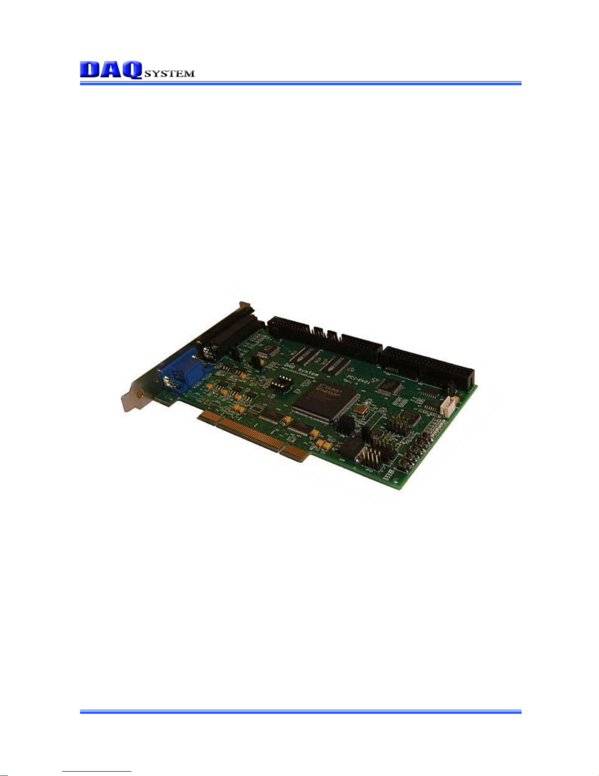
1. PCI-EK01 Introduction
The PCI-EK01 is specially designed for PCI master and target logic development and an analog data
acquisition board. Also it can be used for multi-purpose applications, for example waveform generator,
ADC(Analog to Digital Converter), DAC(Digital to Analog Converter), high current driver and high speed
analog data logger.
[Figure 1-1. PCI-EK01 Functional Blocks]
PRODUCT INFORMATION
Application
PCI development and evaluation
Data acquisition
Laboratory instrumentation
Process control systems
Factory automation
Specification
General
PCI Target 32bit/33Mhz, 5V/3.3V compatible
Full 33Mhz burst read/write operation
Average data rate is 30MB data to, 8MB data from the board without
DMA.
Analog
Input/
Output
Digital
Input/
Output
Counter/
Timer
PCI Core Logic
(FPGA)
High
Speed
SRAM
Page 4

PCI-EK01 Users Manual (Rev 1.0)
-4- http://www.daqsystem.com
Very flexible to upgrade because of FPGA is used as PCI bridge and
overall board
Analog Input
12bit resolution/ 8 Single ended or 4 differential input
0 to +3.3V, ±1.65V input range/ MAX 200Ksps(5uSEC) conversion
time
Can change sampling interval in auto scanning mode by 2.5uSEC
increment
Power on auto-calibration/ ±1 (LSB) INL/DNL
±1uA analog input leakage current/ 20pF analog input capacitance
On-board 1024 x 16 data FIFO/ On-board 256K(type A) x 16 data
SRAM
Analog Output
12bit resolution/ 4 channel output/ 0 to +3.3V output range
MAX 1M (1uSEC) update rate
Can change update interval in waveform generation mode by 1uSEC
increment
Simultaneous update of outputs
±16 (LSB) INL/ ±1 (LSB) DNL/ ±3 (LSB) Offset error/ Slew Rate
0.7V/usec
On-board 1024 x 16 waveform generation dual-port RAM
Digital I/O
On-board 82C55 chip/ 24bit general purpose I/O
Three 8bit group(Port A/B/C)/ 3.3V CMOS logic level
Port B has high current sink capability (max 500mA)
Timer/Counter
32-bit Timer/ 32-bit Counter
Input frequency max 60Mhz/ 25n timer resolution
One-shot or alternate timer output mode/ 3.3V CMOS logic level
Software
Supported OS
Windows 2000/XP/Windows 7
API
Kernel mode WDM Driver/ User mode DLL
Test Application(Waveform Generator, Waveform Display)
Page 5
PCI-EK01 Users Manual (Rev 1.0)
-5- http://www.daqsystem.com
2. Installation
You confirm whether or not the packing contents are in good order before installation.
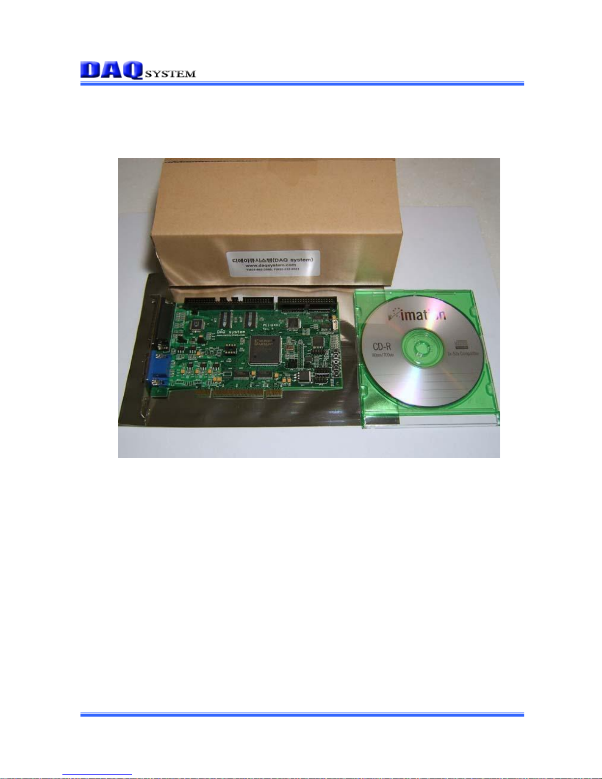
2.1 Confirm Contents
[Figure 2-1. PCI-EK01 Product Contents]
Product Contents
1. PCI-EK01 Board
2. Windows2000/XP Driver (CDROM)
3. Application Sample Source (CDROM)
4. Schematic/Part List etc (CDROM)
2.2 Hardware Installation
For PCI-EK01 board installation to PC is as follows. There isn’t a jumper especially to set up for
board installation in case of PCI boards because it is Plug & Play devices.
(1) First, turn off the power.
(2) Take off the computer case, and PCI-EK01 connects to empty slot. At this time, you like to use
Page 6
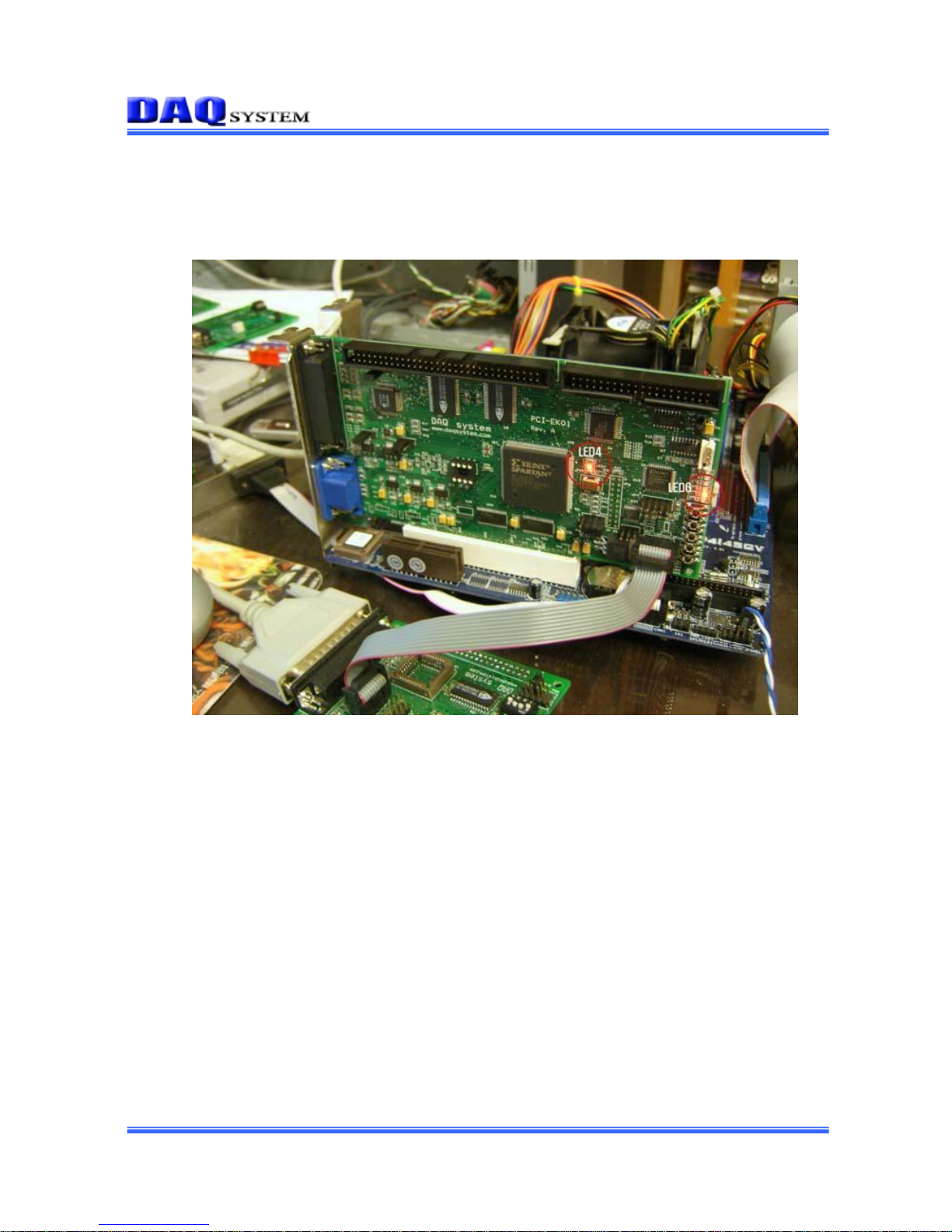
PCI-EK01 Users Manual (Rev 1.0)
-6- http://www.daqsystem.com
the slot that is close to a CPU side with a lot of empty slots.
(3) After bracket of board fix to computer by using a screw, close the case.
(4) Turn on the switch after assembly.
[Figure 2-2. PCI-EK01 connect to PC]
* Above picture shows no PC case for user understanding. Generally it use in case of PC
mother board.
(5) When the power on, two LED is lighting on like Figure 2-2. If the board finishes the configuration
Normally, A LED4 lights on. A LED6 lights on/off per 1 second in order to ideal of clock.
(6) From LED1 to LED5 light on in order to PCI bus operation.
Page 7
PCI-EK01 Users Manual (Rev 1.0)
-7- http://www.daqsystem.com
2.3 Software installation
After hardware installation, you install a Driver and sample application program on CPU board. You
use a CD that provided it to a box for installation.
The installation order is as follows, explain Windows XP with basis if there isn’t special explanation.
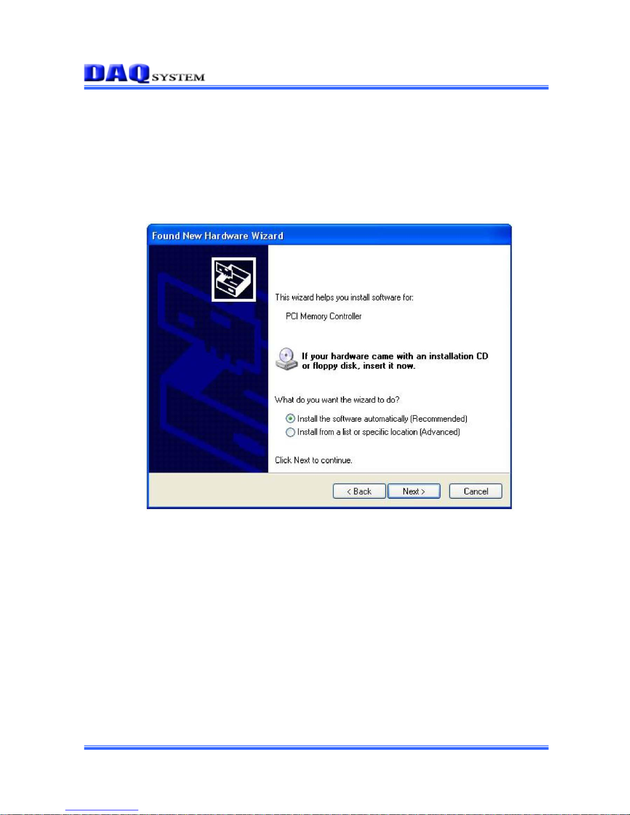
(1) After finished booting that you can show the picture of “Found New Hardware Wizard” window.
Select the item “Install from a list or specific location (Advanced)” and click “Next”.
[Figure 2-3. PCI-EK01 Device Search Window]
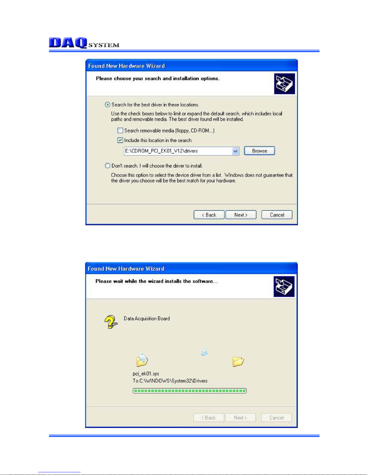
(2) Insert the accompanying CDROM in the CDROM driver and press the “Browse” to point out the
folder which contains the Driver. ex) F:\CDROM_PCI_EK01\drivers
The driver folder includes a file of “pci_ek01.inf” and “pci_ek01.sys” that it is necessary for
driver installation.
Page 8
PCI-EK01 Users Manual (Rev 1.0)
-8- http://www.daqsystem.com
[Figure 2-4. PCI-EK01 Device Driver Search Window]
A warning message appears during installation here, press “Continue Anyway” button.
You can show below message window. Process progress as follows.
Page 9
PCI-EK01 Users Manual (Rev 1.0)
-9- http://www.daqsystem.com
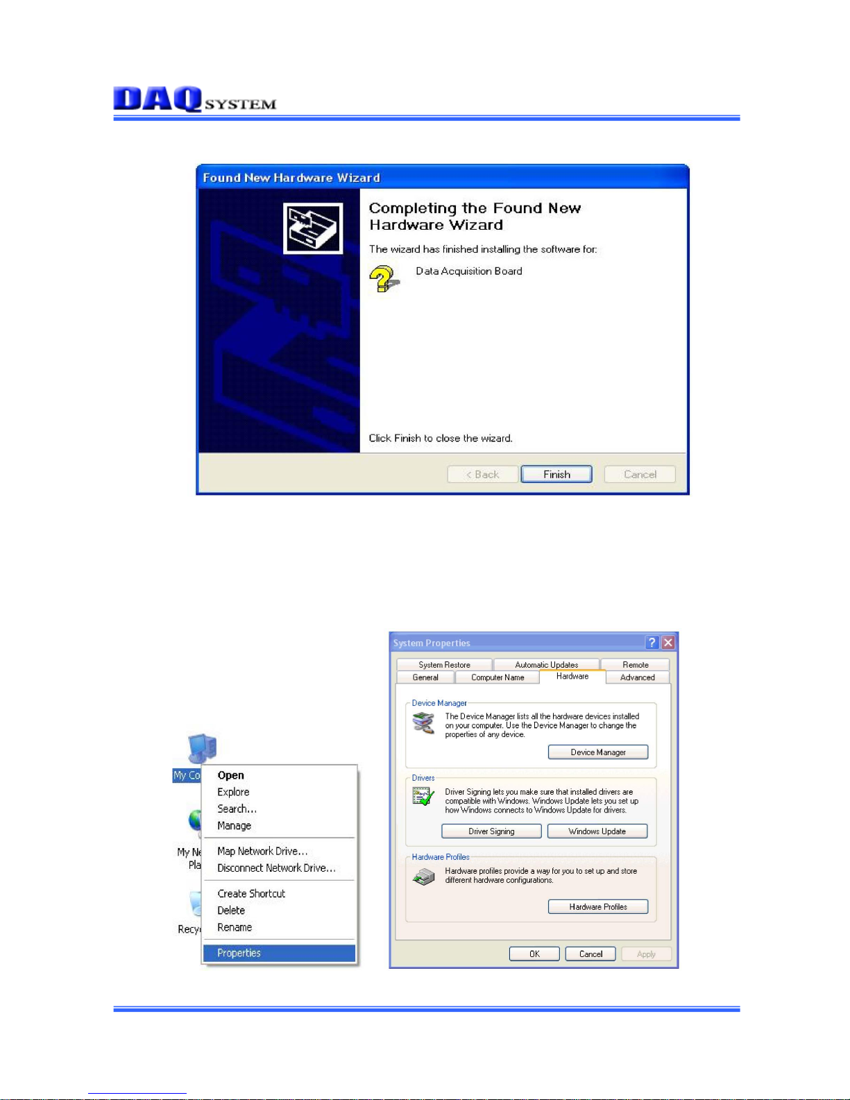
(3) If the installation is completely finished, you can show below message window.
[Figure 2-5. PCI-EK01 Completing Device Driver Window]
(4) If the installation is completely finished, you can use the USB-DIO6400 board.
But, it confirm a driver normally installation in the following ways. Do the following steps to show
up the “Device Manager” window. [My Computer -> Properties -> Hardware -> Device Manager ->
Multifunction Adaptors -> “PCI-EK01”]
[Figure 2-6. “System Properties” window-“Hardware” Tab]
Page 10
PCI-EK01 Users Manual (Rev 1.0)
-10- http://www.daqsystem.com
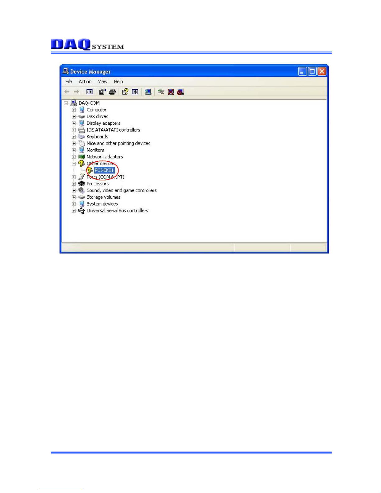
[Figure 2-7. “Device Manager” window]
If you can see the “PCI-EK01” at Multifunction Adaptors, the driver installation is to have been
over. (Check the red circle)
Important Notice : After installation, you should re-boot the system for the proper operation.
Page 11
PCI-EK01 Users Manual (Rev 1.0)
-11- http://www.daqsystem.com
3. PCI-EK01 Board Explanation
It simply explains about board functions. Refer to a “Specification part” regarding a detailed function.
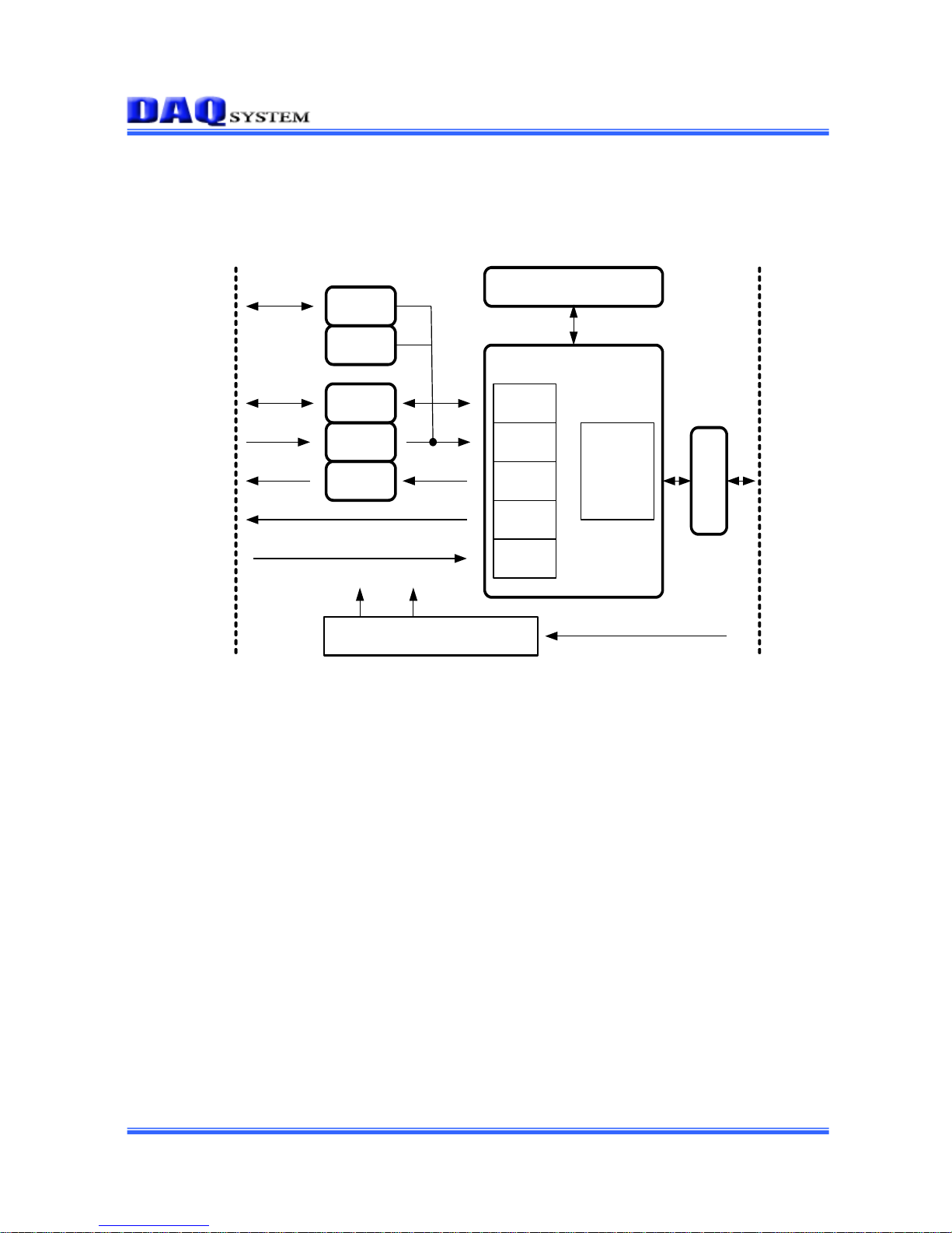
3.1 PCI-EK01 Function
POWER DISTRIBUTION
DPRAM
ADC
Core control
PCI BUS
TIMER
COUNTER
FIFO
UART
TARGET
PCI
INTERFACE
DAC
T/Rx
USER I/O
SRAM
I/O
Switch & LED
LEVEL
SHIFTER
[Figure 3-1. PCI-EK01 Block Diagram]
Figure 3-1 shows that the PCI-EK01 has a lot of functions for various test. Each configuration
function is as follows.
(1) Core Control
The PCI-EK01 composes a PCI Target, external ADC, DAC interface and FIFO/TIMER/Counter
with using a FPGA (Spartan3). It is not used a UART function, it will be upgrade later.
(2) Level Shifter
A Level shifter exchanges a logic level of PCI to a logic level of FPGA. So, it is handily usable
just place to a slot without jumper setup of PCI 3.3V system or PCI 5V bus system.
(3) Power Distribution
It gets from 5V power at PCI bus and it supply as making the necessary 1.2V, 2.5V, 3V, 3.3V
power to use at board.
Page 12

PCI-EK01 Users Manual (Rev 1.0)
-12- http://www.daqsystem.com
(4) Switch & LED
There is the LED which can confirm action state of a board. There are 5 switches 매 that a
user test it to a manual.
(5) I/O
It can interface with the outside by 24bit I/O as it equip 82C55. It is a 3.3V logic level and 8bits
of these 24bits can drive 500mA.
(6) SRAM
It is used to high speed data transfer (Max 33Mhz) and ADC’s data buffer as it equip
maximum 8Mbit(1M Byte) high speed RAM.
(7) T/Rx
It is a RS232C Transceiver. It can use it to connect at PC or device.
(8) ADC
It’s an Analog to Digital Converter. It can use the methods of 8-Ch Single Ended or 4-Ch
Differential, can make sampling 200K(5uSEC) per second.
(9) DAC
It’s 4-Ch Digital to Analog Converter, it can update a DAC’s value with maximum 1M (1uSEC).
Page 13

PCI-EK01 Users Manual (Rev 1.0)
-13- http://www.daqsystem.com
3.2 Address Map
As it uses CPU of the x86 system which we use mainly, it can classify greatly it to memory and I/O
area. In order to support Plug & Play in case of PCI bus that has a special Configuration. It can save
the resource and device state control register etc.
Memory Area
I/O Area
Configuration
Area
4G
64K
64DWORD
[Figure 3-2. Address Map of IBM PC Series]
The PCI-EK01 use a memory and I/O that have been assigned to system for operation, the contents
are as follows that they required.
Memory Max. 64MByte
I/O 256Byte
An area of assigned address in PCI-EK01 is used like Figure 3-3. All peripheral device’s control and
status register located in I/O area, only high speed SRAM located in memory area.
Page 14

PCI-EK01 Users Manual (Rev 1.0)
-14- http://www.daqsystem.com
[Figure 4-3. PCI-EK01 Address map]
(Notice) 1. Currently it is not used a UART function, it will be upgrade later.
2. Currently it is not used a VGA function, it will be upgrade later.
Page 15

PCI-EK01 Users Manual (Rev 1.0)
-15- http://www.daqsystem.com
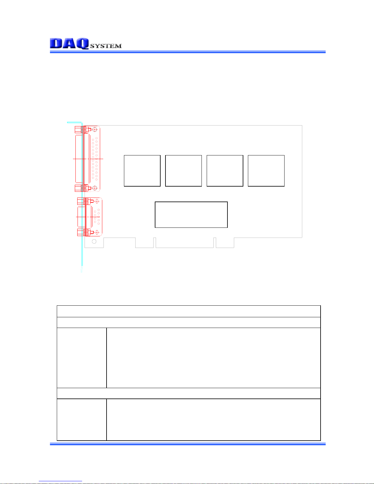
3.3 Jumper Option and Connector Pin-out
The PCI-EK01 is prepared a lot of Jumpers and Connectors. Each Jumper & Connector is used to
select a function and extend a function, basic setting recommands that you use it with state set up in
case of product shipment. But, a user can exchange setting and connection for special test. Yhis
chapter will be explained this situation.
JP4
JP5
JP2
JP12JP11
JH1
JP1
P1
P2
JP3
LED4
JP6
JP8
JP9
JP7
JP13
JP10
SW1
SW2
SW3
SW4
SW5
COM1
LED1
LED2
LED3
LED5
LED6
LED7
Y1
[Figure 3-4. PCI-EK01 External Connection & Jumper]
[Table 1. Connector and Jumper List]
No.
Name
Description
Remark
1
P1
Analog Input/Output, Counter/Timer
2
P2
VGA video signal
Future Upgrade
3
JH1
Local Address & Data Bus
4
JP1
Digital Input/Output
5
JP2
ADC Reference Voltage
Close
6
JP3
Select Digital Power
3.3V or 5V
7
JP4
DAC Power Selection
AVCC or DVCC
Page 16

PCI-EK01 Users Manual (Rev 1.0)
-16- http://www.daqsystem.com
8
JP5
DAC Reference Voltage Selection
ADC reference out or
DAC Power
9
JP6
FPGA Parallel configuration
Not used
10
JP7
EPLD(XC9536XL) JTAG
11
JP8
FPGA configuration Mode Selection
12
JP9
Serial Flash Mode Selection
Future Upgrade
13
JP10
FPGA & Serial Flash Program JTAG
14
JP11
+/- 12V Power
Not used
15
JP12
PCI I/O Power
Not used
16
JP13
User defined Jumper – Connection Tact Switch
17
LED1-3
LED5
For PCI Transition Monitor
18
LED4
FPGA configuration Indicator
19
LED6
Clock Indicator
20
LED7
PCI Target select
21
SW1-3
User Definition
Not used
22
SW4
FPGA Re-configuration
23
SW5
User Definition
Not used
24
COM1
RS232C
Future Upgrade
25
Y1
User Definition Clock
A user gets arbitrary clock at Timer/Counter
function so as usable.
Future Upgrade
The basically explanation is like [Table 1]. Each connector jumper continuous explains in detail.
Page 17

PCI-EK01 Users Manual (Rev 1.0)
-17- http://www.daqsystem.com
[P1 Description]
A DSUB-25PIN PLUG connector is connected to Analog Input/Output, Timer Output, Counter
Input. The Analog Input/Output range of ADC & DAC refers to product specification. The
Input/Output level of Timer and Counter is 3.3V CMOS logic level.
Notice) You should use an Analog Ground in case of external interface of an analog signal.
3
10
9
8
7
6
1
2
5
4
19
18
17
16
15
14
13
12
11
25
24
23
22
21
20
Analog Power(+3.3V)
Analog Input 1
Analog Input 7
Analog Input 5
Analog Input 3
Analog Output 0
Analog Output 2
Timer1 Out
Digital Power(+3.3V)
Analog Ground
Counter0 In
Counter2 In
Analog Input 0
Digital Ground
Analog Input 2
Analog Input 4
Analog Input 6
Analog Ground
Analog Output 0
Analog Output 3
Digital Power(+3.3V)
Timer0 Out
Timer2 Out
Counter1 In
Digital Ground
[Figure 3-5. PCI-EK01 P1 Connector Pin-out]
Page 18

PCI-EK01 Users Manual (Rev 1.0)
-18- http://www.daqsystem.com
[P2 Description]
It is not used currently a VGA Video signal, it will be upgrade.
3
10
9
8
7
6
1
2
5
4
15
14
13
12
11
BLUE
GREEN
RED
VSYNC
HSYNC
VGND
VGND
VGND
VGND
VGND
[Figure 3-6. PCI-EK01 P2 Connector Pin-out]
Page 19

PCI-EK01 Users Manual (Rev 1.0)
-19- http://www.daqsystem.com
[JH1 Description]
We made external interface as it prepared local address and data signal on board to a connector so
as to be easy. A user can easily add the hardware function with this connector.
3
109
87
6
1 2
5
4
19
1817
1615
1413
1211
2423
2221
20
VDD(+3.3V)VDD(+3.3V)
33
3231
3029
2827
2625
3837
3635
34
47
4645
4443
4241
4039
5251
5049
48
62
59 60
57 58
55 56
53 54
63 64
61
DATA 0
DATA 1
DATA 2
DATA 3
DATA 4
DATA 5
DATA 6
DATA 7
DATA 8
DATA 9
DATA 10
DATA 11
DATA 12
DATA 13
DATA 14
DATA 15
BYTE EN1 LOW#
BYTE EN1 HIGH#
OE#
ADDRESS 00
ADDRESS 01
ADDRESS 02
ADDRESS 03
ADDRESS 04
ADDRESS 05
ADDRESS 06
ADDRESS 07
ADDRESS 08
ADDRESS 09
ADDRESS 10
ADDRESS 11
ADDRESS 12
ADDRESS 13
ADDRESS 14
ADDRESS 15
ADDRESS 16
ADDRESS 17
Digital Ground
WE#
CE1#
Digital Ground
DATA 27
DATA 28
DATA 29
DATA 30
DATA 31
BYTE EN2 LOW#
BYTE EN2 HIGH#
CE2#
Digital Ground
DATA 16
DATA 17
DATA 18
DATA 19
DATA 20
DATA 21
DATA 22
DATA 23
DATA 24
DATA 25
DATA 26
Digital Ground
[Figure 3-7. PCI-EK01 JH1 Connector Pin-out]
Page 20

PCI-EK01 Users Manual (Rev 1.0)
-20- http://www.daqsystem.com
[JP1 Description]
It is connected to 82C55 I/O port. It have three 8bits Port (A/B/C), can use input or output
according to program setup. You can see “PORTB DRV 0” ~ “PORTB DRV 7” like under Figure 3-8.
This is connected by driver that applied a lot of current. (Refer to Schematic)
3
109
87
6
1 2
5
4
19
1817
1615
1413
1211
2423
2221
20
PVCC(+3.3V/5V)PVCC(+3.3V/5V)
33
3231
3029
2827
2625
3837
3635
34
4039
PORTB 0
PORTB 1
PORTB 2
PORTB 3
PORTB 4
PORTB 5
PORTB 6
PORTB 7
Digital Ground
PORTC 0
PORTC 1
PORTC 2
PORTC 3
PORTC 4
PORTC 5
PORTC 6
PORTC 7
Digital Ground
PORTA 0
PORTA 1
PORTA 2
PORTA 3
PORTA 4
PORTA 5
PORTA 6
PORTA 7
Digital Ground
PORTB DRV 0
PORTB DRV 1
PORTB DRV 2
PORTB DRV 3
PORTB DRV 4
PORTB DRV 5
PORTB DRV 6
PORTB DRV 7
EXT RESET
Digital Ground
[Figure 3-8. PCI-EK01 JP1 Connector Pin-out]
Page 21

PCI-EK01 Users Manual (Rev 1.0)
-21- http://www.daqsystem.com
[JTAG & Other Connector]
It is prepared an EPLD (Electrically Programmable Logic Device) XC9536XL in case of JP7, for a
program to call Serial Flash and FPGA use it in case of JP10.
It set up a program mode of FPGA in case of JP8. Each program mode setup is as follows.
M2
M1
M0
Configuration Mode
0 0 0
Master Serial
1 1 1
Slave Serial
1 1 0
Master Parallel
0 1 1
Slave Parallel
1 0 1
JTAG
* 1. When connect jumper, it is ‘0’.
* 2. A signal HSWAP_EN has an internal pull-up resistor. When connect jumper, it is ‘0.
If it is “0’, an I/O pin is pull up during configuration period.
A JP13 is connected to switch which it connects in parallel with EPLD. A user uses it when it test
a special function to a manual. (Refer to Schematic)
3
109
87
6
1 2
5
4
GNDVCC(+3.3V)
TDO
TMS
N.C.
N.C.
TCK
TDI
N.C.
N.C.
3
87
6
1 2
5
4
GNDSWITCH 2
GND
GND
GND
SWITCH 3
SWITCH 1
SWITCH 5
3
87
6
1 2
5
4
GNDHSWAP_EN
GND
GND
GND
MODE 0
MODE 1
MODE 2
JP8
JP13
JP7/JP10
Page 22

PCI-EK01 Users Manual (Rev 1.0)
-22- http://www.daqsystem.com
[Default Jumper Setup]
A JP3 select a I/O connector (JP1) power. It is +3.3V in case of connection 1-2. It is +5V in case of
connection 2-3.
A JP4 can select DVCC or AVCC to the power of DAC chip. The last jumper (JP5, JP6) likes to
use it with default setting as it refers to a schematic.
3 12
31 2
3 12
JP4 JP5JP3
31 2
JP9
[RS232C]
It prepared by preparation so as to be able to equip an UART function. The PCI-EK01 has a
RS232C Transceiver that it connected COM1 and FPGA.
3
1
2
Receive
Transmit
Signal Ground
COM1
Page 23

PCI-EK01 Users Manual (Rev 1.0)
-23- http://www.daqsystem.com
3.4 CDROM Folder Explanation
The board which accompanying CDROM includes a sample source that user can install and test
and program at PC.
First, the “drivers” folder has Driver and Install File, the “manual” folder has User
Manual/Schematic/Application Note etc.
The “Sample” folder has some Source and execution file of the “PCITest”.
The “readme” folder has the newest files and files which user shall read it before installation.
Page 24

PCI-EK01 Users Manual (Rev 1.0)
-24- http://www.daqsystem.com
4. Sample Program & Test
This chapter explains that a functional test to learn usage and check products for defects. The test
performs a “PCITest.exe” program in a SAMPLE folder in CDROM at the PC that PCI-EK01 was
installed.
The SAMPLE folder of CDROM includes a execution file and source file of “PCITest.exe”. The sample
source files can use that a user modifies in order to implement a necessary function.
1 2 3 4 5 6
7
8
9
10
11
12
13
14
15
16
17
18
19
20
21
22
[Figure 4-1. “PCITest.exe” Execution Screen]
Above picture is an execution screen of “PCITest.exe” program. First, the method of using program
will be explained. Each control will be written the number at screen. Meaning and using method to see in
Page 25

PCI-EK01 Users Manual (Rev 1.0)
-25- http://www.daqsystem.com
each numbers are as follows.
No.
Name
Description
Remark
1
Memory
read
When press button, it read from 0 to 100000h (total
1MByte) at memory and mark a number (8) area.
2
Memory
Write
When press button, it progressively write from 0 to
100000h at memory. So, first after execution “Memory
Write” and then execute “Memory Read”, it confirms a
correct data.
(Notice)When memory read/write, an Auto bit of ADC
becomes certainly ‘0’.
3
Access
Bits
It set up how does unit of the byte deal in case of
reading and writing at memory.
Not apply Currently
Always deal with
32bits
4
Write At
It record designated data to a specific address area by
32 bits word.
5
Memory
Offset
When data value record to a specific address of memory,
it is a value of offset
16bit
Hexa-Decimal
6
Memory
Write Data
The data that will be written to a specific address of
memory.
When the data record to a specific address of memory, it
set up a value of Offset and Data that wanted value,
after that press “Write At” button. You want check
whether exactly writing or not, you can confirm to press
“Memory read” button.
16bit
Hexa-Decimal
7
Progress
Bar
It marks a progress situation, when the memory reading.
8
Memory
Data
It marks a data which read it to memory.
9
I/O Write
When press button, it is writing specific I/O address.
10
I/O Read
When press button, it mark to a screen as reading
specific I/O address.
11
I/O Offset
It set up Offset of the address that it want to read or write
in I/O area.
16bit
Hexa-Decimal
12
I/O Read
Count
It set up I/O data amount to read.
* The reading or writing if I/O is always 32bit DWORD.
Not apply Currently
Page 26

PCI-EK01 Users Manual (Rev 1.0)
-26- http://www.daqsystem.com
13
I/O Write
Data
It set up writing data in I/O.
16bit
Hexa-Decimal
14
I/O Auto
Increment
It set up automatically increase I/O address in case of
reading or writing several I/O data.
Not apply Currently
15
DAC FIFO
Write
Points
It set up how many point unit write to DAC FIFO for
Waveform Generation.
It is the point from 1 to maximum 1000.
16
DAC FIFO
Write
It is writing the data above points at FIFO.
* Writing data is a Sine wave.
17
I/O Read
Data
It marks a data which read it to specific address in I/O.
18
ADC
Run/Stop
When press button, it reads value of ADC at buffer
periodically (0.5 sec) and will run or stop at screen.
19
ADC
Channel
Enable
The ADC value can mark a lot of channels at screen, it
set up the channel which it wants to display.
It marks 4 channels at program.
20
Time Knob
It set up an axis of time if it marks ADC value to a
screen.
Not apply Currently
21
Voltage
Knob
It set up an axis of voltage if it marks ADC value to a
screen.
Not apply Currently
22
ADC
Graph
It marks ADC data on the screen.
(Remark)
1. The PCITest program uses an ActiveX for making ADC Graph so that you shall install specific OCX in
order to perform it. (Refer to CDROM for registration way)
2. If it performs a program at Windows 2000, you shall a copy “GDIPlus.dll” to execution folder or
Windows system folder. It is not necessary to copy a file “GDIPlus.dll” at Windows XP because XP
have one.
3. If you want to compile of PCITest sample source, you shall install the OCX and Windows platform
SDK. You can download a SDK at Micro Soft web site.
4. This program test and compile with Visual C++ 6.0/Service Pack 5.
5. System Recommend
Pentium 3 over or compatible PC (Pentium 2 is possible)
RAM 256M over (RAM 64M is possible)
Monitor 1024 x 768 over
Hard Disk 10G over
Page 27

PCI-EK01 Users Manual (Rev 1.0)
-27- http://www.daqsystem.com
Windows XP Professional or Windows 2000
6. Refer to AN203(PCI-EK01-Register Level Application Guide)
4.1 Analog Output
(1) DAC FIFO Write Points input “1000” and press DAC test(DAC FIFO Write) button. It will record a
sine wave data of 1000 points for making waveform at DAC FIFO.
The 1000 points is a data from DAC channel 0 ~ 3.
(2) After I/O address offset input “94 and Data input “1”, press I/O Write button.
(3) User confirm whether or not sine wave is displayed on P1(D-sub 25pin plug) connector as it use
Oscilloscope like Figure 4-2.
[Figure 4-2. Connection for Test]
Page 28

PCI-EK01 Users Manual (Rev 1.0)
-28- http://www.daqsystem.com
[Figure 4-3. Confirm an Analog Output]
(4) The output is displayed all 4 Analog out. It confirms all 4 channels as it use Oscilloscope.
(5) You can use Wave form generator like Figure 4-4 for Wave form generation.
[Figure 4-4. Wave Form Generator]
Page 29

PCI-EK01 Users Manual (Rev 1.0)
-29- http://www.daqsystem.com
4.2 Analog Input
(1) It connect number 6 (Analog out 0) and number 14 (Analog In 0) of P1(D-sub 25pin plug)
connector with jumper line.
(2) After I/O address offset input “84” and Data input “0”, press I/O Write button.
It stops automatic action of ADC. This is a test for high speed SRAM that used0 ADC buffer.
(3) Press Memory Write button and again press Memory Read button. As a result, it display memory
data. User confirms that “0” to 0 address, “3FFFF” to a FFFFCh address whether or not a record is
made to double word.
(4) I/O address offset input “84” and Data input “44” after that press I/O Write button.
[Figure 4-5. DaqScope Program]
(5) You execute a DaqScope program like Figure 4-5. When press RUN/STOP button, it will mark a
ADC value of Analog out channel to a screen.
(6) Press ADC Channel Enable button, it display your wanted channel.
(7) Again start RUN/STOP button, it will stop the display of ADC value.
4.3 Digital Input/Output
(1) I/O address offset input “84” and Data input “0”, press I/O Write button. It stops automatic action
of ADC, it use to control and local address and data bus by 82C55.
Page 30

PCI-EK01 Users Manual (Rev 1.0)
-30- http://www.daqsystem.com
(2) I/O address offset input “A0” and Data input “80”, press I/O Write button.
=>All port (A/B/C) output of 82C55 will make Mode 0.
(3) I/O address offset input “A4” and Data input “FF”, press I/O Write button.
=>”A” port of 82C55 record a “FF”.
(4) It confirms whether or not output exactly come out as refer to specification Oscilloscope and JP1
connector.
(5) I/O address offset input “A4” Data input “0”. After press I/O Write button, check the output od
Oscilloscope. It record “FF” of 82C55 A port.
(6) In the above test (3) ~ (4), you perform it to a port B/C.
4.4 Counter
(1) I/O address offset input “8” and Data input “1”, press I/O Write button.
=> It is enable Counter 0 action.
(2) I/O address offset input “4” and Data input “3”, press I/O Write button.
=> Target setup counter records “3”.
(3) The counter 0 input (Pin #11) of connector P1 apply High Active pulse at once. After that, I/O
address offset input “0” and press I/O Read button. It confirms that current count make “1”.
(4) It apply count pulse two times more. It confirm count over occurrence as reading a STATUS
register counter 0 and current counter value is “3”.
(5) There is 3 Counter at PCI-EK01, remaining two counters shall test as above.
4.5 Timer
(1) I/O address offset input “34” and Data input “4”, press I/O Write button.
=> It loads a Timer 0 setup value to a register.
(2) I/O address offset input “38” and Data input “5”, press I/O Write button.
=> It turns over output in case of time-out at Auto-reload mode to frequency 0. At this time 5MHz
works if it try to confirm frequency. If it shows to formula
Frequency = 25M / (TMR_SET + 1)
A TMR_SET value shall over minimum 1.
(3) As result timer, it confirms that #22 (Timer 0) of P1 connector connect to Oscilloscope because
output works at pin #22.
(4) I/O address offset input “38” and Data input “d”, press I/O Write button.
=> It prints out 20nSEC pulse in case of time-out at Auto-reload mode to frequency 0. At this time
10MHz works if it try to confirm frequency. If it shows to formula
Frequency = 50M / (TMR_SET + 1)
A TMR_SET value shall over minimum 1.
(5) There is 3 Timer at PCI-EK01, remaining two timers shall test as above.
Page 31

PCI-EK01 Users Manual (Rev 1.0)
-31- http://www.daqsystem.com
5. Specification
Various functions are included to the PCI-EK01 in order to test.
5.1 General Information
General specification of board is as follows. Basically most function made by FPGA, a main purpose
is that ADC (Analog to Digital Converter) or DAC (Digital to Analog Converter).
▣ Flexible Board
▪ PCI Target 32bit/33Mhz
▪ PCI 5V/3.3V compatible
▪ Full 33Mhz burst read/write operation
▪ Average data rate is 30MB data to, 8MB data from the board without DMA.
▪ Very flexible to upgrade because of FPGA is used as PCI bridge and overall board control.
▪ Spartan 3 (XC3S500-type A)
▪ Spartan 3 (XC3S200-type B)
▪ 4Mbit(256K x 16) fast SRAM
▪ 5 user input tact switch
▪ 6 user definable output LED indication
▪ User expandable local memory through 64pin header connector.(3.3V operation)
▪ user selectable oscillator
▪ Video interface (type B only)
▪ UART interface (type B only)
5.2 Hardware
▣ Analog input
▪ 12bit resolution
▪ 8 Single ended or 4 differential input
▪ 0 to +2.5V, ±1.25V input range(0 to+3.3V, ±1.65V input range changeable)
▪ MAX 200Ksps(5uSEC) conversion time
▪ Can change sampling interval in auto scanning mode by 2.5uSEC increment
▪ Power on auto-calibration
▪ ±1 (LSB) INL/DNL
▪ ±1uA analog input leakage current
▪ 20pF analog input capacitance
▪ On-board 1024 x 16 data FIFO
▪ On-board 512K(type B) x 16 data SRAM
▪ User can select ADC data storage, FIFO or SRAM
▪ In auto scanning mode, user can select any channel order.
▪ For more information, please refer to ADC(AD7859AS) specification on analog
Web-site(http://www.analog.com)
▣ Analog output
▪ 12bit resolution
▪ 4 channel output
▪ 0 to +3.3V output range
▪ MAX 1M (1uSEC) update rate
▪ Can change update interval in waveform generation mode by 1uSEC increment
▪ Simultaneous update of outputs
Page 32

PCI-EK01 Users Manual (Rev 1.0)
-32- http://www.daqsystem.com
▪ ±16 (LSB) INL
▪ ±1 (LSB) DNL
▪ ±3 (LSB) Offset error
▪ ±1 (LSB) Gain error
▪ Slew Rate 0.7V/usec
▪ On-board 1024 x 16 waveform generation dual-port RAM
▪ In waveform generation mode, user can select any channel order.
▪ For more information, please refer to DAC(AD5324A) specification on analog
Web-site(http://www.analog.com)
▣ Digital I/O
▪ On-board 82C55 chip
▪ 24bit general purpose I/O
▪ Three 8bit group(Port A/B/C)
▪ Port B has high current sink capability (max 500mA)
▪ 3.3V CMOS logic level
▪ Power on floating or logic low
▣ Timer/Counter
▪ Three 32-bit Timer
▪ Three 32-bit Counter
▪ Input frequency max 60Mhz
▪ 25n timer resolution
▪ One-shot or alternate timer output mode
▪ 3.3V CMOS logic level I/O interface
▣ External connection
▪ 25pin D-sub(Analog in-out, timer/counter)
▪ 64pin Box-header(Local memory bus)
▪ 40pin Box-header(Digital I/O)
5.3 Software
▣ Operating system
▪ Windows 2000/XP and Windows 7
▣ Application Programming Interface
▪ Direct control through WDM driver
▪ Windows DLL API
▣ Software Development Kits
▪ User who have strong interest in developing PCI DAQ board can buy SDK.
▪ SDK contents
- Basic VHDL source
- WDM Driver source
- DLL source
- Test Application(Waveform generator/Waveform Display)
▪ For more information including price, Please contact us
Page 33

PCI-EK01 Users Manual (Rev 1.0)
-33- http://www.daqsystem.com
5.4 Physical/Environment
▣ Dimensions
▪ Standard Universal(5V/3.3V) PCI 32bit form-factor(175mm x 95mm)
P1
P2
175
95
▣ Temperature
▪ 0 to 70℃, operating
▪ -20 to + 80℃ storage
▣ Relative Humidity
▪ 20 to 80 percent, non-condensing
▣ Power Requirement
▪ +5VDC(±5%) at max 1A
Page 34

PCI-EK01 Users Manual (Rev 1.0)
-34- http://www.daqsystem.com
References
1. PCI System Architecture
-- MindShare Inc.
2. PCI Local Bus Specification
-- PCI-SIG
3. PCI-EK01 Register Level Application Guide
-- DAQ system
4. PCI-EK01 Driver Level Programming Guide
-- DAQ system
5. General information on PCI board API
-- DAQ system
6. 82C55 chip manual
-- Intel corp.
 Loading...