

Page 1
PCIe-DIO05 Users Manual (Rev 1.1)
-1- http://www.daqsystem.com
PCIe-DIO05
User’s Manual
Windows, Windows2000, Windows NT and Windows XP are trademarks of Microsoft. We acknowledge that the
trademarks or service names of all other organizations mentioned in this document as their own property.
Information furnished by DAQ system is believed to be accurate and reliable. However, no responsibility is assumed by DAQ
system for its use, nor for any infringements of patents or other rights of third parties which may result from its use. No license is
granted by implication or otherwise under any patent or copyrights of DAQ system.
The information in this document is subject to change without notice and no part of this document may be copied or
reproduced without the prior written consent.
Copyrights 2007 DAQ system, All rights reserved.
Page 2

PCIe-DIO05 Users Manual (Rev 1.1)
-2- http://www.daqsystem.com
Contents
1. PCIe-DIO05 Block Diagram
2. Connecter Pin Map
2.1 External DSUB-37PIN
2.2 Internal BOX-40PIN
3. Installation
3.1 Confirm Contents
3.2 Installation Sequence
4. Board Function
4.1 Layout
4.2 Function Description
5. Sample Program
References
Page 3
PCIe-DIO05 Users Manual (Rev 1.1)
-3- http://www.daqsystem.com
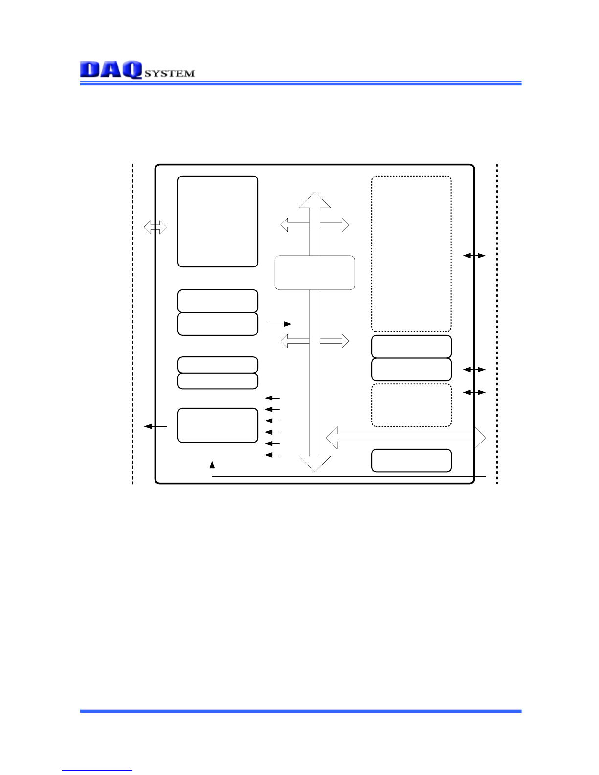
1. PCIe-DIO05 Block Diagram
PCI BUS
PCIe-DIO05 INTERNAL BLOCK
PCI Target
/ Master
Local Bus
Address
Data(Mem,I/O)
Reserved
(0x00 – 0x5F)
DIO 32bit Input
(0xC0)
Interrupt controller
Ext. Address, Data, Control
Local BUS
Interrupt
Controller
(0xb0)
INT sources in Chip
IO Decoder
MEM Decoder
To each IO
Module
DPRAM
From Ext.
CLOCK syn.
MEM Decoder
BUS Mux
Reserved
(0xD0 – 0xFF)
[Figure 1-1. PCIE-DIO05 Internal Block Diagram]
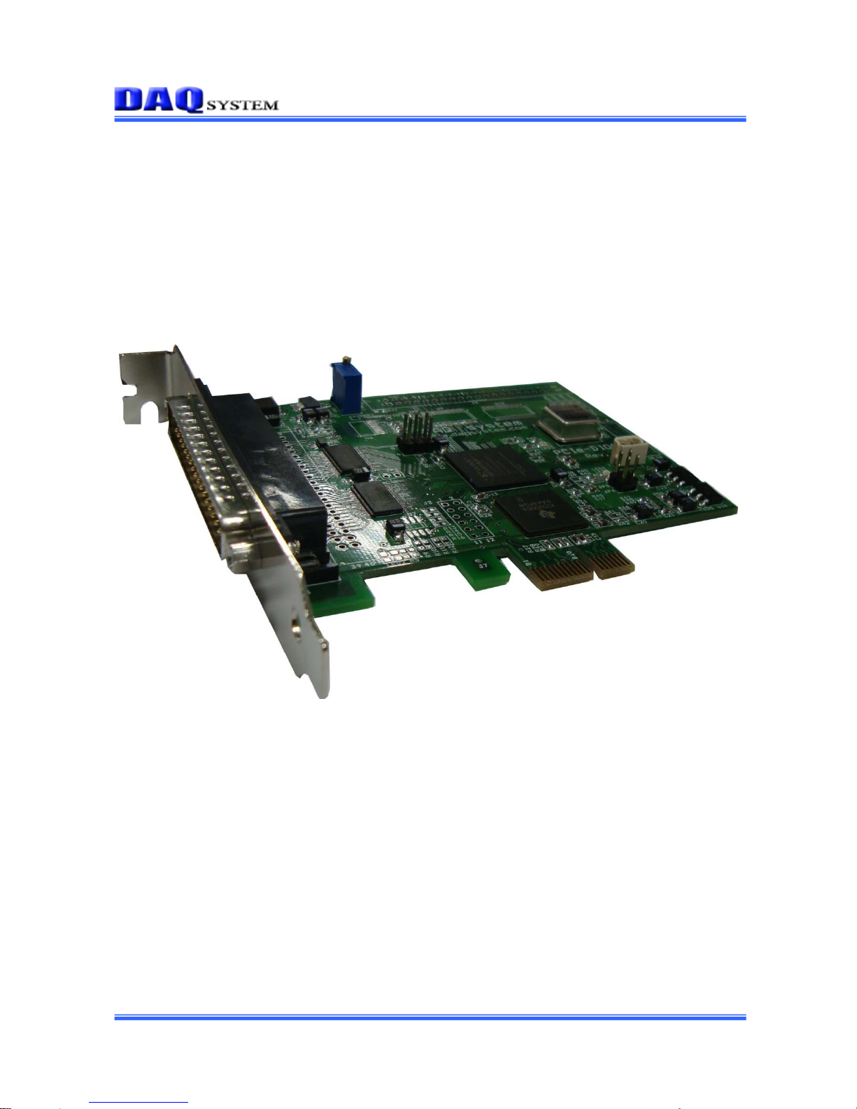
The PCIe-DIO05 is a board having the function of external with the 32 TTL level input port. This
product is designed for High speed digital data logger with PCI Express Interface.
Page 4

PCIe-DIO05 Users Manual (Rev 1.1)
-4- http://www.daqsystem.com
2. Connecter Pin map
2.1 External DSUB-37PIN
1
20
19
37
3
10
9
8
7
6
1
2
5
4
19
18
17
16
15
14
13
12
11
25
24
23
22
21
20
DIN18
DIN16
DIN10
DIN12
DIN14
DIN8
DIN6
DIN0
DIN2
DIN4
READY
POWER
DIN19
DIN17
DIN15
DIN13
DIN11
DIN9
DIN7
DIN5
DIN3
DIN1
CLOCK
REQUEST
33
32
31
30
29
28
27
26
37
36
35
34
DIN22
DIN24
DIN26
DIN20
DIN28
DIN30
GROUND
DIN31
DIN29
DIN27
DIN25
DIN23
DIN21
[Figure 2-1. PCIe-DIO05 DSUB 37 Connecter]
Page 5
PCIe-DIO05 Users Manual (Rev 1.1)
-5- http://www.daqsystem.com
2.2 Internal BOX-40PIN
3
10 9
8 7
6125
4
19
18 17
16 15
14 13
12 11
25
24 23
22 21
20
33
32 31
30 29
28 27
26
37
36 35
34
38
3940
DIN18
DIN16
DIN10
DIN12
DIN14
DIN8
DIN6
DIN0
DIN2
DIN4
READY
POWER
DIN22
DIN24
DIN26
DIN20
DIN28
DIN30
GROUND
DIN19
DIN17
DIN15
DIN13
DIN11
DIN9
DIN7
DIN5
DIN3
DIN1
CLOCK
REQUEST
DIN31
DIN29
DIN27
DIN25
DIN23
DIN21
N.C
N.C N.C
[Figure 2-2. Internal BOX 40 Connecter]
[Table 1. PCIe-DIO05 Connecter Pin Description]
Pin No.
(DSUB37)
Pin No.
(BOX40)
Pin Name
Description
Remark
1 1 POWER
Board Power Output
2 3 READY
READY 3 5 DIN0
Digital Input 0
4
7
DIN2
Digital Input 2
5 9 DIN4
Digital Input 4
Page 6

PCIe-DIO05 Users Manual (Rev 1.1)
-6- http://www.daqsystem.com
6
11
DIN6
Digital Input 6
7
13
DIN8
Digital Input 8
8
15
DIN10
Digital Input 10
9
17
DIN12
Digital Input 12
10
19
DIN14
Digital Input 14
11
21
DIN16
Digital Input 16
12
23
DIN18
Digital Input 18
13
25
DIN20
Digital Input 20
14
27
DIN22
Digital Input 22
15
29
DIN24
Digital Input 24
16
31
DIN26
Digital Input 26
17
33
DIN28
Digital Input 28
18
35
DIN30
Digital Input 30
19
37
GROUND
Ground 20
2
REQUEST
External TRIGGER Input Signal
21 4 CLOCK
CLOCK Output Signal
22 6 DIN1
Digital Input 1
23 8 DIN3
Digital Input 3
24
10
DIN5
Digital Input 5
25
12
DIN7
Digital Input 7
26
14
DIN9
Digital Input 9
27
16
DIN11
Digital Input 11
28
18
DIN13
Digital Input 13
29
20
DIN15
Digital Input 15
30
22
DIN17
Digital Input 17
31
24
DIN19
Digital Input 19
32
26
DIN21
Digital Input 21
33
28
DIN23
Digital Input 23
34
30
DIN25
Digital Input 25
35
32
DIN27
Digital Input 27
36
34
DIN29
Digital Input 29
37
36
DIN31
Digital Input 31
38
N.C
No Connection
39
N.C
No Connection
40
N.C
No Connection
Page 7

PCIe-DIO05 Users Manual (Rev 1.1)
-7- http://www.daqsystem.com
3. Installation
After unpacking, inspect the board carton to make sure there are no damages on the board.
3.1 Package Content
Product Contents
1. PCIe-DIO05 Board
2. CD (Driver/Manual/API/Sample Source etc.)
3.2 Installation Sequence
To install your PCIe-DIO05 board in your PC, follow the steps described in the document “How
to install PCI DAQ Board” provided by DAQ System. If the document is missing, you can get it from
www.daqsystem.com. The PCIe-DIO05 board is completely Plug & Play. There are no switches or
jumpers to set. Therefore you can install it easily.
- Your OS requirement : Windows 2000 SP4 or Windows XP SP1 above
The PCIe-DIO05 connects to PCI Card Port. After that you can show the below picture of “Found
New Hardware Wizard” window.
If new hardware is found, Wizard will ask you to install the corresponding driver. For installation
of the driver, select the item “Install from a list or specific location (Advanced)” and click “Next”
as in the figure.
Page 8

PCIe-DIO05 Users Manual (Rev 1.1)
-8- http://www.daqsystem.com
The driver folder includes a file of “pci_aio05.inf” and “pci_aio05.sys” that it is necessary for
driver installation. A warning message appears during installation here, press “Continue Anyway”
button. You can show below message window. The process progress as follows.
Page 9

PCIe-DIO05 Users Manual (Rev 1.1)
-9- http://www.daqsystem.com
If the installation is completely finished, you can show below message window.
If the installation is completely finished, you confirm it in the following ways. Do the following
steps to show up the “Device Manager” window. [My Computer -> properties -> Hardware ->
Device Manager -> Multifunction Adaptors -> PCIe-DIO05]
Page 10

PCIe-DIO05 Users Manual (Rev 1.1)
-10- http://www.daqsystem.com
If you can see the “PCIe-DIO05” at Multifunction Adaptors, the driver installation is to have
been over. (Check the red circle)
Notice : After installation, you should re-boot the system for the proper operation.
Page 11

PCIe-DIO05 Users Manual (Rev 1.1)
-11- http://www.daqsystem.com
4. Board Function
In this chapter, the primary functions of the board are described briefly. For more information, refer to
the device specification.
4.1 Layout
[Figure 4-1. PCIe-DIO05 Front side]
The board has three LEDs to indicate the operation status.
LED3 turns on when the board is ready to operate after finished operation.
LED4 turns on when the board transmits the data.
LED5 turns on when power is applied to the board and the initialization ends up.
Page 12

PCIe-DIO05 Users Manual (Rev 1.1)
-12- http://www.daqsystem.com
4.2 Function Description
(1) FPGA
All of the board functions are controlled the FPGA Logic.
(2) Buffer
It receives external digital input.
(3) Regulator
A power supplies to the board.
(4) PCI Express Chipset
It’s a PCI Express Bridge.
(5) EXT VIO
You shall fit it with an external power level as you adjust an equipped volume resistance. A
base setting is 3.3V.
Page 13

PCIe-DIO05 Users Manual (Rev 1.1)
-13- http://www.daqsystem.com
5. Sample Program
DAQ system provides a sample program to make the user be familiar with the board operation and
to make the program development easier. You can find the sample program in the CDROM
accompanying with the board. One of the execution file is “PCIe_DIO05.exe”.
Sample program is provided in source form in order to show the usage of API (Application
Programming Interface) of the board and may be modified for customer’s own usage.
To run the sample application program, you need to use API, it is a form of client DLL. To compile
the sample source to make its executable file, you have to use Import Library files and header files.
You can find them in the CDROM. To run the .exe file, the API DLL file (PCIe_DIO05.DLL) must be in
the same directory with the .exe file or Windows system folder. Another method is to add the directory
of API DLL file to PATH environmental variable.
[Figure 5-1. When Sample program execute]
Page 14

PCIe-DIO05 Users Manual (Rev 1.1)
-14- http://www.daqsystem.com
(1) Select Data Size
It set up data size of input. The data can be input in 32 bits unit. It is transmitting to PC from
PCIe-DIO05 with fixed size.
(2) Stop/Run
Stat/Stop Data collection
(3) Get Data
Get the data on the board. If it is not made of saving to a board like setting number, you shall
wait until storage is finished.
(4) Save to
Save the image frame data of PC to a file.
Page 15

PCIe-DIO05 Users Manual (Rev 1.1)
-15- http://www.daqsystem.com
References
1. PCI System Architecture
-- MindShare Inc.
2. PCI Local Bus Specification
-- PCI-SIG
3. General information on PCI board API
-- DAQ system
4. AN201 How to build application using APIs
-- DAQ system
5. AN312 PCIe-DIO05 API Programming
-- DAQ system
 Loading...