

PUBLICATION NO. 980479
DIGITAL
r
'"
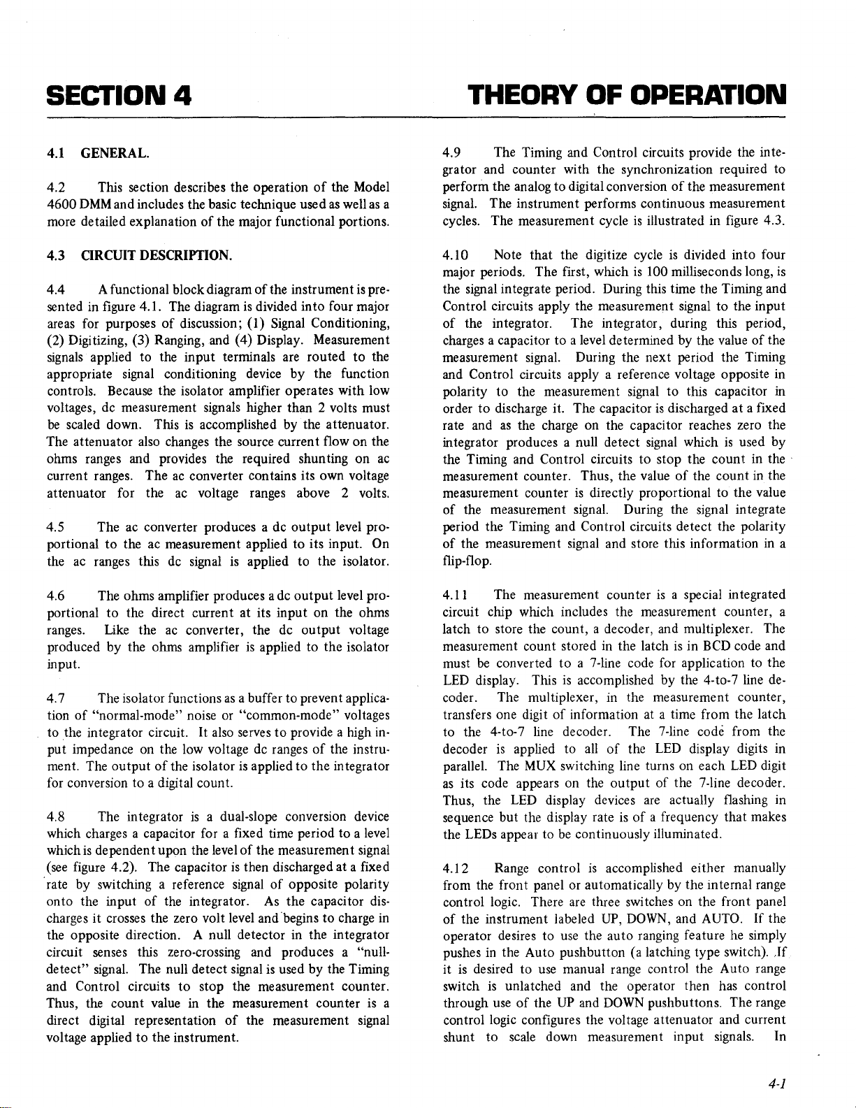
r
00
'-
MULTIMETER
.J '-___
EPT.
""""
-~-
1
u
"
DANA
LABORATORIES,
2401
CAMPUS
IRVINE,
Copyright @ 1977 by
This book or parts thereof may
CALIFORNIA
Dana
laboratories. Inc. Printed in the United States
INC.
DRIVE
92715
PUBLICATION DATE:
not
be reproduced
in
any
form
MAY
without
TELEPHONE
TELETYPE
TELEX
1977
of
written
(714)
910-595-1136
678-341
America.
permission
833-1234
All
rights
of
the publishers.
reserved.

DIGITALY REMASTERED
OUT OF PRINT- MANUAL SCAN
S
By
ArtekMedia
P.O. BOX 175
Welch, MN 55089-0175
Phone: 651-269-4265
www.artekmedia.com
“High resolution scans of obsolete technical manuals”
If you are looking for a quality scanned technical manual in PDF format please visit our WEB
site at www.artekmedia.com or drop us an email at manuals@artekmedia.com
If you don’t see the manual you need on the list drop us a line anyway we may still be able to
obtain the manual you need or direct you to other sources. If you have an existing manual you
would like scanned please write for details. This can often be done very reasonably in
consideration for adding your manual to our library.
Typically the scans in our manuals are done as follows;
1) Typed text pages are typically scanned in black and white at 300 dpi.
2) Photo pages are typically scanned in gray scale mode at 600 dpi
3) Schematic diagram pages are typically scanned in black and white at 600
dpi unless the original manual had colored high lighting (as is the case for
some 70’s vintage Tektronix manuals).
4) Most manuals are text searchable
5) All manuals are fully bookmarked
All data is guaranteed for life (yours or mine … whichever is shorter). If for ANY REASON your
file becomes corrupted, deleted or lost, ArtekMedia will replace the file for the price of shipping,
or free via FTP download.
Thanks
Dave & Lynn Henderson
ArtekMedia
WARRANTY
ARTEKMEDIA => 2012
...
Within one year
your instrument,
or
workmanship. All parts and labor charges will be paid by Dana
Laboratories. Just call Dana
in California, for assistance.
for your prepaid shipment. Your instrument will be returned
freight prepaid.
of
purchase, Dana Laboratories will repair
at
our option,
if
in any way
Product Service
We
will advise the proper shipping address
it
is
defective
at
(714)833·1234 collect
or
in
material
replace
to
you
OPRIETARY NOTICE
This document and the technical data herein disclosed, are proprietary
to
Dana Laboratories, Inc., and shall
of
permission
solicit quotations from a competitive source or used for manufacture
by anyone other than Dana Laboratories, Inc. The information herein
has been developed at private expense, and may only be used for
operation and maintenance reference purposes or for purposes
engineering evaluation and incorporation into technical specifications
and other documents which specify procurement
Dana Laboratories, Inc.
Dana Laboratories, Inc., be used,
not,
without express written
in
whole or in part to
of
products from
of
FOR
ARTEKMEDIA => 2012
Before undertaking any maintenance procedure, whether it
be
described herein or an exploratory procedure aimed at
determining whether there has been a malfunction, read the
applicable section
WARNING and
The equipment described in this manual contains voltages
hazardous
inflicting personal injury. The cautionary and warning
notes are included in this manual to alert operator and
maintenance personnel to the electrical hazards and thus
prevent personal injury and damage to equipment.
If this instrument
through
ensure that the instrument common connector
nected to the ground (earth) connection
mains.
YOUR
a specific troubleshooting or maintenance procedure
of
this manual and note carefully the
CAUTION notices contained therein.
to
human life a,.u safety and which
is
to be powered from the
an
autotransformer (such
as
a Variac
SAFETY
is
capable
AC
or
equivalent)
of
the power
Mains
is
of
con-
Before operating the unit ensure that the protective con-
is
ductor (green wire)
protective conductor
the protective feature
the power cord by using a two conductor extension cord
a three-prong/two-prong adapter.
Maintenance and calibration procedures contained in this
manual sometimes call for operation
applied and protective covers removed. Read the procedures
carefully and heed Warnings
to ensure your personal safety.
Before operating this instrument.
1.
Ensure that the instrument
operate on the voltage available
source.
2.
Ensure that the proper fuse
instrument for the power source
instrument
3. Ensure that
proximity to this instrument are properly grounded
or connected to the protective third-wire earth
ground.
See Installation section.
connected to the ground (earth)
of
the power outlet.
of
the third protective conductor in
of
to
avoid "live" circuit points
is
to be operated.
all
other devices connected to or in
Do
the unit with power
is
configured to
at
the power
is
in
place in the
on
not
defeat
or
which the
TABLE OF CONTENTS
ARTEKMEDIA => 2012
Section Title
1 GENERAL DESCRIPTION
1.1
1.2
1.3 Electrical Description
1.4 Specifications .
2 INSTALLATION & OPERATION
2.1
2.2 Unpacking and Inspection .
2.3 Bench Operation .
2.4
2.5 Power Requirements
2.6 Storage Requirements 2-2
2.7 Reshipment
2.8
2.9 Operation
2.9.2 Autorange . 2-4
2.9.3 Manual Range .
2.9.4 Overrange
2.9.5 Signal Input
2.9.6 Function Select
2.10 Hold/Read Probe (Option 81)
2.11
2.12
General.
Mechanical Description.
General .
Rack Mounting
Packaging Requirements
Input/Output/Controls .
BCD
Output
Battery
(Option 51)
Pack (Option 70)
Page
1-1
1-1
1-1
1-1
1-1
2-1
2-1
2-1
2-1
2-1
2-2
2-3
2-4
24
24
24
24
24
2-5
2-5
2-5
BCD
3
3.1
3.2 Mechanical Description .
3.3 Electrical Description
3.4 Operation
3.4.3 Function Codes
3.4.4 Range Codes
3.4.5 Serial
3.4.6 Parallel
3.4.7
4
4.1
4.3
4.13 Function Controls
OUTPUT
General.
Output
Output
Hold.
THEORY OF OPERATION
General.
Circuit Description
.
3-1
3-1
3-1
3-1
3-3
3-3
34
34
3-5
3-5
4-1
4-1
4-1
4-3
iii
TABLE
ARTEKMEDIA => 2012
OF
CONTENTS continued
l
1
"""
~ection
5
5.1
5.2 Calibration Checks
5.3
5.3.5 Calibration Procedure 5·6
5.4
5.4.7
5.4.10
6
7
MAINTENANCE.
Introduction
Calibration Adjustments 5·5
Troubleshooting Performance Tests
Unit Performance Tests
Subassembly Performance Tests . 5·20
DRAWINGS
PARTS
LIST
Title
Page
"'""I
5-1
5-1
5-1
5-9
5·9
6-1
7.1
iv
LIST OF ILLUSTRATIONS
ARTEKMEDIA => 2012
Figure
2.1
2.2
2.3
3.1
3.2
3.3
4.1
4.2
4.3
4.4
4.5
4.6
4.7
4.8
4.9
4.10
4.11
4.12
4.13
4.14
4.15
4.16
5.1
5.2
5.3
5.4
5.5
5.6
5.7
5.8
5.9
5.10
5.11
5.12
5.13
5.14
5.15
5.16
5.17
5.18
5.19
5.20
5.21
5.22
5.23
Title
Rack Mount Installation
Line Selector
Line Voltage Indicator
BCD
Output
Control
Timing Diagram . . . .
Functional Block Diagram.
Dual Slope
Display Cycle Timing Using Dual Slope Integration Technique .
Function
Voltage Attenuator and
Ohms Amplifier . . . .
AC
Converter (Averaging)
Isolator.
Integrator . . . . .
Reference Generator
Timing and
Measurement Timing
Logic Array
4-to-7 Line Decoder .
LED
Display . .
Range
Calibration
DCV Single Thread Diagram
ACV
Single Thread Diagram
KOhms Single Thread Diagram
DCmA Single Thread Diagram
ACmA Single Thread Diagram
Main
PCB
Main
PCB
Main
PCB
Range and Relay Logic Test
Range Relay Logic Level Performance Standard
Range Relay Status
Main
PCB
Main
PCB
Main
PCB
PCB
Main
Display Subassembly Test Points
AC
Converter Subassembly Test Points
Serial
Output
Data
Output
Battery Pack Subassembly Test
Battery Pack Subassembly Test
Model
PCB
Jumper Location
Aperture.
.
Logic.
Controls . . . . .
Control
Oscillator/Clock Test Point Locations
Reference Voltage Generator Test Point Locations
Timing and Control Logic Test Point Locations
Null Detector Test Points
Isolator/Bootstrap Test Points
KOhm Amplifier Test Points
4600
. . . .
Integration.
. . . .
Control Circuit, Simplified Block Diagram
Points
Integrator Test
Codes.
Subassembly Test
Interconnect Diagram . .
.
Current.
Cycle
Points.
Chart.
. . .
Points.
. . . . . .
. . . .
.
Points.
Points.
Points.
Page
2·1
2·3
2·3
3·1
3·2
3·2
4·2
4·3
4·3
44
44
4·5
4·5
4·6
4·7
4·8
4·9
4·10
4·14
4·15
4·16
4·17
5·6
5·11
5·13
5·15
5·17
5·19
5·23
5·25
5-27
5-31
5-32
5.33
5-37
5·39
543
5-45
5-52
5-55
5·59
5-62
5·65
5-66
5-69
v/vi Blank
LIST
ARTEKMEDIA => 2012
OF
TABLES
Table
1.1
2.1
2.2
2.3
2.4
3.1
3.2
3.3
3.4
3.5
3.6
4.1
5.1 DCV Calibration Check
5.2 ACV Calibration Check
5.3
5.4 DCV /mA Calibration Check
5.5 ACV/mA Calibration Check
5.6 Required Equipment
5.7
5.8
5.9
5.10
5.11
5.12
5.13 DCmA
5.14
5.15 Main
5.15.1
5.15.2
5.15.3
5.15.4 Table 5.15.4
5.16 Main PCB, Oscillator/Clock Subassembly Performance
5.17
5.18 Main
5.19 Main
5.20
5.21 Main
5.22
5.23 Main PCB, KOhms Amplifier Subassembly Performance Test
5.24
5.25
5.26 Data
5.27
7.1
7.2
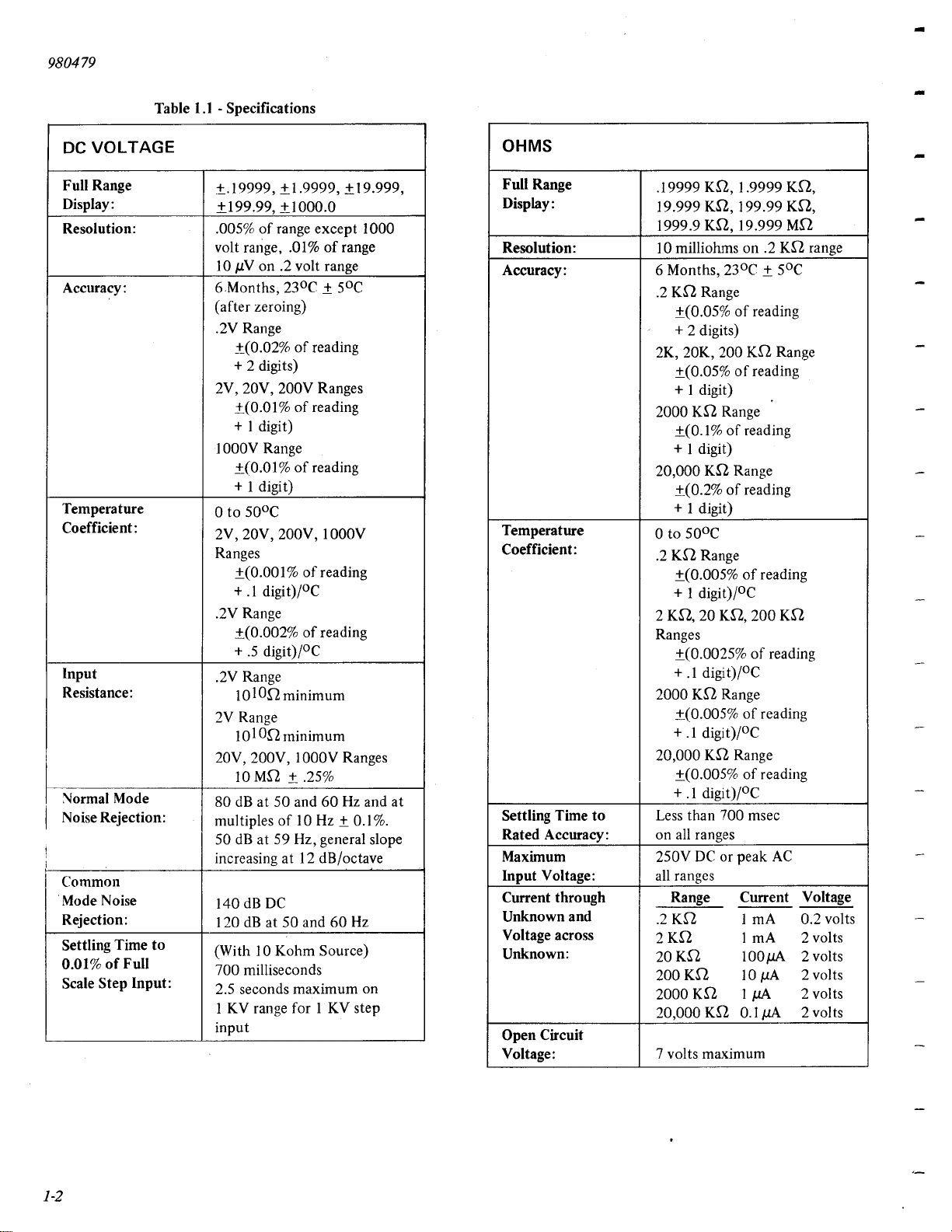
Specifications . 1-2
Front
Panel
Identification.
Rear
Panel Identification
Available
Maximum
Pin Location
Function
Range Codes
Serial
Serial
Parallel
Sequence Chart
KOhms Calibration
DC
AC
Resistance Calibration Adjustment
DCV Unit Performance
ACV
KOhms Unit Performance Test
ACmA Unit Performance Test
Main
Main PCB, Null Detector Subassembly Performance Test 5-34
Main
Display Subassembly Performance Test 5-46
AC
Battery Pack
Table 7.1
List
Ranges.
Inputs.
J202
Codes
Out
Pin Location
Data
Out
Out
Pin Location
Check.
Calibration Adjustment
Calibration
Unit Performance Test
Unit Performance Test 5-16
PCB, Power Supply (Line Only) Subassembly Performance Test 5-21
Table
Table 5.15.2 5-21
Table 5.15.3
PCB, Reference Voltage Generator Subassembly Performance Test 5-24
PCB, Timing and Control Logic Subassembly Performance Test
PCB, Range and Relay Logic Subassembly Performance Test 5-30
PCB, Integrator Subassembly Performance Test .
PCB, Isolator/Bootstrap Subassembly Performance Test 5-40
Converter Subassembly Performance Test 5-53
Output
of
Suppliers .
S.15.1
(Opt.
(Opt.
Adjustment
Test
51)
Subassembly Performance Test
70) Subassembly Performance Test
Title
Test.
Page
2-2
2-3
24
2-4
34
3-4
3-4
3-4
3-5
3-5
4-12
5-2
5-3
5-4
5-4
54
5-5
5-7
5-7
5-7
5-10
5-12
5-14
5-18
5-21
5-21
5-21
5-22
5-26
5-38
544
5-56
5-63
7-1
7-1
vii
SECTION 1
ARTEKMEDIA => 2012
GENERAL DESCRIPTION
1.1
GENERAL.
1.1.1 The Dana Model 4600
curate, four digit instrument featuring auto range, auto
polarity, 80
mon mode noise rejection, and 10,000 megohm input
resistance on the
Available options include Battery Pack, Data Output, and
Read, Hold Probe.
1.1.2 The basic instrument has full multimeter capability
measuring full scale inputs from 10
five
DC
voltage ranges, from 10 mOhms to 20 Megohms on
ohms ranges, 10 namps to 2 amps on
ranges, and 10 namps to 2 amps on
1.1.3 High reliability
and solid-state circuitry, including the display. Protection
from possible introduction
through both mechanical and electrical means. The use
separate input terminals, while routing inputs only when
the proper function
nals reaching the wrong circuitry. The current functions are
protected on
function
rms
AC
handle inputs
20 kHz, decreasing to 200 volts at 100 kHz
dB
normal mode noise rejection, 140
DC
functions .2 and 2 volt ranges.
voltage ranges, from 10
is
is
selected, reduces the chance
all
ranges by a 2.5 amp fuse; the
is
designed to handle inputs
on
all
ranges; the
of
1000 volts
AC
is
a compact, highly
IN
J.J,V
to 1000 volts on
five
insured by the
of
fault voltage
of
volts function
DC
or 1000 volts rms
dB
com-
to 1000 volts on
five
five
AC
current
DC
current ranges.
use
of
LSI
MaS
is
provided
of
DC
volts
1000 volts
is
on
DC
designed to
AC
all
ranges.
ac-
AC
six
of
sig-
or
to
Option 84 RF Probe, measures RF voltages to
200
MHz.
Option 88
Option 89
1.2 MECHANICAL DESCRIPTION.
1.2.1 The basic
ment and comes equipped with a bail handle to simplify
carrying. The bail handle rotates 3600 and may be used
a "kickstand" for easy measuring and control access.
1.2.2
the power supply are mounted on two printed circuit
boards and housed
the interior
nance
1.3 ELECTRICAL DESCRIPTION.
1.3.1 The model 4600 utilizes the dual-slope integration
method
minimizes the number
ability and lower cost while having
stability and noise rejection.
All
is
made by removing three screws on the back panel.
of
Deluxe test leads, include assorted tips.
Standard test leads, with replaceable tips.
DMM
is
designed
components
of
the instrument for calibration and mainte-
analog-to-digital conversion. This technique
of
the basic instrument including
in
a high-impact plastic case. Access to
of
components for increased reli-
as
a bench top instru-
inher~nt
advantages
as
of
1.1.4 Also available
(designated 4600-51). The option provides the function,
range, polarity, and numeric readout data in
both serially and in parallel.
1.1.5 Accessories available for 4600 include:
Option
Option 70
Option 80
Option
Option 82
Option
61
81
83
is
the Option
Carrying case.
Battery pack for operation - up to
four hours continuous
where no
Shielded input cable, for use in high
noise environments.
Hold Probe, provides pushbutton control
of
5
measurement to 5
50
measurements to 50
AC
power
Measure/Hold functions.
KV
HV
Probe, extends
KV
HV
Probe, extends
51
Isolated Output
use
is
available.
KV.
KV.
BCD
in areas
DC
voltage
DC
voltage
form
1.3.2 The circuitry consists
section, digital section, and an analog-to-digital converter.
1.3.3 The analog-to-digital (A/D) converter changes a dc
signal fed into it into a representative digital signal. The
method used to perform this task
integration.
1.3.4 The digital section measures the
converter to produce a numeric value on the instrument
display that represents the value
digital section also provides range control and decimal
placement.
1.3.5 The signal conditioning section scales, filters, and,
when required, converts the input signal to a full scale
volts for the A/D converter.
1.4 SPECIFICATIONS.
1.4.1 Specifications are provided in table 1.1.
of
a signal conditioning
is
called dual-slope
output
of
the input signal. The
of
the
AID
±2
1-1
980479
ARTEKMEDIA => 2012
Table
1.1
- Specifications
..
DC
VOLTAGE
Full Range
Display:
Resolution: .005%
Accuracy:
Temperature
Coefficient:
Input
Resistance:
;\formal Mode
Noise Rejection:
I
!
I
Common
. Mode Noise
Rejection:
Settling Time to
0.01%
of
Full
Scale Step Input:
±.19999, ±1.9999, ±19.999,
+199.99,
volt range, .01%
10
6 Months, 230C ± 50C
(after zeroing)
.2V Range
2V,
1000V Range
+1000.0
of
range except 1000
of
J..LV
on .2 volt range
±(0.02%
+ 2 digits)
20V, 200V Ranges
HO.Ol %
+ 1 digit)
±(0.01 %
+ 1 digit)
of
reading
of
reading
of
reading
range
o to 50°C
2V, 20V, 200V, 1000V
Ranges
±(O.OO
1 %
of
reading
.1
digit)/oC
+
.2V Range
±(0.002%
+
.5
.2V Range
1010nminimum
2V
Range
101 On
20V, 200V, 1000V
10
Mn
80
dB
multiples
50
dB
increasing at 12 dB/octave
140
dB
120
dB
(With
10 Kohm Source)
700 milliseconds
2.5 seconds maximum on
1 KV range for 1 KV step
input
of
reading
digit)/oC
minimum
Ranges
± .25%
at 50 and
at 59 Hz, general slope
DC
at 50 and
of
10
60
Hz
±
60
Hz
Hz
and at
0.1
%.
OHMS
Full Range
Display:
Resolution:
Accuracy:
Temperature
Coefficient:
Settling Time
Rated Accuracy: on
Maximum
Input Voltage:
Current through
Unknown and
Voltage across
Unknown:
Open Circuit
Voltage: 7 volts maximum
to
.19999
19.999
1999.9
10
6 Months,
.2
2K,
2000
20,000
o to 50°C
.2
2
Ranges
2000
20,000
Less than 700 msec
2S0V
all
.2
2Kn
20Kn
200Kn
2000
20,000
Kn,
1.9999
Kn,
199.99
Kn,
19.999
milliohms on .2
230C ± 5°C
Kn
Range
±(O.OS%
+ 2 digits)
20K, 200
±(O.OS%
+ 1 digit)
±(
+ 1 digit)
±(0.2%
+ 1 digit)
Kn
±(O.OOS%
+ 1 digit)/oC
Kn,
±(0.002S%
.1
+
±(O.OOS%
.1
+
±(O.OOS%
+
.1
all
ranges
Range
Kn
Kn
Range
0.1 % of
Kn
of
Range
20
Kn,
digit)/oC
Kn
Range
digit)/oC
Kn
digit)/oC
ranges
DC
or peak
Kn
Kn
of
Kn
of
reading
Range
reading
of
of
Range
of
Current
1
1
100pA 2 volts
10
IpA
0.1
reading
reading
200
of
rnA
rnA
Kn,
Kn,
Mn
Kn
Range
reading
Kn
reading
reading
reading
AC
J..lA
pA
range
Voltage
0.2 volts
2 volts
2 volts
2 volts
2 volts
1-2
Table
ARTEKMEDIA => 2012
1.1
. Specifications continued
980479
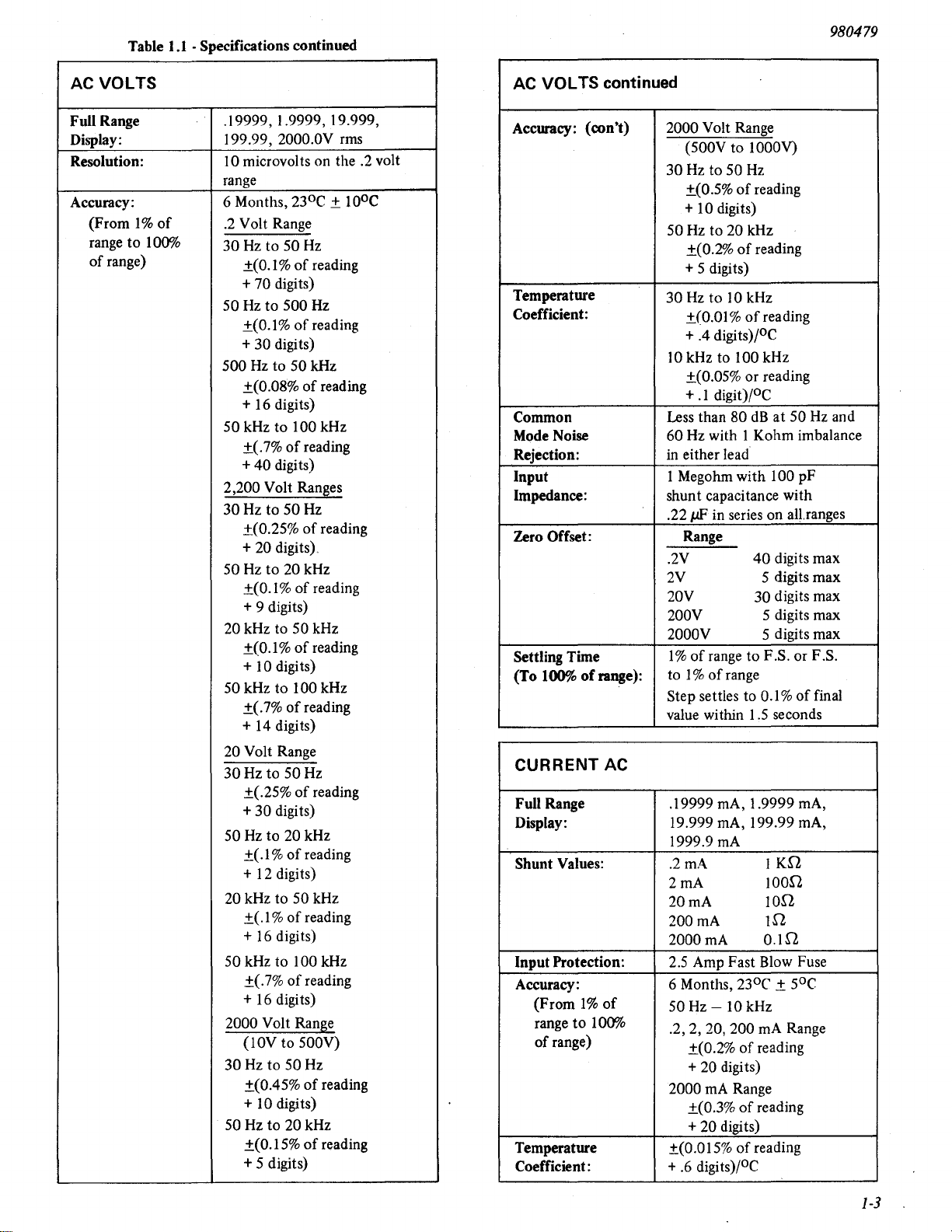
ACVOLTS
Full Range
Display:
Resolution:
Accuracy:
(From
1%
to
range
of
range)
of
100%
.19999, 1.9999, 19.999,
199.99,
10 microvolts on the .2 volt
range
6 Months,
.2
30
2000.0V rms
230C ± 100C
Volt Range
Hz
to 50
±(0.1 %
of
Hz
reading
+ 70 digits)
Hz
to 500
50
±(0.1 %
Hz
of
reading
+ 30 digits)
500
Hz
to 50 kHz
±(0.08%
of
reading
+ 16 digits)
50 kHz to
±(.7%
+
2,200
30
Hz to 50
±(0.25%
100 kHz
of
reading
40
digits)
Volt Ranges
Hz
of
reading
+ 20 digits).
Hz
to 20 kHz
50
of
±(0.1 %
reading
+ 9 digits)
20 kHz to 50 kHz
of
±(0.1 %
reading
+ 10 digits)
50 kHz to
±(.7%
100 kHz
of
reading
+ 14 digits)
20
Volt Range
30
Hz to 50
±(.25%
+
50
Hz
±(.1 %
30
Hz
of
reading
digits)
to 20 kHz
of
reading
+ 12 digits)
20 kHz to 50 kHz
±(.I % of
+
16
50 kHz to 100 kHz
±(.7%
reading
digits)
of
reading
+ 16 digits)
2000 Volt Range
(10V to 500V)
30
Hz
to 50
Hz
±(0.45%
of
reading
+ 10 digits)
50 Hz to 20 kHz
±(0.15%
of
reading
+ 5 digits)
AC VOLTS continued
Accuracy: (con't)
2000 Volt Range
(500V to 1000V)
30
Hz
to 50
±(0.5%
of
+ 10 digits)
50 Hz to 20 kHz
±(0.2%
of
+ 5 digits)
Temperature
Coefficient:
30
Hz
to
±CO.Ol
10
%
of
+ .4 digits)/oC
10 kHz to 100 kHz
±(0.05% or reading
+.1
digit)/oC
Common
Mode Noise
Rejection: in either lead
Input
Impedance:
Zero Offset:
Settling Time
(To 100%
of
range):
Less than 80
60 Hz with I Kohm imbalance
1 Megohm with 100 pF
shunt capacitance with
.221J.F
in series on aRranges
Range
.2V
2V 5 digits max
20V
200V
2000V 5 digits max
of
range to F
1 %
of
to 1 %
Step settles to 0.1 %
value within 1.5 seconds
range
CURRENT AC
Full Range
Display:
Shunt Values: .2
Input Protection:
Accuracy:
(From
1%
of
range
to
100%
of
range)
.19999 rnA, 1.9999 rnA,
19.999 rnA, 199.99 rnA,
1999.9
2mA
20mA
200
2000
2.5 Amp Fast Blow Fuse
6 Months,
50
.2,2,
rnA
rnA
rnA
rnA
Hz
- 10 kHz
20, 200
±(0.2%
23
of
+ 20 digits)
2000
rnA
Range
±(0.3%
of
+ 20 digits)
Temperature
Coefficient: + .6 digits)/oC
±(0.015%
of
Hz
reading
reading
kHz
reading
dB
at
50
40
digits max
30
digits max
5 digits max
.S.
or F
of
IKn
loon
Ion
In
O.ln
0
('
±
SoC
rnA
Range
reading
reading
reading
Hz
.S.
final
and
1-3
980479
ARTEKMEDIA => 2012
Table
1.1
- Specifications continued
•
-
CURRENT
Full Range
Display:
Shunt
Values: .2
Protection:
Input
Accuracy:
Temperature
Coefficient:
DC
GENERAL
±.19999 rnA, ±1.9999 rnA, Ranging:
±19.999
+1999.9
2mA
20
200 rnA
2000 rnA
2.5 Amp Fast Blow Fuse
6 Months,
.2, 2,
2000
o to
±(0.01 %
+ .2 digits)/oC
rnA, ±199.99 rnA,
rnA
rnA
rnA
230C ±
20, 200
±(0.12%
+ 4 digits)
±(0.3%
+
20 digits)
500C
rnA
of
Range
of
of
reading
IKn
lOOn
IOn
In
o.ln
SoC
rnA
Ranges
reading
reading
Digitizing
Technique: Dual Slope
Signal Integration Time:
Read Rate:
Maximum
Common
Mode Voltage:
Power
Requirements:
Storage
Temperature:
Operating
Temperature:
Warmup: 30 minutes
Weight
(Approx.):
Dimensions:
Automatic or Manual
100 msec ± .25%
400 msec per reading
2-1
/2 reading per second
+.25%
KV
DC
1
to Earth Ground
100, 120, 220, 240
±IO% from nominal.
50 to 400 Hz,
maximum
-200 C to
-200 C to 650 C w/battery opt.
0-
to 6 month accuracy
Std:
With Battery Option:
73mm x
(2.87 x 7.87 x 9.84 inches)
or peak
50°C
Kg
2.3
3.2
(Sibs.)
Kg
(7Ibs.)
200mm x 250mm
10
750 C
AC
volts
watts
input
1-4
SECTION 2
ARTEKMEDIA => 2012
INSTALLATION & OPERATION.
2.1
GENERAL.
2.1.1 This section covers the incoming inspection, instal·
lation, storage and operation
of
the Model 4600
DMM.
2.2 UNPACKING & INSPECTION.
2.2.1 The Model 4600
is
enclosed between two molded,
plastic·foam forms and packaged in a double·walled card·
board carton for shipment. The plastic forms hold the
instrument securely in the carton and absorb any reason·
able external shock normally encountered in transit.
2.2.2 Prior to unpacking, examine the exterior
shipping carton for any
the
DMM
from the carton and inspect the exterior
instrument for any
signs
signs
of
of
damage. Carefully remove
damage.
If
damage
of
is
found,
of
the
the
notify the carrier immediately.
2.3
BENCH
OPERATION.
2.3.1 The instrument comes equipped with a bail handle"
that doubles
elevating the front
as
a carrying handle and
of
the instrument.
as
a "kickstand" for
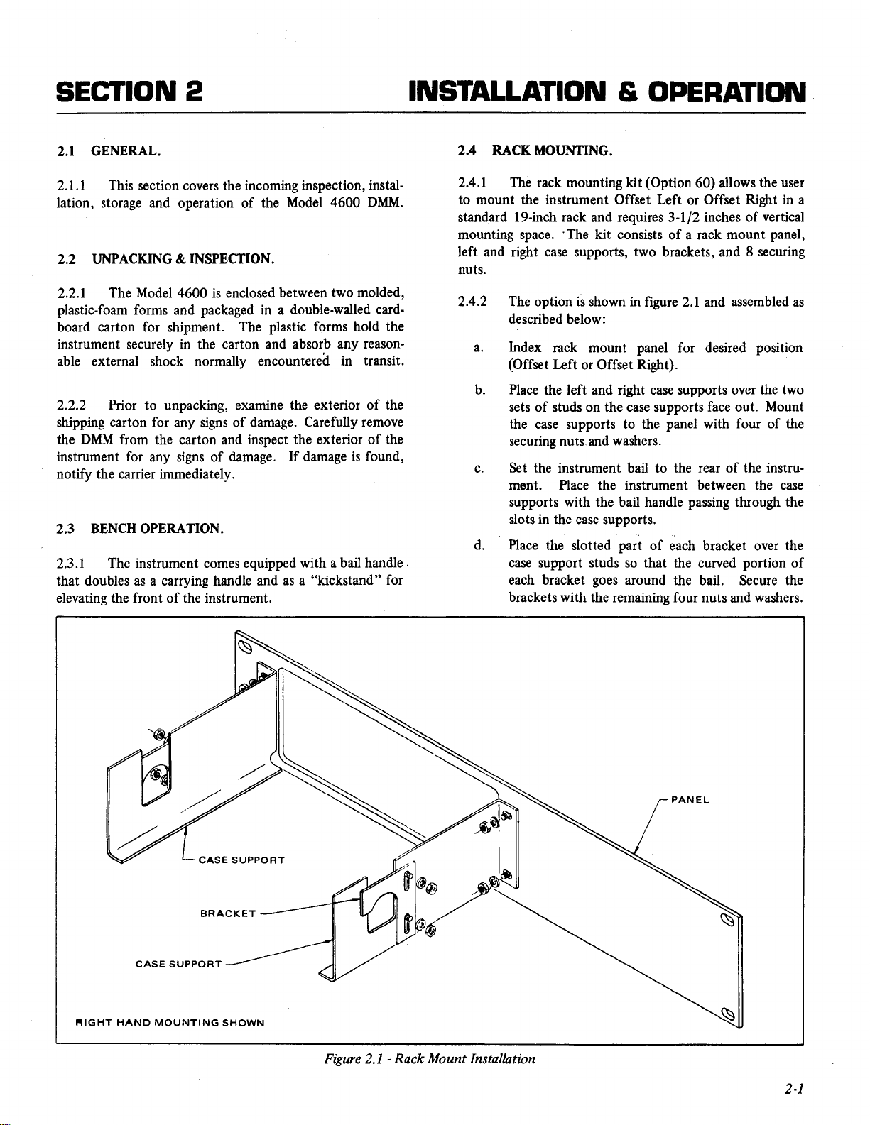
2.4 RACK MOUNTING.
2.4.1 The rack mounting kit (Option 60) allows the user
to mount the instrument Offset Left or Offset Right in a
standard 19-inch rack and requires 3-1/2 inches
mounting space.
left and right
"The
kit consists
case
supports, two brackets, and 8 securing
of
a rack mount panel,
of
vertical
nuts.
2.4.2 The option
is
shown in figure
2.1
and assembled
as
described below:
a.
Index rack mount panel for desired position
(Offset Left or Offset Right).
b. Place the left and right case supports over the two
sets
of
studs on the case supports face out. Mount
the
case
supports to the panel with four
of
the
securing nuts. and washers.
c.
Set the instrument bail to the rear
ment. Place the instrument between the
of
the instru·
case
supports with the bail handle passing through the
slots in the
d.
Place the slotted part
case
case
supports.
support studs
of
each bracket over the
so
that the curved portion
of
each bracket goes around the bail. Secure the
brackets with the remaining four nuts and washers.
RIGHT
CASE
HAND
CASE
SUPPORT
MOUNTING
SUPPORT
BRACKET
SHOWN
Figure 2.1 .
Rack
Mount
Installation
r-
PANEL
2-1
980479
ARTEKMEDIA => 2012
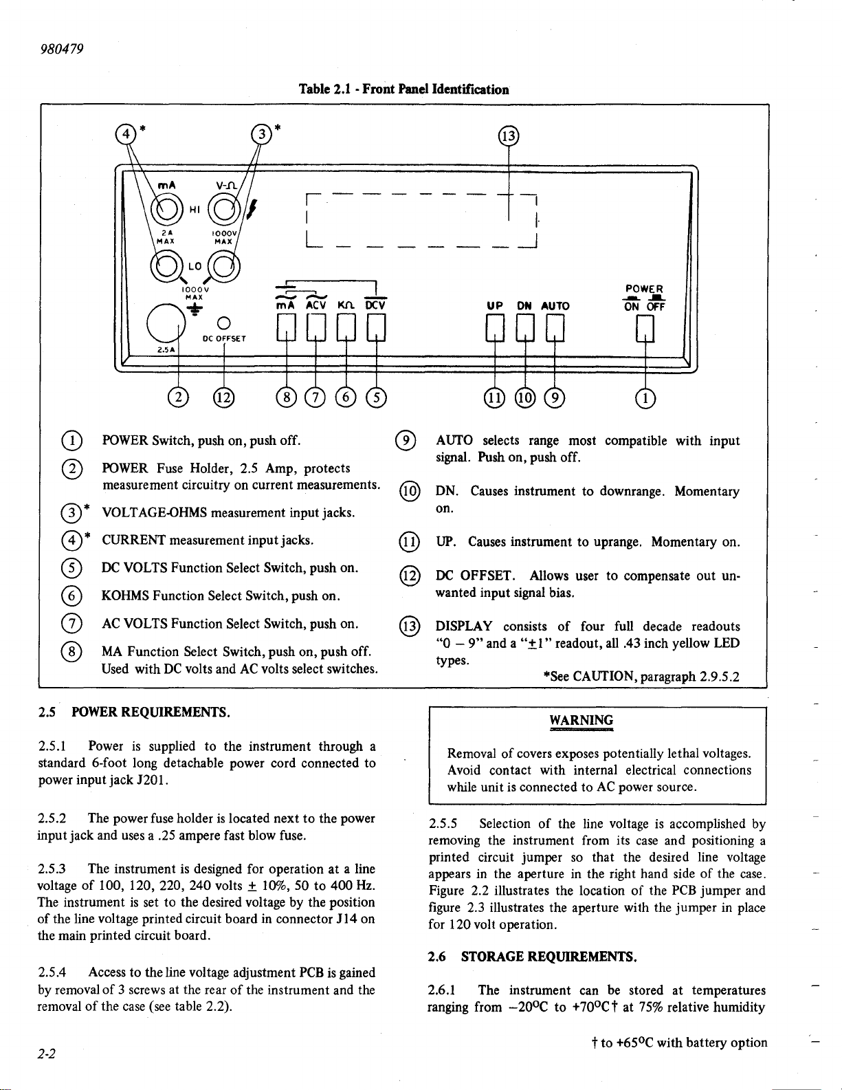
Table
2.1
-Front
Panel
Identification
13
CD
CD
0*
8)*
CD
(0
1-
- - -
I
L
POWER Switch, push on, push off.
POWER Fuse Holder, 2.5 Amp, protects
measurement circuitry on current measurements.
VOLTAGE-OHMS measurement input jacks.
CURRENT measurement
DC
VOLTS Function Select Switch, push on.
KOHMS Function Select Switch, push on.
input
jacks.
--
-I
I·
.-J
UP
ON
AUTO
AUTO selects range most compatible with
®
signal. Push on, push off.
DN.
Causes instrument
on.
UP.
@
@
Causes instrument
DC
OFFSET. Allows user
wanted input signal bias.
to
downrange. Momentary
to
uprange. Momentary on.
to
POWER
--.
......
ON
OFF
compensate
out
input
un-
AC
(j)
®
2.5
POWER REQUIREMENTS.
2.5.1
standard 6-foot long detachable power cord connected
power input
2.5.2 The power fuse holder
input jack and uses a .25 ampere fast blow fuse.
2.5.3 The instrument is designed for operation
voltage
The instrument
of
the main printed circuit board.
2.5.4 Access
by removal
removal
of
the line voltage printed circuit board in connector 114 on
VOLTS Function Select Switch, push on.
MA
Function Select Switch, push on, push off.
Used with
Power
jack
100, 120, 220, 240 volts ± 10%, 50
of
3 screws at the rear
of
the case (see table 2.2).
DC
volts and
is
supplied
1201.
is
set
to
the desired voltage by the position
to
the line voltage adjustment
AC
to
the instrument through a
is
located
of
the instrument and the
volts select switches.
next
to
the power
to
PCB
is
at
a line
400
gained
to
Hz.
DISPLA Y consists
@
"0 -9"
types.
2.5.5
removing the instrument from its case and positioning a
printed circuit jumper
appears in the aperture in the right hand side
Figure 2.2 illustrates the location
figure 2.3 illustrates the aperture with the jumper in place
for
2.6
2.6.1 The instrument can be stored
ranging from
and a
Removal
Avoid contact with internal electrical connections
while unit
120 volt operation.
STORAGE REQUIREMENTS.
of
is
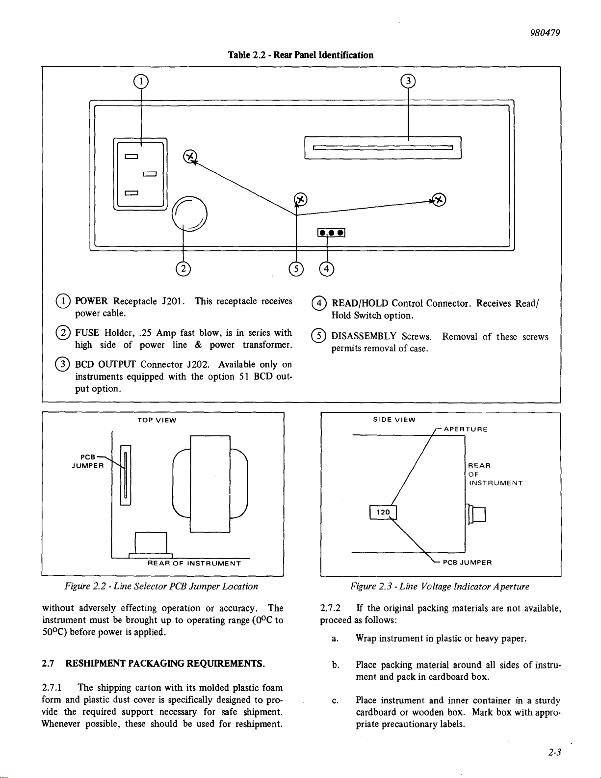
Selection
-200C
of
four full decade readouts
"±1"
readout, all .43 inch yellow LED
*See CAUTION, paragraph 2.9.5.2
WARNING
covers exposes potentially lethal voltages.
connected
of
to
AC
power source.
the line voltage is accomplished by
so
that
the desired line voltage
of
the
PCB
at
temperatures
to
+700Ct
at
75%
relative humidity
of
the case.
jumper and
2-2
t
to
+650C with battery option
CD
ARTEKMEDIA => 2012
POWER
power cable.
Table
2.2 -
Rear
c::::J
Receptacle 1201. This receptacle receives
Panel
Identification
8)
980479
3
READ/HOLD Control Connector. Receives Read/
Hold
Switch option.
CD
FUSE Holder, .25 Amp fast blow, is in series with
of
high side
CD
BCD
OUTPUT Connector 1202. Available only on
instruments equipped with the option
put
option.
Figure 2.2 - Line Selector PCB Jumper Location
without adversely effecting operation or accuracy. The
instrument must be brought
50°C) before power is applied.
power line & power transformer.
51
BCD
out-
TOP
VIEW
REAR
OF
INSTRUMENT
up
to
operating range
(OOC
to
eD
DISASSEMBLY Screws. Removal
permits removal
Figure 2.3 - Line Voltage Indicator Aperture
If
2.7.2
proceed
a. Wrap instrument in plastic or heavy paper.
the original packing materials are
as
follows:
SIDE
of
VIEW
case.
APERTURE
REAR
OF
INSTRUMENT
PCB
JUMPER
of
these screws
not
available,
2.7
RESHIPMENT
2.7.1 The shipping carton with its molded plastic foam
form and plastic dust cover
vide the required support necessary for safe shipment.
Whenever possible, these should be used for reshipment.
PACKAGING
is
specifically designed
REQUIREMENTS.
to
pro-
b.
Place packing material around all sides
ment
and pack in cardboard box.
c.
Place instrument and inner container in a sturdy
cardboard or wooden box. Mark
priate precautionary labels.
box
of
instru-
with appro-
2-3
980479
ARTEKMEDIA => 2012
INPUT jOUTPUT jCONTROLS.
2.8
2.8.1 In tables
controls and their function. Also described are input and
output connectors.
2.9
OPERA
2.9.1 Operation consists
tion, selecting autorange or manually selecting the desired
range, applying the input signal and reading the results on
the instrument readout.
2.9.2 Autorange.
nON.
2.1
and 2.2 are described the operating
of
selecting the desired func-
2.9.4.2 Overrange
the read rate.
2.9.5 Signal Input.
2.9.5.1 Signal input
front panel. These jacks accept standard probe banana
plugs and are spaced to accept dual banana plugs. Several
probe sets for the
Section 1).
2.9.5.2 The left hand pair
DC
and
AC
current measurements; the jacks on the right are
for voltage and resistance measurements.
is
indicated by the display flashing at
is
through four banana jacks on the
4600 are available from the factory (see
of
input jacks are reserved for
2.9.2.1 In autorange the instrument automatically selects
the range most appropriate for the signal being measured.
2.9.2.2
ranges
downranging occurs at
2.9.3 Manual Range.
2.9.3.1 When autorange
in manual range. Higher or lower ranges are selected by
pressing the
selected at the read rate within the range limits
selected function
pressed.
2.9.3.2 The available ranges for each function are given in
table 2.3.
As
the input signal changes, the instrument changes
as
required. Upranging occurs at 100%
5%
of
range.
is
not selected, the instrument
UP
or
DN
range buttons. A new range
as
long
as
the
UP
or
Table 2.3 - Available Ranges
DCI
DCV
.2
2 2 2
20
200 200 200 200
(rnA)
.2
20 20 20
ACV
.2
ACI
(rnA)
.2
DN
2
of
range and
of
the
buttons are
Kn
.2
2
20
200
is
is
CAUTION
Do not connect test leads between the
jacks. Application
these jacks can damage the instrument.
As
2.9.5.3
side
measured and the
ground.
be
tied
function. The shield then should be tied to the
input side.
2.9.5.4 Maximum inputs are shown in table 2.4.
Current
Volts
Volts
Kohms
Common
Mode
a general rule for voltage measurements, the
is
connected
If
shielding
to
the
LO
Table 2.4 -Maximum Inputs
Max
DC
AC
DC,
1000V
linearily to
250 volts max.
1000 volts
input to earth ground, data
mon tied to earth ground
of
voltage or current between
to
the highest impedance point
LO
side
is
connected to the point nearest
is
used on the input cables, it should
input side unless it
current input 2 Amps (current jacks)
rms
AC
1000 volts
DC
to 20
kHz
200V at 100 kHz
DC
or peak
rnA
is
used in the Ohms
rms decreasing
AC
max. from
output
and
LO
Von
to
current
com-
Hi
be
1000 2000 1000 2000
-
2.9.4 Overrange.
2.9.4.1 Overrange occurs when the signal being monitored
is
greater than the instrument can measure with the range
selected.
2-4
- -
2000
- 20,000
2.9.6 Function Select.
2.9.6.1 The select buttons for
volts are interlocked; when one
any other button in the set
2.9.6.2 The current button
AC
volt or
unselected when current measurement
DC
volt button for current measurement and
AC
volts, kilohms, and
of
these buttons
is
released.
is
selected in addition to the
is
pushed,
is
no longer desired.
DC
is
2.10
ARTEKMEDIA => 2012
HOLD/READ PROBE
2.1
0.1
This option consists
switch that connects to
2.10.2
With
the option plug inserted in 1203
position, the instrument takes readings only
switch
is
held down.
2.10.3. With the option plug inserted in
position, the instrument
switch
is
pressed.
2.11 BCD OUTPUT
(Option
(Option
n03
on the rear panel.
81).
of
a probe with a built-in
n03
goes
into the hold mode when the
51).
as
in
the read
long
in
the hold
as
the
2.11.1 This option provides function, range, polarity, and
value
in
BCD
the display
operated device.
quiring serial or parallel output. The option
detail
in
Section 3.
form for printer or other digitally
It
is
designed to interface with units
is
covered
re-
in
980479
to four hours
the instrument
power switch
2.12.2
level, the condition
of
continuous
is
connected to the power
is
set to the OFF position.
When
the battery charge drops below operating
is
use.
indicated
Recharging occurs when
by
a LED lamp on the
line
and the
instrument front panel. To fully recharge the batteries
quires about
Option 70
Option
16
hours.
NOTE
is
not available for units equipped with the
51
BCD Output.
re-
NOTE
Option
51
is
not available for units equipped with the
Option 70 battery pack.
2.12
BATIERVPACK(Option70).
2.1.2.1 With the battery pack option the instrument
becomes completely portable, taking measurements for up
CAUTION
On
units equipped for battery pack operation (Option
70)
the batteries
connected to the
ment
is
turned off. The batteries charge
mately
16
are
hours; it
charging when the instrument
AC
power source and the instru·
in
approxi·
is
recommended that the unit
is
be
unplugged during extended periods of non-use to
avoid
pOSSible
damage to the batteries.
2-5

THIS
ARTEKMEDIA => 2012
PAGE
LEFT
BLANK
SCANS
By
ArtekMedia

SECTION 3
ARTEKMEDIA => 2012
3.1
GENERAL.
Model
3.1.1 The
vides
the function, range, polarity, and numeric readout
data in
single
data
of
characteristics
3.2
3.2.1
printed circuit board that
BCD
connector on the instrument rear panel. The output
is
completely isolated from the measurement portion
the 4600, thereby preserving the common mode noise
MECHANICAL
All
components for the option
4600 Option
form, both serially and in parallel, from a
of
the instrument.
DESCRIPTION.
is
51
Isolated Output pro·
are
on a
mounted above the instrument
single
BCD OUTPUT
main
PC
board by four spacers;
located between the boards, prevents any digital
generated on the option board from affecting the measure·
ment circuitry on the
3.2.2
nector that extends out the back
a slot provided for this purpose. This connector
option output connector and
3.3
3.3.1 The option, shown in simplified block diagram
form in figure 3.1, consists
section, and six optical couplers.
One end
ELECTRICAL DESCRIPTION.
Main
board.
of
the option board forms an edge con·
is
of
a floating section, a grounded
an
aluminum shield,
of
the instrument through
designated J202.
J202
noise
is
the
Kn
RANGE
,
NUMERIC
DATA
TRANSFER
00
CLOCK
-100
AC
T
I
I
P7
I
:
I
I
1
I
I
I
I
I
I
:
1
FUNCTION
ENCODE
CONTROL
LOGIC
h>
:>
:>
MUX
f
r--
.-.-
......-
~
I
I
I
I
'-
OCll
I
I
OCI
I
I
I
OCI
I
I
I
OCI
I
I
I
I
10CIs
SERIAL
SERIAL
SERIAL
SERIALS
1 I
2 I
4 I
"-
I
SERIES
DATA
,
1
I
I
I
SHIFT
REGISTER
2
I
I
I
PARALLEL
OUTPUT
I
3
4
i
TIO
GEN
I
I
I
I
I
PARALLEL
1
OUTPUT
I
INHIBIT
I
SERIAL
STROBE
_I
HOLD~(~I----------------------------------~
FLOATING
SECTION
Figure
3.1·BCD
:
oc,.I"'~------------------------«
Hc5"i:D
I
I
Output
GROUNDED
SECTION
3-]
980479
ARTEKMEDIA => 2012
TRANSFER
00
"
L
COUNTER
U1
i
F/F
U5,U3
DATA
TRANS
DECODE
U5
GATE
U2,
U3
f--
~
PART
MUX
U6,U7
...
-
OF
MUX
SERIAL
DATA
CLOCK
DATA
CLOCK
(1
kHz)
TRANSFER
TRANSFER
(1
STROBE
Figure
~END
OF
.-J
00
_________
kHz)
I I
1
MS
I I
r
3.2 - Control Logic
DIGITIZING
t+--5
=il
--'I
.....
If-----
II
I I I I I I I I
MSEC--+j
n
8
MS
..
______
-----
_
...
~oIL
20
IlS
3-2
PARALLEL
DATA
VALID
Figure
3.3-
UNITS
TENS
HUNDREDS
Timing
THOUSANDS
TEN
THOUSANDS
FUNCTION-----..J
RANGE-------..J
Diagram
980479
ARTEKMEDIA => 2012
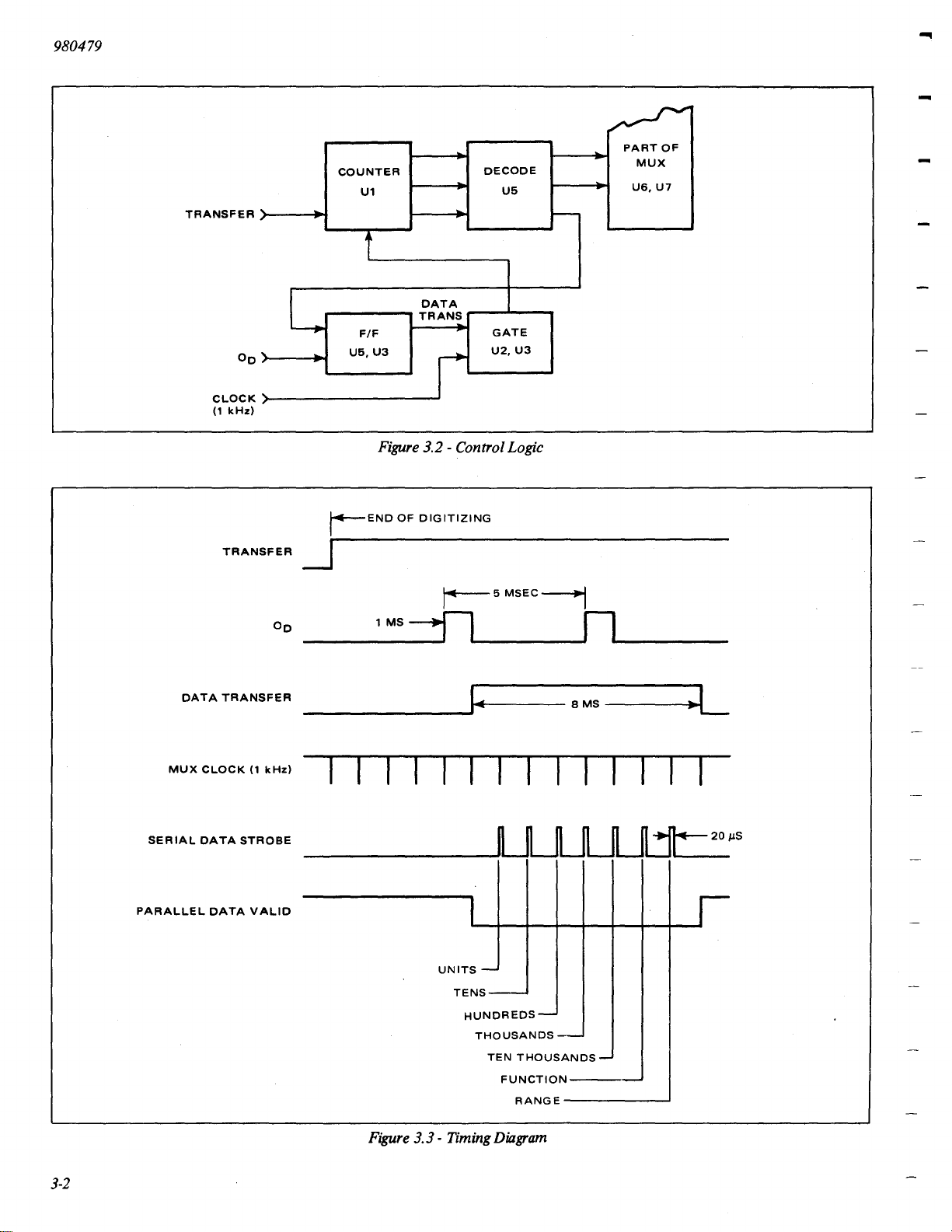
3.3.2 The floating section encodes and multiplexes the
binary data from the measurement portion
and transmits the data through optical couplers 1 through
5.
The sixth coupler
The floating section consists of: Function Encode, the
Multiplexer (MUX), and the
3.3.2.1 The multiplexer consists
line data selector/multiplexers,
receives inputs from the function encode circuitry and
trol signals from the control logic, both located on the option
board, and range and numeric data from the display board.
The
multiplexer has a 4-bit byte output which drives the
four optical data couplers; the output byte corresponds to
of
one
control logic.
3.3.2.2 The
consists
counter
generates the operational logic for the multiplexer and the
strobe
provides timing information for the grounded side. The
circuitry operates by following a predetermined series
steps shown in figure 3.3. The operation starts when the
TRANSFER line
as
OD,
Display board,
signal
data transfer signal enables the gate, allowing the 1 kHz
clock
board) to advance counter
is
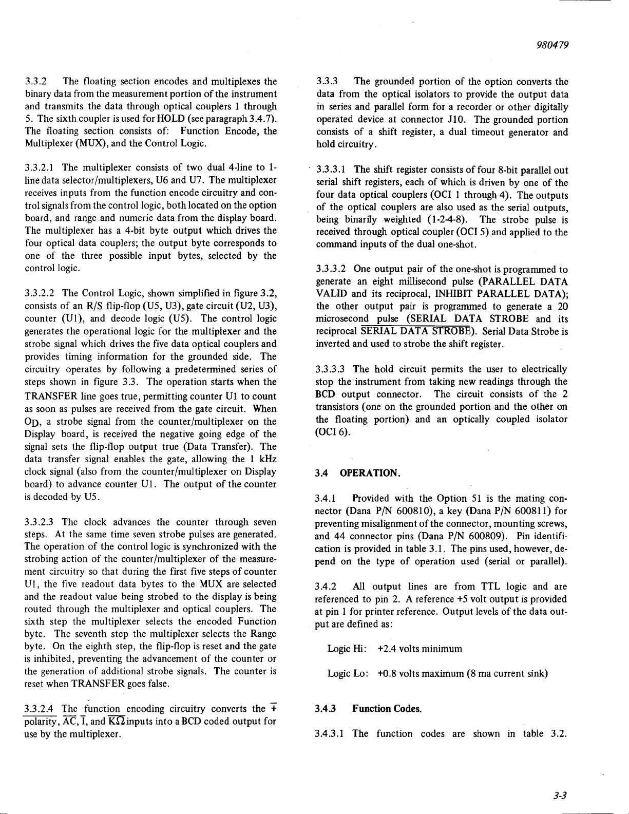
3.3.2.3 The clock advances the counter through seven
steps. At the
The
strobing action
ment circuitry
UI,
and the readout value being strobed to the display
routed through the multiplexer and optical couplers. The
sixth step the multiplexer selects the encoded Function
byte. The seventh step the multiplexer selects the Range
byte.
is
the generation
reset when TRANSFER
the three possible input bytes, selected by the
Control Logic, shown simplified in figure 3.2,
of
an R/S flip-flop (US, U3), gate circuit (U2, U3),
(UI),
signal
which drives the
soon
as
pulses
a strobe
sets the flip-flop output true (Data Transfer). The
signal
(also from the counter/multiplexer on Display
decoded by
operation
the
five
readout data bytes to the
On
the eighth step, the flip-flop
inhibited, preventing the advancement
is
used for
and decode logic (US). The control logic
goes
true, permitting counter Ul to count
are
received from the gate circuit.
signal
from the counter/multiplexer on the
is
received the negative going
US.
same
time seven strobe pulses are generated.
of
the control logic
of
the counter/multiplexer
so
that during the first
of
additional strobe signals. The counter
HOLD
Control Logic.
U6
five
Ul.
The output
goes
false.
of
and
data optical couplers and
is
of
the instrument
(see paragraph 3.4.7).
two dual 4-line to
U7.
The multiplexer
edge
of
the counter
synchronized with the
of
the measure-
five
steps
of
MUX
are selected
is
reset and the gate
of
the counter
1-
con-
of
When
of
the
counter
is
being
or
is
3.3.3 The grounded portion
data from the optical isolators to provide the output data
in
series and parallel form for a recorder or other digitally
operated device at connector
of
consists
hold circuitry.
3.3.3.1 The shift register consists
serial shift registers, each
four data optical couplers (OCI 1 through 4). The outputs
of
the optical couplers are also used
being binarily weighted (1-24-8). The strobe pulse
received through optical coupler (OCI 5) and applied to the
command inputs
3.3.3.2 One output pair
generate
VALID
the other output pair
microsecond pulse (SERIAL DATA STROBE and its
reciprocal
inverted and used to strobe the shift register.
3.3.3.3 The hold circuit permits the user to electrically
stop the instrument from taking new readings through the
BCD
transistors (one on the grounded portion and the other on
the floating portion) and an optically coupled isolator
(OCI6).
3.4 OPERATION.
3.4.1 Provided with the Option
nectOr
preventing misalignment
and 44 connector pins (Dana PIN 600809). Pin identification
pend on the type
3.4.2
referenced to pin
at pin 1 for printer reference.
put
are defined
Logic
Logic
a shift register, a dual timeout generator and
of
the dual one-shot.
an
eight millisecond pulse (PARALLEL
and its reciprocal, INHIBIT PARALLEL DATA);
is
SERIAL DATA STROBE). Serial Data Strobe
output connector. The circuit consists
(Dana
PIN
600810), a key (Dana PIN 600811) for
of
is
provided in table 3.1. The pins used, however,
of
operation used (serial or parallel).
All
output lines are from TTL logic and are
2.
A reference
as:
Hi:
+2.4 volts minimum
Lo: +0.8 volts maximum (8
of
the option converts the
110. The grounded portion
of
four 8-bit parallel out
of
which
is
driven by one
as
the serial outputs,
of
the one-shot
programmed to generate a 20
the connector, mounting screws,
+5
Output
is
programmed to
51
is
the mating con-
volt output
levels
of
rna
current sink)
of
DATA
of
the 2
is
provided
the data out-
the
de-
is
is
3.3.2.4 The function encoding circuitry converts the
polarity,
use
AC,
T,
and
Kn
by the multiplexer.
inputs into a
BCD
coded output for
+"
3.4.3
3.4.3.1 The function codes are shown
Function Codes.
in
table 3.2.
3-3
980479
ARTEKMEDIA => 2012
Table 3.1 - Pin Location
1202
+5V
Ref
Earth Ground
Output
Serial
Thousands (4)
Function
Range (4)
Hundreds (4)
Tens (4)
Units (4) 14 R
Serial
Output
Thousands (1)
10 Thousands
Function (1) 18 V Function
Range (1) 19 W Range
Tens (1)
Hundreds (1)
Units (1)
I
Function
-DC
+DC
ACV 1 1 0 0 3
-DCI
+DCI
ACI
Kn
3.4.4 Range Codes.
3.4.4.1 The range codes are shown in table
(4)
(4)
(2)
(1)
Table 3.2 -
Fl
0
1
0 0
1
1 1 1 0
1
A
1
B
2
3
C
D
4
E Serial Data Strobe
5
F
6
7 H Hold
J Serial
8
K
9
10 L
11
M
12 N
P Tens (8)
13
15
S
16
T
17
U
20 X
Y Tens (2)
21
22 Z
Function
F2
0
0
0
0
J202
Serial Data Strobe
Parallel
Inhibit
Thousands (8)
+ Polarity
Hundreds (8)
Units
Serial
. Thousands
10 Thousands
Hundreds
Units (2)
Data
Parallel
Output
(8)
Output
(2)
(2)
(2)
(2)
Codes
F4
0 0 0
0 0 1
1
1 0 5
0 1
F8
0
3.3.
Valid
Data
(8)
(2)
(2)
(OL)
Dec
4
7
9
Table
3.3
Range
20,000 1
2,000 0 0
200 1
20
2
.2
3.4.5 Serial
3.4.5.1 The data
lines; strobe data
form.
vided in table 3.4.
Pin identification for lines used in serial
+5V
Ref
Earth Ground 2
Output
Serial
Output
Serial
Rl
0
1
0 0
Output.
output
is
available in logic true and inverted true
Table
3.4
- Serial
(4
lines) 8
(2
lines)
-Range Codes
R2
0
1 0 3
1
0 0
is
available in serial form
Out
1202
1 A
R4 Dec
1 5
1 4
0 2
0 0
Pin Location
B
3 C
4 D
5
6
7
9
10
11
12
13
14
15
16
17
18 V
19
20
21
22
Serial Data Strobe
E
Serial Data Strobe
F
H Hold
Serial
J
Output
K
L
M
N
P
R
Serial
S
T
U
W
X
Output
Y
Z
out
(8
(2
1
on
four
is
pro-
lines)
lines)
3-4
3.4.5.2 At the completion
ARTEKMEDIA => 2012
strobe
output
rate. During each strobe pulse, a new data byte appears
the data
Word
1 8 4 2
2
3
4
5 0 0
6
7 0
3.4.6 Parallel Output.
3.4.6.1 The data
(parallel) on twenty-four lines
3.4.6.2 Data
Data pin D is true
the inverted
true logic
3.4.7 Hold.
3.4.7.1 The hold line
held at logic low, prevents a new measurement cycle from
starting. Any measurement in progress when hold
manded
generates seven 20
output
is
lines. The serial data is shown in table 3.5.
Table 3.5 - Serial Data
8 4 2
80
800
8K 4K 2K
F8
is
at
the
output
(8
output
is
required for a print pulse.
allowed
of
to
complete.
of
the measurement, the data
J1Second
Bit
40
400
F4 F2
R4
available in standard
of
1202
pins is available when Parallel
milliseconds). Inhibit Parallel Data is
pin D and can be used when negative
is
an external command line. When
pulses at a 1 kHz
Out
20
200
20K(OL)
R2
BCD
as
shown in table 3.6.
1
1
10
100
lK
10K
Fl
Rl
is
at
form
com-
Table 3.6 -Parallel Out Pin Location
1202
+5VRef
Earth Ground
Thousands (4)
Function (4)
Range (4)
Hundreds (4)
Tens (4)
Units (4)
Thousands (1)
10 Thousands (1) 17 U
Function (1)
Range
(1)
Tens (1)
Hundreds (1)
Units (1)
3.4.7.2 The value
display and is available
(although no new parallel data
The data
following the last reading taken.
is
not present at the serial data
1 A
B
2
3
C
4 D Parallel Data Valid
E
5
F Inhibit Parallel Data
6
7 H Hold
J Thousands (8)
8
9 K
L
10
M
11
12
N Hundreds (8)
13
P Tens (8)
14 R
15
S
T Thousands (2)
16
18
V
19
W Range (2)
X Hundreds
20
Y Tens (2)
21
Z Units (2)
22
of
the last measurement remains in the
at
the parallel data
Units (8)
10
Thousands (2) (OL)
Function (2)
(2)
output
pulse
is
980479
output
output
lines
generated).
lines
3-5

THIS
ARTEKMEDIA => 2012
PAGE
LEFT
BLANK
SCANS
By
ArtekMedia
SECTION 4
ARTEKMEDIA => 2012
THEORY
OF
OPERATION
4.1 GENERAL.
of
output
the Model
as
well
as
is
pre-
level pro-
ac
4.2 This section describes the operation
4600
DMM
and includes the basic teclmique used
of
more detailed explanation
CIRCUIT DESCRIPTION.
4.3
4.4 A functional block diagram
sented in figure 4.1. The diagram
areas for purposes
(2) Digitizing, (3) Ranging, and (4) Display. Measurement
signals applied to the input terminals are routed to the
appropriate signal conditioning device by the function
controls. Because the isolator amplifier operates with low
voltages, dc measurement signals higher than 2 volts must
be
scaled down. This
The attenuator also changes the source current flow on the
ohms ranges and provides the required shunting on
current ranges. The
attenuator for the
4.5 The ac converter produces a dc
portional
the ac ranges this
to
of
ac
the ac measurement applied to its input. On
dc
the major functional portions.
of
the instrument
is
divided into four major
discussion;
is
accomplished by the attenuator.
converter contains its own voltage
ac
voltage ranges above 2 volts.
signal
(I)
Signal Conditioning,
is
applied to the isolator.
4.9 The Timing and Control circuits provide the integrator and counter with the synchronization required to
of
perform the analog to digital conversion
a
signal. The instrument performs continuous measurement
cycles. The measurement cycle
4.10 Note that the digitize cycle
major periods. The first, which
the signal integrate period. During this time the Timing and
Control circuits apply the measurement signal to the input
of
the integrator. The integrator, during this period,
charges a capacitor to a level determined by the value
measurement signal. During the next period the Timing
Control circuits apply a reference voltage opposite in
and
polarity to the measurement signal to this capacitor
order
to
discharge it. The capacitor
as
rate and
integrator produces a null detect signal which
the Timing and
measurement counter. Thus, the value
measurement counter
of
the measurement signal. During the signal integrate
period the Timing and
of
the measurement signal and store this information
flip-flop.
the charge on the capacitor reaches zero the
Control circuits to stop the count in
is
directly proportional to the value
Control circuits detect the polarity
is
is
the measurement
illustrated in figure 4.3.
is
divided
100 milliseconds long,
is
discharged at a fixed
of
in
is
used by
the count
to four
of
the
in
the'
in
the
in
is
a
4.6 The ohms amplifier produces a dc
portional
ranges. Like the
produced by the ohms amplifier
input.
4.7 The isolator functions
tion
to
the
put impedance on the low voltage dc ranges
ment. The
for conversion to a digital count.
4.8 The integrator
which charges a capacitor for a fixed time period to a level
which
(see figure 4.2). The capacitor
'rate by switching a reference signal
onto the input
charges it crosses the zero volt level and 'begins to charge
the opposite direction. A null detector in the integrator
circuit senses this zero-crossing and produces a
detect"
and
Thus, the count value in the measurement counter is a
direct digital representation
voltage applied to the instrument.
to
the direct current at its input on the ohms
ac
converter, the dc output voltage
is
as
a buffer to prevent applica-
of
"normal-mode" noise or "common-mode" voltages
integrator circuit.
output
is
dependent upon the level
signal. The null detect signal
Control circuits
of
of
It
also serves
the isolator
is
the integrator.
to
is
applied to the integrator
a dual-slope conversion device
of
is
then discharged at a fixed
stop the measurement counter.
of
the measurement signal
output
applied to the isolator
to
provide a high
the measuremen t signal
of
opposite polarity
As
the capacitor
is
used by the Timing
level pro-
of
the instru-
in-
dis-
"null-
in
4.11 The measurement counter
circuit chip which includes the measurement counter, a
latch to store the count, a decoder, and multiplexer. The
measurement count stored in the latch
be
must
LED
coder. The multiplexer,
transfers one digit
to the 4-to-7 line decoder. The 7-line
decoder
parallel. The
as
Thus, the
sequence but the display rate
the LEDs appear to
4.12 Range control
from the front panel or automatically by the internal range
control logic. There
of
operator desires to
pushes
it
switch
through
control logic configures the voltage attenuator and current
shunt to scale down measurement input signals. In
converted
display. This
is
applied to
its code appears on the
LED
the instrument labeled
in
the Auto pushbutton (a latching type switch) . .If
is
desired to use manual range control the Auto range
is
unlatched and the operator then has control
use
of
to
a 7-line code for application to the
is
accomplished by the 4-to-7 line
in
of
information at a time from the latch
all
of
MUX
switching line turns on each LED digit
output
display devices
be
continuously illuminated.
is
accomplished either manually
are
three switches on the front panel
UP,
use
the auto ranging feature he simply
the
UP
and
DOWN
is
a special integrated
is
in
BCD
code and
the measurement counter,
code from the
the
LED
display digits in
of
the 7-line decoder.
are
actually flashing in
is
of
a frequency that makes
DOWN,
and AUTO. If the
pushbuttons. The range
de-
4-1
SIGNAL CONDITIONING
ARTEKMEDIA => 2012
AC
CONVERTER
~".-t
t
•
MEASUREMENT
INPUT
TERMINALS
~
~
~
RANGE
REFERENCE
r------.,
INTEGRATOR
REFERENCE
GENERATOR
FUNCTION
CONTROLS
CONTROL
NULL
DETECT
....
VOLTAGE
\
--......
\
CONTROL
SIGNALS
~VOLTAGE~
ATTEN
l......a...
r-"""""
~
AND
CURRENT
SHUNT
1=======I=======lISOLATOR
~
f t
LATCH
4-LlNE
AND
MULTI
OHMS
AMP
LI
FIE
I
~
BCD
~
I
________________
I
I
I
R
r.o-
DECODER
~
1.",0..
MEASUREMENT
_---
TIMING
AND
CONTROL
START/
..
STOP
..--~
TIMING
SIGNALS
COUNTER,
DECODER
PLEXER
~----~--
L-~P~O~L=A~R~IT~Y~
MUX
4-TO-7
LINE
__
I--
SWITCHING
~-r~r-~---+---+---r/
~
~
LED
DISPLAY
I'
~
7·LlNE
I I
::ODE
4-2
____
I
RANGE RANGE RANGE
CONTROLS
L.........
,---.-
CO
NT
RO
LOGIC
L
Figure
DIC:T~IN~
:
~ISPLAY
__
_
RANGING
CODE
4.1 -Functiona I Block
DECIMAL
DECODER
CIRCUIT
AC~
OHMS~
DC
DECIMAL
1-
_______________
PATH
LEGEND
Diagram
POINT
...tL._...,.L-_...,.L-
__
-----L.
__
---'
ISOLATOR
ARTEKMEDIA => 2012
REFERENCE
GENERATOR
Figure 4.2 -Dual Slope Integration
I
SIGNAL
I
I
10,000
100
INTEGRATE
COUNTS
MSEC
REFERENCE
INTEGRATE
TO
10,000
100
COUNTS
MSEC
I
a.
J
1
I
I
a·2~--------------~
I
REFSW--
RESET
addition, it controls the attenuator in the
circuit, The isolator gain
control logic and
depending on the selected operating range
ment,
The range code from the range control logic
applied to the decimal decoder which provides the signals
to the
LED
______________
__________________
Figure 4.3 -Display Cycle Timing Using Dual Slope Integration Technique
is
is
switched from
displays
to
properly locate the decimal point,
~--------------~L--------------.-----~-I~------------------
r-
- - - - - - "'T - - - - - - -
:~
______________
AC
Converter
also controlled by the range
Xl
to
XIO gain,
of
the instru-
REFERENCE
INTEGRATE
TO
20,000
100
:~
____________
is
RESET
10,000
COUNTS
MS~C
100
COUNTS
MSEC
I
I
..
---------------i
__________
__
~I
4.13 Function Controls.
A simplified block diagram
illustrated
in
figure 4.4. The function controls consist
front panel pushbuttons labeled Milliamps,
Kohms, and
DC
Volts. Note that there are two sets
put terminals for applying measurement signal to the input
of
the function controls
AC
Volts,
of
in-
is
of
4-3
q
ARTEKMEDIA => 2012
HI
LO
DCV
ACV
Kn
--
0----,
~
rnA
ACV
S1
~
S2
---
-
AC
CONVERTER
--
AC/DC
rnA
>-
Kn
S3
1\
S4
of
input terminals
Figure
of
the instrument. One set
urement
terminals
of
ac and dc milliamps. The other set
is
used for measuring dc volts, ac volts and
DCV
4.4
-Function Controls
Kohms. The four function control switches route the
put measurement signal through one
ac
making
measurements
measurement signal
to
terminals
the input
of
either voltage or current. The
is
routed from either set
of
the
AC
of
Converter. When making
dc voltage or current measurements the measurement signal
is
applied to the input
of
the isolator and,
OHMSAMP
""-
ISOLATOR
is
for meas-
of
input
in-
three paths when
of
input
in
like fashion,
the ohms measurement signal
is
routed to the input
of
the
ohms amplifier. Although the block diagram shows that the
is
measurement signal
applied to the input
three circuits, measuremen t signals
of
one
are
actually routed
of
these
through the voltage attenuator and current shunt circuits
for pre scaling purposes. This
discussed in more detail
in
is
the following paragraph.
4.14 Voltage Attenuator and Current Shunt. This cir-
cuit
is
shown in simplified form in figure 4.5. The attenuator
and shunt circuit performs the following functions;
tenuation
of
input measurement voltages on the 20, 200,
1)
at-
and 1000 volt dc ranges, 2) scales down the ohms current
is
source when the instrument
as
3) acts
a shunt when on the
on the Kohms ranges,
ac
or dc current ranges, and
4) the attenuator and shunt circuit contains two series
resistance strings with pick-off
pOints selected by range
lays. In figure 4.5 the left-hand resistance string
re-
is
the
voltage range attenuator and ohms current source divider.
as
The right-hand resistance string serves
the ac and dc current shunt, and also has pick-off points selected by range
relays. In the upper left-hand corner
that the dc measurement signal
of
figure 4.5 note
is
switched around the
attenuator on the low ranges and goes directly to the
isolator.
On the 20, 200, and 1000 volt ranges the
measurement signal
is
switched onto the top
of
dc
the range
DC--.()--
RANGE
RANGE
20.,200,1000
SELECTED
ATTENUATION
S3-8
.2
8.
2.
,---------
'------__.--(100
RELAY
POINTS
RANGE
":"10
•
-'-100
• (10J.LA
.!-1000
•
1MA
Kn
TO
ATTENUATOR
nA
(1
J.LA
Kn
(100
J.LA
KnSOURCE
0--+1
V
ISO
(10
Kn
SOURCE)
SOURCE)
KnSOURCE)
Kn
SOURCE)
(OHMS
REFERENCE)
Mnl
DCV
RANGE
DVDR
(ATTN)
AC/DC
.2
2
20
200
CURRENT
rnA
rnA
rnA
rnA
2A
Kn
RANGE
DIV
(SOURCE
SHUNT
m
RELAY
SELECTED
SHUNT
POINTS
AC/DC
rnA
CURRENT
SHUNT
44
M
Figure 4.5 - Voltage Attenuator and Current Shunt
Kn
ARTEKMEDIA => 2012
IN
Kn
PUT_
........
/V\..-
+15V
>----1
OUTPUT
OUTPUT
PROTECTION
CLAMP
DRIVE
Kn
Figure 4.6 - Ohms Amplifier
attenuator resistance string. On these ranges the isolator
connected to the appropriate point on the range attenuator
resistance string for pre scaling.
When
4.15
the instrument
current, the measurement
is
used to measure
signal
is
ac
applied to the top
or dc
of
the
right-hand resistance string, the ac/dc current shunt. The
range
relays then select the appropriate pick-off point
the shunt resistance string and apply that signal to the
put
of
the isolator.
in
in-
is
4.16
S3,
When
the instrument
in
the lower left corner
is
used to measure resistance,
of
figure 4.5,
is
switched to the
Kohm position and the range relays pickoff the appropriate
point to apply,
amplifier. Configuration
thus accomplished by accommodation
control setting
as
a current source, to the input
of
the attenuator and shunt
an~
the
s~ate-of-the-range
of
the function
relays.
of
the ohms
is
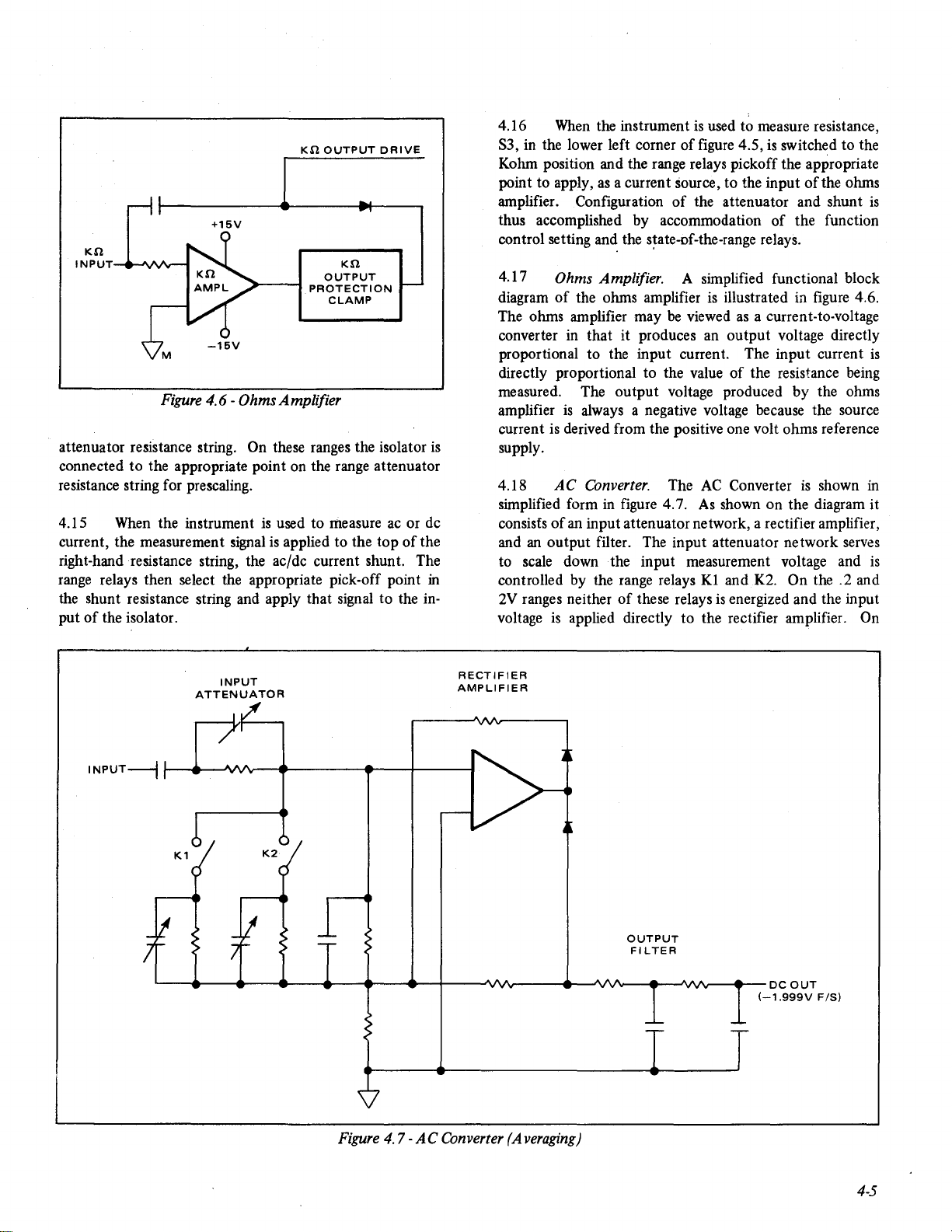
4.17 Ohms Amplifier. A simplified functional block
of
diagram
The ohms amplifier may
converter in that it produces
proportional to the input current. The input current
directly proportional to the
the ohms amplifier is illustrated in figure 4.6.
be
viewed
value
as
a current-to-voltage
an
output voltage directly
of
the resistance being
is
measured. The output voltage produced by the ohms
amplifier
current
is
always a negative voltage because the source
is
derived from the positive one volt ohms reference
supply.
4.18
simplified form
consists
and
to
controlled by the range relays
2V
voltage
AC
Converter. The
in
figure 4.7.
of
an
input attenuator network, a rectifier amplifier,
an
output filter. The input attenuator network
scale
down the input measurement voltage and
ranges neither
is
applied directly to the rectifier amplifier. On
of
these relays
AC
Converter
As
shown on the diagram it
K1
and
K2.
is
energized and the input
is
shown
in
serves
is
On the .2 and
INPUT
ATTENUATOR
INPUT---1r--4~~AAr--4~------
K1
~--~--~~--~--~~--~--
__
~--+-----~
RECTIFIER
AMPLIFIER
OUTPUT
FI L TER
__
~~----~Ar-----e--JV~---e--JVVV--~---DCOUT
(-1.999V
F/S)
Figure 4.7
-AC
Converter (Averaging)
4-5
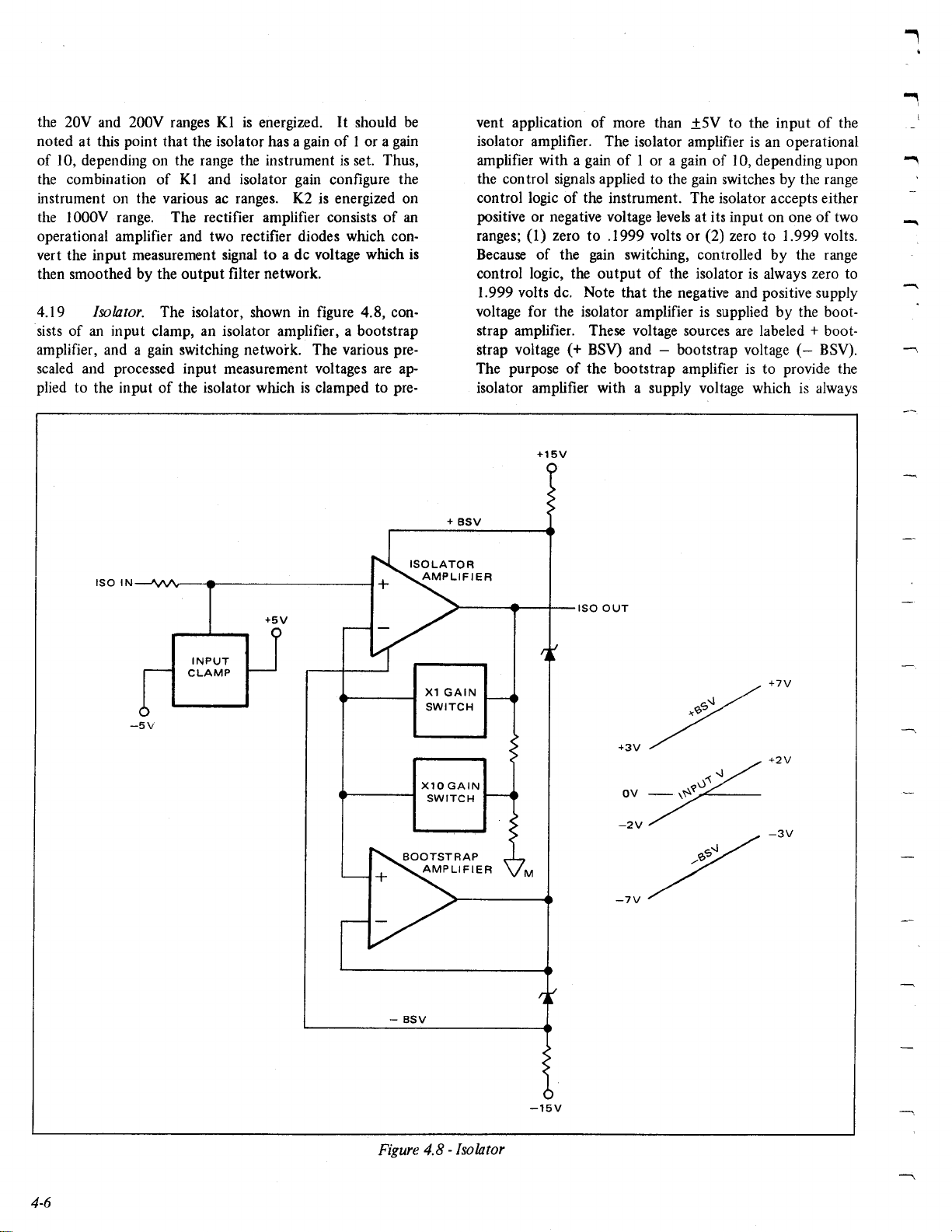
i
ARTEKMEDIA => 2012
the 20V and 200V ranges
noted at this point that the isolator has a gain
of
10, depending on the range the instrument
the combination
of
instrument on the various
the
lOOOV
range. The rectifier amplifier consists
Kl
is
energized. I t should
of
1 or a gain
is
set. Thus,
be
KI and isolator gain configure the
ac
ranges. K2 is energized on
of
an
operational amplifier and two rectifier diodes which convert the input measurement signal
then smoothed by the
output
to
a dc voltage which
filter network.
4.19 Isolator. The isolator, shown in figure 4.8, con-
sists
of
an
input clamp, an isolator amplifier, a bootstrap
are
pre-
ap-
amplifier, and a gain switching network. The various
scaled and processed input measurement voltages
plied to the input
of
the isolator which
is
clamped to pre-
vent application
isolator amplifier. The isolator amplifier
amplifier with a gain
of
more than
of
±5V
1 or a gain
to the input
is
an operational
of
10, depending upon
of
the
the control signals applied to the gain switches by the range
control logic
positive or negative voltage levels at its input on one
ranges;
is
Because
control logic, the
of
the instrument. The isolator accepts either
(1) zero
of
to
.1999 volts
or
(2) zero to 1.999 volts.
the gain switching, controlled by the range
output
of
the isolator
is
always zero to
of
two
1.999 volts dc. Note that the negative and positive supply
is
voltage for the isolator amplifier
strap amplifier. These voltage sources
supplied by the boot-
are
labeled + boot-
strap voltage (+ BSV) and - bootstrap voltage (-BSV).
of
The purpose
isolator amplifier with a supply voltage which
+15V
+
BSV
the bootstrap amplifier is to provide the
is
always
ISOIN--~~--~----------------~
+5V
INPUT
CLAMP
-5V
....
-------1
>---
X1
GAIN
SWITCH
X10
GAIN
SW
ITC
-
BSV
....
---+---ISO
H
OUT
+7V
s..J
~<O
/
+3V
.",,?vy+2V
OV_~_\tA'?V
_2V/_
-7V
/<0
s..J
3V
4-6
-15V
Figure 4.8 -Isolator

SLOPE
ARTEKMEDIA => 2012
CAPACITOR
FROM
ISOLATOR
FROM
-
REF
FROM
+
REF
AMP
AMP
SIGNAL
SWITCH
-
REF
SWITCH
+
REF
SWITCH
1--e~Mrl"'-~
RESET
SW
1--
.....
------1
RESET
SW
Figure 4.9 -Integrator
centered about the input measurement signal to the isolator
amplifier. The
the input signal and the -
+
BSV
voltage
BSV
is
always 5 volts higher than
is
always 5 volts lower than
the input signal voltage. Thus, the isolator amplifier
always supplied with source voltages centered around the
input signal. This combination provides high input imped-
. ance to avoid loading the circuit under test.
4.20 Integrator. The integrator
performs the analog-to-digital conversion
ment signal and
is
illustrated in figure 4.9. The integrator
is
the circuit which
of
the measure-
uses the dual slope integration technique to perform the
analog-to-digital conversion. Refer to figure 4.3 for the
cycle timing relationships that relate to the dual slope
of
integration. During the reset portion
the measurement
cycle the two reset switches close placing the offset
of
capacitor across the output
This charges the offset capacitor
offset voltage that appears at the
detector amplifier. At the beginning
of
grate portion
the measurement cycle the reset switches
the null detector amplifier.
toa
level equal to any
output
of
of
the signal inte-
the null
open and the signal switch closes, thus placing the offset
capacitor in series with the measurement signal from the
at
isolator
the input
positive or negative offset voltage
from the signal being measured. The output
of
the integrator amplifier. Thus a
is
added to or subtracted
of
the inte-
. grator amplifier charges the slope capacitor for a fixed
of
period
the capacitor
time (100 milliseconds). The charge placed on
is
dependent on the magnitude or level
of
the
measurement signal from the isolator. Refer to figure 4.3,
note that there are two slopes shown representing the
capacitor charging slope; these represent two measurement
is
levels. Note that the time
the same for the charge for
NULL
DETECT
FEED
FWD
SWITCH
M
both measurements
charge level
is
signal integrate period
is
charging rate and level
measurement
but
that the charging rate and the final
different. From this it can
is
always the same length but the
of
the capacitor varies with the
Signal.
At the end
of
the signal integrate
be
period the feed forward switch adds a small amount
OUT
seen that the
of
charge to the capacitor to make up for a slight delay which
is
incorporated to allow similar lines and circuits to settle
out between the reference integrate and signal integrate
of
portions
the measurement cycle. This causes the slope
capacitor charge voltage to increase slightly. At the
beginning
the reference integrate period
of
the measure-
of
ment cycle the signal switch opens and either the - refer-
ence switch or the
reference voltage to the input
in
opposite
polarity to the voltage
nal previously applied. This reference voltage
+ reference switch closes to apply a
of
the integrator amplifier
of
the measurement
is
sig-
applied to
the integrator amplifier and causes the slope capacitor to
discharge
a fixed rate.
When
the slope capacitor reaches
at
the zero level the null detector amplifier produces a null
detect pulse. Note
ments the rate
the
same
angle. Also note that for different measurement
that
of
discharge
in figure 4.3 that for
was
the same, e.g., the slope
both
measure-
is
signals input the zero crossing occurs at a different point in
be
time. Thus, it can
seen that the time periods
reference integrate portion
proportional to the value
of
output
the null detector
of
the measurement cycle
of
the measurement signal. The
is
used by the Timing and
of
the
is
Control circuits to stop the measurement counter. On
figure 4.3 the
Qe
1 and
Qe 2 Signals
shown are timing signals
generated by the measurement counter chip and used by
the Timing and
and generation
Control circuits for circuit synchronization
of
control
Signals.
4-7

+15V
ARTEKMEDIA => 2012
~6.4V
>---i
>--.4
-1V
.....
+1V
.....
-TO
-TO
-
+
REF
REF
-
-
SWITCH
SWITCH
Figure
4.10 -
4.21
the source
integrator and
ment at the voltage attenuator and current shunt circuit.
The reference generator
reference device
operated at its zero temperature coefficient current.
produces approximately 6.4V.
this 6.4V
provides the reference input to three operational amplifiers.
The
calculated to cause
the - reference source. The other two 1
fiers
meters which are adjusted to provide
reference source. These two amplifiers are operated at
unity gain,
output.
Reference
of
is
applied across a voltage divider network which
-1
V reference amplifier
are
connected to a voltage divider through potentio-
Generator.
the + and - reference voltage used by the
of
the + 1 V source used for ohms measure·
is
a selected high stability
it
to produce exactly
The reference generator
is
illustrated in figure 4.10. The
:z;ener
As
shown in figure 4.10,
is
configured with feedback
-IV
dc output for
V reference ampli·
+ 1 V dc from the
are
non-inverting, and produce a positive 1 V dc
is
diode
It
+1V
>-~.--
Ref~rence
Generator
4.22
is
controlled by the Timing and Control circuits (figure 4.11,
block diagram). These circuits provide synchronization and
control signals which control the sequence
referred to
the measurement cycle timing. Note that the timing
forms
and polarities for a positive measurement signal while the
lower portion illustrates the negative input example.
The differences between the upper and lower portions
the figure are the polarity
slope and polarity, the timing
switch and reset switch. The following description
operation
simplified block diagram (figure 4.11) and the timing chart
(figure 4.12).
TO
Timing
as
the measurement cycle. Figure 4.12 illustrates
in
the upper portion
of
the timing and control circuits refers to the
Kf1
SWITCH/ATTENUATOR
and
Control
Circuit.
of
of
the input signal, the integrator
.
Operation
the figure illustrate timing
of
signal switch, reference
of
the 4600
of
operation
wave-
of
of
the
4-8

1
ARTEKMEDIA => 2012
~
V
(OVERRANGE)
+5V
+5V..!!..
11
12
11
2-
.,....
+ N D
-
3
..
U11
D
CLK
CLR
113
N.D.
U12
D
CLK
CLR
POLF/F
U12
D
CLK
F/F
Q
F/F
Q~
13
Q
Q
ARM·RESET
B
GATE
9
--
10,":::
U1~~
P-Q
-
~6
7
~4
3
/
5
~
/'
12
INTERNAL
RESET
5
~
3
4
U13
~
6
U9
11
~
,...
~TORNGSW
6
fr,
U14
11
,
~"G'NT
MEASUREMEN
CYCLE
RESET
(INTEG)
RESET
(UPRANGE)
OIL'
(DISPLAY
OIL
10
-
REF
(INTEG)
(INTEG)
TIMIN
SW
PCB)
SW
T
G
S
W
RESET
2
u
U9
1
,....
SIG
INT
~
-
2
U13 U14
13
13
ft.7-
9
U7
+
SIG
(AUTO
REF
(INTEG)
INT
RANGE
SW
~
5
'--
~
U9
4
~
~
~
r-
9
~
/"
POL
DR
F/F
US
2
'--
D
3
CLK
Q
1
U7
~
LO
= -
POL
HI
= +
6
POL
RESET
(AUTO
+
TR
RANGE)
POL
ANSFER
Figure 4.11 - Timing and Control Circuit, Simplified
Block
Diagram
4-9

-
ARTEKMEDIA => 2012
-
EXAMPLE:
RESET--t
INTEGRATOR
NULL
DETECTOR
TRANSFER
-
RESETSW'I
+1.0000V
OUT
DC
SIGNAL
INTEGRATE
10,000
100
I
Qe1-.J
I
Qe2
SiGiNT-,
I
I
--.J
I
I
RESET
....J
I
I
SIG
SW....J
I
REF
SW
I
I
SIGNAL -2.V
~REFERENCE
COUNTS
MSEC
DC
RANGE
INTEGRATE
(HIS)
100
10,000
MSEC
(HIS)
INPUT
:tREFERENCE~RESET~SIG.
COUNTS
INTEGRATE
(F/S)
10,000
100
COUNTS
MSEC
10,000
100
COUNTS
MSEC
I
I
L
I
I
I
I
I
I
L
I
I
,-
I
I
r
I
I
I
I
I
L
INT.
4-10
Figure 4.12 -Measurement Timing Cycle

EXAMPLE:
ARTEKMEDIA => 2012
-1.9999V
DC
SIG
2.V
DC
RANGE
(F/S
INPUT)
INTEGRATOR
NULL
DETECTOR
TRANSFER..-J
RESETSW
RESET-nSIGNALrl:REFERENCE:tREFERENCE~RESET~SIG'
10,000
I
I
INTEGRATE
COUNTS
100
MSEC
(HIS)
~+8V
INTEGRATE
10,000
COUNTS
100
MSEC
INTEGRATE
(F/S)
10,000
100
COUNTS
MSEC
10000
'100
COUNTS
MSEC
I I
I I
I I
I
INT.
I I I I
I I I I
I I I
I
I
OUT
I
I
O~
81
0
---1
082
SIG
INT---,
I
I
I
I I
I
I
I
I
I
r
I
I
r
I
I
I
I
L
I
I
I
RESET
SIGSW
+
REF
SW
I
I
---1
I
I
~
I
I
I
I
I
I
I
I
r
I
I
I
I
I
I
I
I
L
Figure 4.12 -Measurement Timing Cycle continued
4-11

Table 4.1 -Sequence Chart
ARTEKMEDIA => 2012
-
+ Signal =
Qe 1
Qel
Qel
I.OOOOV
= High, Q
= Low, Q
= High, Qe2 = Low
2 = High
e
2 = Low
e
DC,
2.
Range
SIG
(1)
(2)
(3) - N.D.
(4)
(5) INTERNAL RESET goes low (caused by 2, 3, 4)
(6)
(7)
(8)
(9)
(10) POL
(1)
(2)
(3) - REF
(1) NUlL DETECTOR OUTPUT goes high (zero detect)
(2)
(3) INTERNAL
(4)
(5) - REF
(6)
INT goes low
+ N.D.
FIF
(Ull)
Q goes high
F/F
(Ul2)
<1
goes high
RESET goes high
TRANSFER goes high (Armed for digitizing sequence)
RESET
SIG
NULL DETECTOR OUTPUT goes low
POL F
SIG
SIG
+ N.D. F
TRANSFER goes low (signals
RESET
SW
goes low (releases sw's from Auto Zero)
SW
goes high (connects iso out
FIF
Q OUTPUT goes high (to enable - ref
IF
Q OUTPUT goes low (set pol dr F
INT goes high
SW
goes low (disconnects iso out from integrator in)
SW
goes high (connects
IF
(Ull)
Q goes low (causes internal reset to
RESET goes high (causes transfer to
SW
goes low (disconnects
SW
goes high (closes
to
integrator in)
(to
detect polarity)
IF
-1
V ref to integrator in)
CMOS
counter to stop count)
-IV
ref from integrator in)
rc::set
switches - Auto Zero)
Q
sw
output
go
@refint)
high)
go
high)
low)
(1)
Qel
= Low, Q
In
addition
in table 4.1. This chart
operation
urement cycle. Its basic purpose
reading the detailed description presented in the following
paragraphs.
while reading the detailed description.
Four timing segments
3814 counter, on the Display
frequency
exactly
output
The timing sequences are
Qe
Q
to
the illustrations, a sequence chart
of
the timing and control circuits for one meas-
It
will also serve
.of 100 kHz, these four timing sequences are
100 msec in duration. They are established by the
of
the last cOunter bit (1/2 decade), Qel and Qe2.
1 =
1,
Q
2 = 1
e
100 msec, count from 30,000 to 39,999 called
Signal Integrate
l = 0, Qe2 = 0
e
100 msec, count from 00,000 to 09,999 called
reference integrate. This count total limit
to
as
half-scale
2 = High
e
is
a syt'lopsis
as
a handy reference
are
established by the
PCB.
as
follows:
is
of
the sequence
is
for reference after
CMOS.
With an internal clock
RESET
presented
to
use
chip,
is
referred
of
SW
is
high (Auto Zero)
Q
1 =
1,
Q
e
100 msec, count from 10,000 to 19,999 called
reference integrate. This count total limit
to
= 0, Qe2 = 1
Qe 1
100 msec,
(fixed)
In the following example, a
to the isolator amplifier input. The isolator,
has
an output voltage
grate period
integrator input, resulting in a negative going slope, to
approximately
The null detector input senses the negative integrator slope
voltage and causes the null detector
negative TTL level. The null detector low
inverted through UlO and applied to Ul2-2, the D input
the polarity F
logic low, which when applied to the D input
drive F
IF,
to annunciate the
2 = 0
e
as
full-scale
countfrom
of
is
detected, this + 1.0V dc
-4.0V
IF.
U8-2, causes the Q
at the end
This causes UI2-6, the Q
"plus" symbol on the readout.
20,000 to 29,999 called reset
+ 1.0V dc input signal
at
+ 1.0V dc.
output,
When
the signal inte-
is
applied to the
of
the 100 msec period.
output
U8-6 to
to
output
of
the polarity
be
is
referred
is
applied
a gain
of
go
output
to be
logic high
1,
to a
is
of
4-12

At the start
ARTEKMEDIA => 2012
V9-3, signal integrate, goes logic low. This logic level
applied to the "clear" inputs, pin 13,
This causes the Q outputs
which
. respectively. Signal integrate at a logic low causes the out-
put
of
pin
11
be
at logic low and when inverted through
output at pin 8 to be logic high. This signal
transfer. When the start
must
crossing (null detect) occurs the falling edge
nals the
terminated and transferred to the latches for multiplexing
to the readout segments in digit sized bytes.
When
digitize sequence,
lateral signal switch,
to the integrator input,
ramp in a negative slope for a period
At the start
pin
8 goes low; this
that drives the reset bi-Iateral switches, V16B and
release the integrator from the reset state called
Zero."
At the end
when inverted through V14, disables the signal
switch, disconnecting the integrator input from the isolator
output.
polarity F
V13
pin 8
applies logic high levels to the three inputs
output
the
drives the
a
-l.OV
quence called reference integrate, whose purpose
the integrator
is
zero
high state; which, when inverted through VIO,
level
at the clock input, pin
Detect F
output
inverted, causes the reset bi-lateral switches,
VI6C, to close; placing the integrator
called
also
causes the transfer to
termination
of
the signal integrate sequence, the
of
VII
of
Ull
and V12 to go logic high,
is
applied to the inputs
V9-6 to
input
go
CMOS
signal integrate
detected, the
IF,
of
"Auto Zero." The inverted
go
logic high, which
of
V13, which results
of
to a logic high (ARMED),
3814 counter that the
is
at a low state, at the beginning
it
is
inverted through
VI6A,
that
of
signal integrate, when the
is
inverted through V 10-6 and V
of
signal integrate, V9-3 goes logic high, that
As
previously mentioned, the Q
IF,
V12-5
is
at a high state. Also the
is
logic low, which when inverted through
at pin 6
"-"
dc to the integrator input during the second
whose Q
V13 pin 8 to
of
to
go
logic low. This inverted output
reference bi-lateral switch, VI5C; connecting
output
signal back to a zero level. When the
output
output
go
go
the clock count
of
V13, pins 9 and 10
is
also applied
in
the
output
VI0
signal integrate occurs, transfer
so
that when a zero
of
BCD
count
V14
to drive the
to connect the isolator output
starts the integrator
of
output
output
of
V13, causing
of
the null detector changes to a
ca'.ls~s
11
of
VII,
of
the Plus Signal
goes logic low, causing the
logic high. This
to a logic low that signals the
in
output,
in
a configuration
output
of
the
CMOS
output
and V12.
to
the
V13-8 to
causes the
is
called
transfer
100 msec.
V16B and
V13 pin 8
is
to
of
output
of
VI3
14-4
VI6C,
"Auto
bi·lateral
of
output
VI0
is
to drive
a low
double
3814.
sig-
bi-
the
se-
of
be
to
to
of
3,
sensed, the next sequence, state
is
a
until sequence 4, which
If a null detect
1000 counts (5%
lowest range (in auto range) a down range
If a null detect
accumulated in the
ciated on the readout, flashing 20000, for a manual range
or highest range per function
is
and overload
one range. This
3814 counter, which
When null detect has
is
detected
logic high to detect
If
the input signal to the
inverted output
F
IF
"D"
pin 6 to
the Plus Reference
integrate. sequence two is entered and 2)
to the Polarity Drive F
be
logic low or minus polarity.
to
output
The
signal, goes to a logic low level when zero detect
this causes the
causing the transfer to
count.
4.23 Counter. The heart
Digital Voltmeter logic array, shown on figure
counter, latch,
detailed illustration
It
contains four full decade coun ters, two overflow latches,
an
underrange output,
drive a
puts to strobe the display. The 3814 counts four full digits
and the overrange digit. The
input to the 3814 chip. The decade counters change state
on
4.24 The
clock pulse to provide a divide-by-one hundred (
put. This clock pulse
3814 and a synchronous timing pulse for the data
programming operations. The step input clocks a ring
counter that drives the multiplexer.
BCD
the rising edge
sensed, the range counter,
as
the fixed reset period the Qe2L line goes
of
input at
be
logic low to
of
Q
4·1ine
to seven segment converter, and decoded out·
output
is
a fixed reset sequence.
is
sensed, during sequence state 2, before
of
range), and the
is
not
sensed before 19,999 counts
CMOS
is
a result
"overload" or
the null detector is applied to the polarity
VI2·2,
the null detector, for a negative input
output,
of
of
the clock pulse.
of
3814,
..
of
is
latched
not
been sensed and the
DMM
which now causes the Q output at
be
applied to
bi·lateral switch when the reference
IF
to cause the Q
pin 8
go
logic low, terminating the
of
decoder, and multiplexer. A more
this device
an
overrange output, outputs to
the second decade
is
used to drive the step input
is an "internal" reset
DMM
is
not on the
is
commanded.
an
"overload"
If the
DMM
the Qe2
100 kHz clock drives the
output
as
an
output
"up
range."
is
of
negative polarity, the
I)
Ul3-2 to enable
V8-2,
output
of
Ul2,
the instrument
is
shown
is
is
annun-
is
in auto range
V4
is
advanced
of
the
CMOS
called Qe2L.
4th
sequence
"D"
input
of
V8 pin 6
is
sensed,
to go logic low
CMOS
is
the 3814
4.1
as
in
figure 4.13.
gated with the
.;.
100)
of
outputl
is
the
CP
out·
the
At this point, the digitizing sequence
sequence 2,
is
only
at
the end
but
because a zero detect (null detect) has been
of
4.25 The 1
is
3814
buffered and used
output
of
the fourth decade counter in the
as
a
divide-by-t~o
thousand
4-13

-
ARTEKMEDIA => 2012
M
TRAN
4
~[>-
T TES
K
2
3
P
10 COUNT
PAUSE
P
C
1
2
S
SYNC
'}
+10
+100
120
19
-
A
-
)
A
--C
J J
B
3814
,.
-
C
~
)
0 E
f...-.......<:
';'4
DO
01
J
0--
~
[>-
{>
18
a
16
"0
E1
E2
BLN
12
o
~
OET
0 E
LATCH
Lc
f
Lc
I
f f
-C
f
P
3
K
BLANKING
CONTROL
ABC
6
SCANNER
j
17
21
22
7
8
111
STEP
-{)
4::
f
B
IA
: I
C SELECT
0
E
MULTOPLE,,"
02
°1
4
clo
03
5
9
a
{>
E
04
Vss
VGG_
VOO
10
6
E2L
2
1
1
4
5
3
4-14
Figure
4.13 - Logic Array

(
ARTEKMEDIA => 2012
.;-
2,000) output. This
that
is
less
than
enabled before the divide·by·2,000
output will signal the auto range circuitry
5%
output
of
full scale.
is
used
to
If
the transfer pulse
output
indicate a signal
goes high the
that
change must be made.
4.26 The
are
designated
step the
QO
and
Ql
flip.flop
as
Qe 1 and Qe2 outputs. These outputs
DMM through the various periods
outputs
of
the
5th
of
gration process. The signal codes are:
. Qe2
Qel
100
ms
- Signal integration - decade counts
from
30,000
to
39,999
o 0 100 ms - Reference integration - decade
counts from
00,000
to
9,999 H/S
o 100 ms - Reference integration - decade
counts from
o 100
ms
20,000
4.27 The Qe2
output.
If
output
a DMM uses a full scale count
the 3814, the high state
overrange condition. The Qe2L
to read
20,000 at a flashing rate.
10,000
to
19,999F/S
- Reset - decade counts from
to
299,999
is
latched and used
of
Qe2L is used
output
as
of
19,999 using
to
indicate an
causes the display
is
a range
counter
the inte·
the Qe2L
==
4.31 Qe 1
switch is turned
nected
to
0 and Qe 2
off
the input
switch. The decade counter
will ignore the
first
10 counts are ignored. This period allows for masking
next
==
O.
During this period the signal
and a reference (plus or minus)
of
the integrator through a bi·lateral
is
set
to
00,000 and the 3814
10 counts. Because
of
the 3814, the
is
con·
the noise at the time when the signal integration
switched
detection at or near zero analog
to
the reference integration
to
prevent
input
signals. The count
false
zero
started from 00,000 until the null detector crosses zero and
signals .the
detect signals the transfer input
end
of
the reference integration period. Zero
to
store the BCD count
of
the decade counters into the latches. If the transfer occurs
before the
5%
of
is
in
4.32
period is from
of
the
4.33
the analog and reference inputs to the integrator are
moved and bi·lateral switches short the integrator input
the
output
of
this period
.;-2000
full scale and a down range
au
to
range.
Qe
1
output
==
1 and Qe2
goes true, the signal is
is
commanded if the DMM
==
O.
This reference integration
10,000 to 19,999 which is the F /S capability
DMM.
Qe
1
==
0 and Qe2
==
1.
This is the reset period when
in a configuration called auto zero. The count
is
from 20,000
to
29,999. If the
less
than
reo
to
Qe2Loutput
goes true before zero detect signals a transfer, an uprange
commanded
detected and
if
the DMM
the
display indicates overrange.
is
in
auto range and/or overload
is
is
is
is
is
necessary
BCD
4.28 The edge sensitive transfer input causes the
data in the counters
to
be stored
in
the latches on the
falling edge. Synchronization with the clock
to prevent loading and storing erroneous counter states
at a
"carry"
command
is
trickling through the counters. A transfer
is
accepted once during an integration cycle.
An
internal flip·flop is reset by the counter transition from
39,999
remains set until the next integration sequence.
transfers will be accepted when this flip·flop
4.29 The clock pulse
counter. As previously mentioned the states
Qe2 control the state
to
00,000.
It
is set when a transfer occurs and
is
constantly adding counts
of
Qe 1 and
of
events
that
take place during an
is
to
No
set.
the
integration sequence.
4.30 Qe 1
30,000
this time the
amplified, converted, and/or filtered and connected
integrator input through a
ward circuit
the integrator
==
1 and Qe2
to
39,999. This
DMM input signal which has been attenuated,
of
the integrator adds 10 digits
output
==
1.
The counter advances from
is
the signal integration period. At
bi·lateral switch.
The
to mask the switching transients that
feed for-
of
voltage to
to
the
occur during the transitions from signal integrate to
reference integrate.
4.34 The step input from the
BCD
the multiplexed
decoder/driver, such
Oa
to
Oe
drive transistor circuitry
outputs
as
a SN7447. The decoded outputs
capable
output
of
driving a single
that
strobes the anodes
presents
.;-100
the display devices one at a time. .
4.35 4·to-7 Line Decoder. The 4-to·7 line decoder
shown on figure 4.14. This device
coder
that
converts
BCD
code
purposes. It's driven by the
counter chip and its
I
of
the display LEDs.
FROM
3814
Figure
BCD
2
4
7·line
output
...--
__
4.14
- 4-to-7 Line Decoder
is
simply a matrix de·
to
7·line code for display
BCD
code from the 3814
is
tied in parallel to all
...,
SEGMENT
a
b
c
TO
DISPLAY
LEOS
d
1
TO
e
9
5
of
is
4-15

FROM
ARTEKMEDIA => 2012
MUX
A
B
--~~--------------~~----------~~----------~------------~
C
D
E
DC
I
?
?
__________
__
? ?
-
-
?
"OL-[:>o-
U
=
~-~----}
FROM
DECIMAL
DECODER
.2
2.
20~
200~
2K
FROM
4·TO·7
DECODER
•
b
c
d
•
f
g
BATTERY
"LOW"
-----..
-----'
LINE
IND-
U=U
O=U
C
.2
U=U
= =
Uc==U
()
L,
~
""'--
Figure 4.15 - LED Display
L,
2
~
=
U
Uc==
C
L
20
U
U
~
0==
C;>
200
= =
0
U U U
=
U 0 0
)
L
~
2K
r--
=
=
L
~
4.36 LED Display.
play circuit
five
vice. The
to the inputs
digit code and 7-bar form
digit display device the multiplexer
energize the enable line A and the device will display the
numeric value on the 7-line bus at
The counter then changes the code on the
the next digit and the multiplexer energizes
B.
This
on the display devices and the sequence begins again with
the lower digit. The LEDs are illuminated only
the strobe lines A through E from the multiplexer are
4-16
is
shown on figure 4.15. The display consists
7-bar LED display devices and the polarity display de-
output
is
of
of
the five 7-line display devices. When the
repeated until all the codes have been displayed
A functional diagram
the 7-segment decoder is tied in parallel
is
on the line for the low order
in the counter chip will
that
time.
output
the
of
the
dis-
bus to
strobe line
as
long
of
as
is
to
to
is
detected
to
such
the
the
is
the
energized. However, this display strobe frequency
that the LEDs appear
persistence characteristic
output
appropriate display device. The polarity signal is applied
to the polarity display LED. The polarity signal
and produced by the Timing and Control signals and
shown on figure 4.1.
4.37 Range Control Logic; The range control logic is
illustrated in simplified form in figure 4.16. The range
control circuits control the gain
tion in the
voltage attenuator and current shunt circuits. In addition,
the range control circuits provide a range code
from the decimal decoder
AC
to
be continuously Itt due
of
the human eye. The decimal
is
applied directly
of
the isolator, the attenua-
Converter and the attenuation in the

1~.-3Ir--~")+SV
ARTEKMEDIA => 2012
AC
RELAY
POWER
ISO
ISO
ENABLE
X1
X10
SW
SW
52-2
51-2
52-2
53-4
SS-2
STEP
OR
OIL
RESET
CLOCK
UP &
AUTO
UP
SW'S
AC
KSl
D Q
CLK
---,\IVI.,--II--I
12
+SV
RANGE
COUNTER
R1
R2
R4
ROM
&7
K3
K4
KS
K6
K2
ATTENUATOR & CURRENT
K1
RELAYS
+SV
1
....
_.--:..R::2:....
I,
1000
R1 }
R4
SHUNT
·-4--AC
AC
RELAY
D!gIMAL
DECODER
(DISPLAY)
20·200
RELAY
~------------------------------~--~
T-----------e
56.2----------+-------4--r-""'"
STEP
DOWN
OR+2K
57-2
-11--
57-4
57-3
......
----,
CLK
a
CLR
~D
Figure 4.16
-Range
Control
4-17

decimal decoder for positioning
ARTEKMEDIA => 2012
front panel display. The heart
cuits
is
the range counter, a three state UP/DOWN counter
controlled by a pair
is
to
range
be
of
stepped
from S5-2 in combination with the clock applies a pulse
the
UP
input
of
the range counter, thereby increasing the
of
the decimal point on the
of
the range control cir-
UP/DOWN flip-flops. When the
up
manually the switch closure
to
count. Manual down ranging is accomplished in exactly the
same way by a switch closure from S6-2 when
pushbutton
DOWN
the counter.
greater than 100%
null detect
nal
is
counter
is
depressed. In auto range, the same UP or
flip-flops are set by two signals which come from
If
the counter reaches a
of
the measurement count prior
it
produces an overload (O/L) signal. This
applied
to
to
the step-up flip-flop and causes the range
step
up
one count.
If
the null detect signal
count
(he
DOWN
which
to
is
the
sig-
5%
5%
of
count
point in its
full scale.
flip-
down one
should occur before the counter reaches the
count a signal termed divide by 2K (
cating
that
the measurement
is
less than
-7
2K) is produced indi-
This divide by 2K signal is applied to the step-down
flop, which causes the range counter
to
step. Thus, the manual pushbuttons, or the internal logic,
cause the range counter
to
step to the proper range and
produce the range codes R1, R2, and R4. The range code
has applied
to
the decimal decoder
to
locate the decimal
point on the front panel display. In addition the range
codes are applied
figured by internal
to
the read-only memory, which
firm~are,
to
produce relay control
is
con-
signals which configure the attenuator and current shunt
relays. The isolator gain
read-only memory, and by the switch positions
is
controlled
by
the range counter,
of
the
function control switches on the front panel.
4-18

~\
ARTEKMEDIA => 2012
SECTION
5.1
INTRODUCTION.
5.1.1 This section contains information necessary
check the calibration
adjustments and
malfunction.
receiving inspection or specification validation purposes.
This maintenance information is organized
of
and
(I)
(3)
maintenance.
two levels
5.1.2 The section
sections;
ment
troubleshooting.
Tests and Subassembly Performance Tests.
performance tests are designed
5
of
the Model
to
troubleshoot the instrument
The
calibration checks are also used for
is
Calibration Checks,
Troubleshooting Performance Tests.
is
further divided
divided
to
4600,
perform calibration
to
into
three major sub·
(2)
Calibration Adjust-
into
Unit Performance
check the
provide for
The
instrument
in
case
The
unit level
of
by
to
MAINTENANCE
function, such as
function
assembly performance tests are designed
operation
function
S.2
5.2.1 This subsection
tains instructions and reference information for checking
the calibration
are presented
ment
nection is illustrated for each calibration check.
to
of
to
CALIBRATION
function.
AC
Volts, and enable isolation
a replaceable module or subassembly.
to
a module
an individual
or
subassembly and isolate a mal-
component
or circuit.
CHECKS.
of
the maintenance scction con-
of
the
Model
4600
DMM.
in
tabular form and arc organized
In
addition, the test
The
setup
instructions
and intercon-
of
a mal-
The
sub-
check the
by
instru-
5-1

Table 5.1 -
ARTEKMEDIA => 2012
DCV
Calibration Check
Input and Control
Setting
Function:
DCV
Range: Auto
Input Terminals:
and
J4
(La) connected
13 (Hi)
with a copper jumper
DMM
Range Signal Input
.2
.2
.2
2.
2.
20
20
200
200
2000
2000
0.00000
+0.19900
-0.19900
+1.9900
-1.9900
+19.900
-19.900
+199.00
-199.00
+1000.0
(max. input)
-IOOO.O(max. input)
Performance
Standard
Readout
to
+.00002
-.00002
(NOTE: offset
greater than
±2
digits
will require adjustment
of
R45 (front
panel) on
+.19894
-.19894
+1.9897
-1.9897
.2
range)
to
+.19906
to
-.19906
to
+ 1.9903
to
-1.9903
+19.897 to +19.903
to
-19.897
+198.97
-198.97
+0999.8 to
-0999.8
-19.903
to
+199.03
to
-199.03
+1000.2
to
-1000.2
DMM
downranges in auto, from 2000 Range to 210 Range @ ±0099.9 Vdc.
DMM
downranges
DMM
downranges in auto, from 20 Range to 2 Range @ ±00.999 Vdc.
DMM
downranges
DMM
upranges in auto, from
DMM
upranges in auto, from
DMM
upranges
DMM
upranges
Short input terminals
and check:
in
auto, from 200 Range to 20 Range @ ±009.99 Vdc.
in
auto, from 2 Range to
.2
Range to 2. Range @ ±.20000 Vdc.
2.
Range to 20 Range @ ±2.0000 Vdc.
in
auto, from 20 Range to 200 Range @ ±20.000 Vdc.
in
auto, from 200 Range to 2000 Range @ ±200.00 Vdc.
13 and J4 and manually
.2
range for maximum offset
2.
range for maximum offset
20. range for maximum offset
200. range for maximum offset
.2
Range @ ±0.0999 Vdc.
UP
or
DOWN
range
of
±2
of
±1 digit
of
of
2000. range for maximum offset
DMM,
digits
±1 digit
± 1 digit
of
±1
digit
5-2

Table 5.2 -
ARTEKMEDIA => 2012
ACV
Calibration Check
Inpllt and Control
Setting
Function:
ACV
Range: Auto
Input Terminals:
and 14
(Lo) connected
13 (Hi)
with a copper jumper
DMM
Range
.2
Signal Input Frequency
OVAC
2 OVAC
20
OVAC
200 OVAC
2000 OVAC
.2
.2 0.19900
.2
.2
2.
2.
2.
2.
0.19900VAC 30
VAC
0.19900
0.19900
1.9900
1.9900
1.9900
1.9900
VAC
VAC
VAC
VAC
VAC
VAC
20 19.900VAC 30
20
20 19.900
20
200 199.00
2000
2000
2000
19.900VAC
VAC
19.900
VAC
VAC
to
20.00
20.00
500.00
500.00 30
to
500.00 50
to
1000.0 30
(max.)
2000 500.00 to 1000.0 50
(max.)
Performance
Standard
Readout
.00000
0.0000
00.000
000.00
0000.0
Hz
to 50 Hz .19810 to .19990
50
500
Hz
to 500
Hz
Hz
to 50 kHz .19868
.19850 to .19950
50 kHz to 100 kHz .19720
to .00040
to
0.0005
to 00.030
to
000.05
to 0000.5
to
.19932
to
Overload
(manual range) or
0.2005 (auto range
to 2. range)
30
Hz
to
50
Hz 1.9830 to 1.9970
50
Hz
to 20 kHz
20 kHz to
50
kHz 1.9870 to 1.9930
1.9871 to 1.9929
50 kHz to 100 kHz 1.9746 to Overload
(manual) or 02.005
(auto
to
20 range)
Hz
to 50
Hz
50
Hz
to
20 kHz
20 kHz to 50 kHz
50 kHz to 100 kHz
19.820 to 19.980
19.868 to 19.932
19.864 to 19.936
to
19.743
Overload
(manual) or 020.05
(auto to 200 range)
(Spec
is
the same
Hz
to 50
Hz
to 20 kHz
Hz
to 50
Hz
to 20 kHz
Hz
Hz
as
the 2. range)
0496.7 to 0503.3
0498.7 to 0501.3
0994.0 to 1006.0
0997.5 to 1002.5
5-3

Table 5.3 - KOhms Calibration Check
ARTEKMEDIA => 2012
Input and Control
Setting
Function: Kohms
Range: Auto
Input Terminals: 13
and
J4
(Lo) connected
with a copper jumper
DMM
Range
.2Kohm
2Kohms
20 Kohms
200 Kohms
2000 Kohms
20,000 Kohms
Table 5.4 -
Input and Control
Setting
(Hi)
Signal Input Readout
199 Ohms
1.99 Kohms
19.9 Kohms
199. Kohms
1.99 Mohms
19.9 Mohms 19859 to 19941
DCV
/mA
Calibration Check
Performance
Standard
.19888 to .19912
1.9889 to 1.9911
19.889 to 19.911
to
198.89
1987.9 to 1992.1
199.11
Performance
Standard
Function:
Range: Auto
Input Terminals:
J2 (Lo) connected
and
with a copper jumper
DMM
Range
.2
2 +1.99
20 +19.9
200
2000
Input and Control
Setting
Function:
Range: Auto
Input Terminals:
and
with a copper jumper
ACV/mA
J2
(Lo) connected
JI
DCV /mA
Table 5.5 -
(Hi)
JI
(Hi)
Signal In pu t
+199,P-ADC
mA
mA
+199.
mADC
+1.99ADC
ACV
/mA
Readout
+.19872
DC
DC
Calibration Check
+ 1.9872 to + 1.9928
+19.872 to +19.928
+198.72
+ 1982.0 to + 1998.0
to
+.19928
to
+199.28
Performance
Standard
5-4
DMMRange Signal Input
.2 199
2
20
200
2000
JJ.A
1.99
mAAC
19.9mAAC
199 mA
1.99AAC 50
AC
AC
Frequency Readout
50 Hz
to
10 kHz
50 Hz
to
10 kHz
50 Hz to 10 kHz
50 Hz
to
10 kHz
Hz
to
10 kHz
.19840 to .19960
1.9840
19.840 to 19.960
198.40 to 199.60
1982.0 to 1998.0
to
1.9960

5.3 CALIBRATION ADJUSTMENTS.
ARTEKMEDIA => 2012
5.3.1 Test setup and
sented
checks indicate the need for adjustment, perform the
appropriate adjustment procedure. Like the calibration
checks the adjustment procedures are organized by instrument function. This section covers the calibration
Dana Model
return the instrument
indefinite periods
applying known input levels and adjusting the appropriate
component for the indicated value. A list
quired to perform the calibration procedure
table 5.6.
in
this suhsection. If performance
4600 Digital Multimeter and
5.3.2 Disassembly
a.
Place instrument
extended towards the back
ad.iustlll~nt
to
its published speCification for
of
time. The procedure consists
of
the instrument case is
on
a flat level surface with the bail
instructions are pre·
of
the calibration
is
of
equipment
is
of
the instrument.
of
the
designed to
of
reo
provided in
as
follows:
WARNING
b.
Disconnect the power cable and remove the screws
on the back panel.
c.
Slide the instrument
5.3.3 The following steps are performed prior
any adjustments
a.
Check the line voltage requirements stamped on
the serial tag located on the back
ment and insure
the same. Connect the instrument
set the power switch to
minutes for the instrument
b. Refer
test equipment
warmup time.
to
the instrument.
to
the operating manuals provided with the
out
of
the case.
of
that
the available power source
to
ON. Allow at least
to
temperature stabilize.
to
be used and provide appropriate
to
making
the instru-
is
the line and
30
Removal
On units equipped with battery pack option the
power supply charges the batteries even though the
power switch
with internal
connected to the
Minimum use speCifications are the prinCipal parameters required for performance
to
assist in the selection
factory performance
current calibration.
Item Minimum
DC
Voltage Standard Adjustable, .003% Accuracy
AC
Voltage Standard
of
alternate equipment, which may
of
alternate items shall be verified prior
of
covers exposes potentially lethal voltages.
is
in the
AC
Table 5.6 - Required Equipment
Adjustable
400
Hz
to
.03% Accuracy
off
position. Avoid contact
primary circuits when instrument
AC
line.
NOTE
be
used at the discretion
All
applicable equipment must bear evidence
KV
RMS,
Use
.1
V
RMS
100 kHz
to
use.
Specifications
- 1
is
of
the calibration, and are included
of
the calibrating activity. Satis-
Calibration
Equipment
FLUKE 332B
HP
745/746
of
Microvoltmeter
Resistance
Tools:
Phillips # 1 screwdriver,
insula ted blade adjustment tool
Standards
10
p.V
resolution, center zero
1
Kn
}
10Kn
Known to
--
.01%
FLUKE 845AR
ESI SR-l Series
--
5-5

R45
ARTEKMEDIA => 2012
o
0
C2
I
R291
oUo
R3
C4 C6
a
R5
6
I
Ra71
I
R331
h{1
I
R351
MECCA
o
AC
EL
CONVERTER
~W9
,
(FSV)
Set the instrument controls
c.
FUNCTION: Volts
RANGE:
INPUT:
~
DC
200mV
Shorted
W1
I R5111R6911 R6711
as
follows:
Figure
5.1 -
R741
Calibration
5.3.5 CALIBRATION PROCEDURE.
5.3.6 The following steps
prior to range calibration.
Points
a.
EJ
are
for zeroing the instrument
Disconnect
signal
enced to
be
such that R82 has no effect if adjusted.
WI
jumper. Apply a 1 millivolt dc
to the integrator
Mecca.
The polarity
side
of
of
WI
this
0
signal
,refer-
should
5.3.4 The locations
for in the procedure
5-6
of
the calibration points
are
indicated in figure 5.1.
as
called
b.
Adjust
decimal). Reverse the polarity
signal
R81
for a display
and adjust R82 for a display
of
00010 (disregard
of
the 1 millivolt
of
.00010.

Apply +1.9900 to
ARTEKMEDIA => 2012
c.
of
+19900.
d.
Apply
-1.9900
of
-19900.
e.
Remove 1 millivolt dc signal from
connect WI. Connect a microvoltmeter
input to
DMM
WI
input terminals.
and
WI
and adjust R74 for a reading
to
WI
and adjust R67 for a reading
"Low"
input to
WI
0 and
MECCA.
re-
"high"
Short
g.
Select 20 volt range and adjust R59 for a micro-
of
voltmeter reading
and g until no adjustment
o ±
10
/J.V
reading.
5.3.7 The
separate table for each function. After the function and
range have been selected, the component listed in the
ADJUST column
Where no adjustment
verification
rema,inder
is
adjusted for the indicated display value.
is
of
proper instrument operation.
0 ± 10
of
the procedure consists
indicated, the calibration step
/J.V.
Repeat steps f
is
required for the
is
of
for
a
f. Select dc function and .2 volt range. Adjust front
panel zero R45 for a microvoltmeter reading
of
0 ± 10
FUNCTION RANGE INPUT ADJUST DISPLAY REMARKS
DC
Reduce input voltage
FUNCTION
AC
~N.
.2V +.19900
20V
200V
1
KV
to
zero volts and remove from input.
RANGE
1 KV
1
KV
Table 5.7 -
+19.900
+199.00
+1000.0 R33 +1000.0
Table 5.8 -
INPUT ADJUST DISPLAY
1 KV@ 1 kHz
1
KV@20kHz
DC
Calibration Adjustment
AC
Calibration Adjustment
5.3.8 At the completion
cord from line. Reassemble case by reversing the procedure
of
paragraph 5.3.2.
R51 +.19900
R29 +19.900
R31
R23
C2
+199.00
1000.0
1000.0
of
the procedure, remove power
REMARKS
Reduce input to
.2
volts
Remove signal from input
FUNCTION
Kn
.2V
.2V
20V
20V
RANGE
.2Kn
20Kn
2Kn
.19900 @ 1 kHz
.19900 @ 70 kHz
19.900
19.900
@ 1 kHz
@ 70 kHz
Table 5.9 - Resistance
INPUT ADJUST
Short
10.000
1.0000
Kn
Kn
Calibration Adjustment
R3
C4
R5
C6
R87
R69
R35 1.0000
.19900
.19900
19.900
19.900
DISPLAY
.00000
10.000
REMARKS
Repeat until no
adjustment required
5-7/5-8 Blank

THIS
ARTEKMEDIA => 2012
PAGE
LEFT
BLANK
SCANS
By
ArtekMedia

5.4 TROUBLESHOOTING PERFORMANCE TESTS.
ARTEKMEDIA => 2012
5.4.1 This section contains Unit and Subassembly performance tests. The unit performance tests are designed
isolate a malfunction
circuit board. In some cases where the printed circuit
is
board
isolate the malfunction
The unit performance tests are organized by instrument
function such
"single thread" diagram is provided for each
performance tests. These diagrams show the primary signal
path through the instrument for the individual function
the instrumen t.
5.4.2 The subassembly performance tests are designed
isolate a malfunction to a component or small group
components on a printed circuit board.
These tests are organized by subassembly such
play
5.4.3 Both the unit and subassembly performance tests
present test setup instructions, step
monitoring the circuit under test and performance standards
in
addition the tests are fully illustrated
"single thread" diagrams or schematics which illustrate the
test point location within the circuit under test.
in locating the physical test point within the instrument,
pictorial drawings are provided on pages
schematic.
5.4.4 Test points called
be
points or they may simply be circuit locations such
end
case the test points appear
black squares or diamonds. These "flags" also appear on
the corresponding schematic and on the pictorial drawing
in
large and complex, the unit test
PCB
or the
the form
actual physical test points provided
of
the drawing section
of
voltage levels or oscilloscope waveforms. In
a resistor or the emitter
to
to
as
AC
volts,
AC
converter board.
of
a replaceable module or printed
is
designed to
a functional area
DC
volts or Kohms. A
by
out
in the performance tests may
of
a transistor. In either
in
the performance test tables
this manual.
of
the
of
as
step instructions for
by
either the
faCing
as
convenience test
to
board.
the unit
of
to
of
the
dis-
For
ease
the
as
the
as
waveform illustration pages immediately following the
performance test table. The numbered test points refer to
square black test point flags
drawing and schematics
black square test point flags indicate voltage
ment points. Si,nilarly the alphabetic test points refer to
black diamond shaped flags
drawings and schematics. The Alphabetic diamond
indicate oscilloscope test points.
5.4.6 To perform subassembly performance tests refer to
the appropriate
setup presented
setup
is
complete proceed with test and verify that the
measurement at each test point
for
in
the performance standard column
any point
or signal refer
the area
troubleshooting methods
or circuit. The term conventional troubleshooting methods
as used here means checking individual semiconductors,
resistors and capacitors
function.
5.4.7
5.4.8 Tables
formance tests. Note
standards for voltage measurements and waveforms. The
tolerance required for troubleshooting is looser than
operating tolerances because the technician
looking for the presence
high tolerance standard. This allows the use
broader range
test equipment
bration requirements. Troubleshooting, unlike calibration,
may be done with any equipment
5.4.9 The performance tests presented in this section
are:
in
Unit Performance Tests.
test table, perform the preliminary test
as
the first few steps
the test you do
to
the appropriate schematic
of
the malfunction. Resort
5.10 through 5.14 present the unit per-
of
test equipment and also allows the use
that
II
appearing on the assembly
in
the drawing section (6). These
.appearing
is
within tolerances called
not
obtain the required voltage
to
identify the faulty component
in
and around the area
that
the tables contain performance
of
the signal rather than an exact
is
not
subject
that
on the assembly
of
the test.
of
the test. If at
to
to
high accuracy cali-
is
accurate
measure-
flags
When
the
to
determine
conventional
of
mal-
is
generally
of
a much
of
to
5%.
5.4.5 Note
so
as
to
to the
test point
standard; the waveform standards are provided on
output.
that
the test points are numbered sequentially
start at the input
The performance standard for each
is
shown
in
the table
DC
Volts Unit Performance Test
AC
of
a circuit and progress
if
it
is
a voltage
WARNING
of
Removal
On units equipped with battery pack option the
power supply charges the batteries even though the
power switch
with internal
connected
covers exposes potentially lethal voltages.
is
in the
off
position. Avoid contact
AC
primary circuits when instrument is
to
the
AC
line.
Volts Unit Performance Test
KOhms Unit Performance Test
DC
Milliamps Unit Performance Test
AC
Milliamps Unit Performance Test
Table 5.10
Table 5.11
Table 5.12
Table 5.13
Table 5.14
5-9

Table 5.10 - DCV Unit Performance Test
ARTEKMEDIA => 2012
Input and
Function:
Range:
Input Terminals:
J4
and
to a
DC
set at
Range: 2 (Manual)
Set
DC
±1.9900V
to
Control
Setting
DCV
.2
(Manual)
J3 (Hi)
(Lo) connected
voltage standard
±0.19900V
voltage standard
Signal
Nomenclature
DC
Voltage Input
Isolator Input
Isolator
DC
Isolator Input SI-4 (N/C)
Output
Voltage
Input
Reference
Designation
S3-2 (N/C)
SI-4 (N/C)
E17
S3-2 (N/C)
Test Illustration Performance
Point Reference Standard
NOTE: All measurements are referenced to TPI
(MECCA)
..
•
•
..
•
Fig. 5.2 ±0.19900V
± Tol.
Fig. 5.2
Fig. 5.2
Fig. 5.2
Fig. 5.2
±0.19900V
± Tol.
±1.9900VDC
± Tol.
±1.9900VDC
± Tol.
±1.9900VDC
± Tol.
DC
DC
Range:
Set
ard to ±19.900V
Range:
Set
to ±199.00V
20 (Manual)
DC
Voltage stand-
200 (Manual)
DC
voltage standard
Isolator
DC
Isolator Input
Isolator
DC
Isolator Input SI-4 (N/C)
Isolator
Output
Voltage Input S3-2 (N/C)
Output
Voltage Input
Output
E17
SI-4 (N/C)
E17
S3-2 (N/C) Fig. 5.2
E17
•
..
•
•
..
•
•
Fig. 5.2
Fig. 5.2
Fig. 5.2
Fig. 5.2
Fig. 5.2
Fig. 5.2
±1.9900VDC
± Tol.
±19.900VDC
± Tol.
±1.990VDC
± Tal.
±1.990VDC
± Tol.
±199.00VDC
± Tol.
±1.990VDC
± Tol.
±1.990VDC
± Tol.
5-10

Table
ARTEKMEDIA => 2012
5.10
continued
Input and Control
Setting
Range: 1000 (Manual)
DC
Set
to ±1000.0V
voltage standard
DCV
(S4)
•
S2-1
0
Signal
Nomenclature
DC
Voltage Input
Isolator Input
Isolator
Output
0
10M
6
+
R
9M
10
R37
200K
Reference
Designation
S3·2 (N/C)
SI·4
(N/C)
E17
II
10
Test
Point Reference
Illustration
Fig. 5.2
•
II
..
Fig. 5.2
Fig. 5.2 ±l.OOOVDC
0
R44
lOOK
Performance
Standard
±1000.0VDC
± Tol.
±l.OOOVDC
± Tol.
± Tol.
..
R49
100
E17
S3-3
900K
U1SA
+100
90K
+1000
S3-8
0
0
9K
1K
Figure
5.2 . DCV Single
•
ENERGIZED
Thread
Diagram
X1
X10
4
U1sa
13
S
2
3
RSO
4.42K
R52
487
M
5·1I .

Table
ARTEKMEDIA => 2012
S.ll
• ACV Unit Performance Test
Input and Control
Setting
Function: ACV NOTE: All
Range:
Input Terminals: 13 (Hi referenced
I
and
to
ard set at 0.1990V @
10kHz
Range: 2 (Manual)
Set
to 1.990V@ 10 kHz A C Signal In pu t
.2
(Manual)
J4
(Lo) connected (MECCA)
an
AC
voltage stand·
AC
Isolator Input
Isolator
AC
voltage standard
Isolator Input
Isolator
Signal
Nomenclature
Signal Input
Output
Output
Reference
Designation
Sl·l
(COM)
S2·4(COM)
E17
Sl·1 (COM) Fig. 5.3
S2·4 (COM)
E17
Test
Point
•
•
•
•
•
Illustration
Reference
Fig. 5.3
Fig. 5.3
Fig. 5.3
Fig. 5.3
Fig. 5.3
Performance
measurements
0.1990V
-O.l990VDC
-1.9900VDC
1.990V
-1.990VDC
-1.990VDC
Standard
to
AC
AC
are
TP1
± Tol.
±Tol.
±Tol.
± Tol.
± Tol.
± Tol.
Range:
Set
to
Range: 200 (Manual)
Set
to
Range:
Set
to
20 (Manual)
AC
voltage standard
19.9V@ 10 kHz
AC
voltage standard
199.0V @ 10 kHz
1000 (Manual)
AC
voltage standard
1000.0V @ 10 kHz
AC
Signal Input
Isolator Input
Isolator Output
AC
Signal Input Sl·1 (COM)
Isolator Input
Isolator
AC
Isolator Input
Isolator
Output
Signal Input Sl·1 (COM)
Output
Sl·l
S2·4(COM)
E17
S2·4
E17
S2·4(COM)
E17
(COM)
(COM)
•
•
•
•
•
•
•
•
•
•
Fig. 5.3
Fig. 5.3
Fig. 5,3
Fig. 5.3
Fig. 5.3
Fig. 5.3
Fig. 5.3
Fig. 5.3
Fig. 5.3 -l.OOOVDC ± Tol.
19.9V
AC
± Tol.
-O.l990VDC
-1.990VDC
199.0V
-1.990VDC
-1.990VDC
1000.OV
-l.OOOVDC ± Tol.
AC
AC
± Tol.
± Tol.
± Tol.
± Tol.
± Tol.
± Tol.
5·12

ACV
ARTEKMEDIA => 2012
(S2)
AC
POWER
AC
AC
20 -200
S2-1
CONV
(ENABLED)
1000
RELAY
RELAY----
RELAY
$3-3
----
----
o
a
;m
I
'---
__
.... +-..........
AC
CONVERTER
~..JVV\r
.....
ASSY_.
-.I\II..,..,..
P'N
....
"""I\r
403873
!...!!L:!..
....
_;_-8---t-----'
II
•
AC
CONV
RELAYS
III
Figure 5.3 -
ENERGIZED
ACV
Single Thread Diagram
X1--+---
X10
.....
-------'
5-13

Table 5.12 - KOhms Unit Performance Test
ARTEKMEDIA => 2012
Input and
Function: KOHMS
Range:
Input Terminals:
(Hi) and
nected to
standard set
Range: 2 (Manual)
Ohms standard to
Set
1.99 Kohms
Control
Setting
.2
(Manual)
J4
(1..0)
an
to
con-
ohms
1990
J3
Signa)
Nomenclature
+IVDCOhms
Reference
NOTE:
Kohms Amp
Node
NOTE:
Isolator Input
Isolator
Isolator Input
Ohms
Summing Node voltage
Output
. Reference
Designation
S3-8 (COM)
Ref
voltage is constant for all Kohms measurements
Summing
S3-5
(COM)
Test lIIustration
Point Reference
•
•
is
constant for
S2-4(COM)
E17
S2-4
(COM)
all
Kohms measurements
•
II
Fig. 5.4
Fig. 5.4
Fig. 5.4
Fig. 5.4
Fig. 5.4
Performance
Standard
NOTE: All
DC
DC
± Tol.
DC
DC
are
± Tol.
± Tol.
± Tol.
± Tol.
measuremen ts
referenced to TPI
(MECCA)
1.000V
+
O.OOOV
-0.199V
-1.990V
-1.990VDC
Range:
Set
19.9 Kohms
Range:
Set
199. Kohms
Range:
Set
1.99 Mohms
Range:
Set
19.9 Mohms
20 (Manual)
Ohms standard to
200 (Manual)
Ohms standard to
2000 (Manual)
Ohms standard to
20000 (Manual)
Ohms standard to
Isolator
Isolator Input
Isolator Output E17
Isolator Input
Isolator
Isolator Input
Isolator Output E17
Isolator Input
Isolator Output
Output
Output
E17
S2-4
S2-4
E17
S2-4(COM)
S2-4
El7
(COM)
(COM)
(COM)
•
II
•
II
•
II
•
II
•
II
Fig. 5.4
Fig. 5.4
Fig. 5.4
Fig. 5.4
Fig. 5.4
Fig. 5.4
Fig. 5.4
Fig. 5.4
Fig. 5.4
-1.990V
-1.990V
-1.990VDC
-1.990V
-1.990V
-1.990V
-1.990VDC
-1.990VDC
-1.990V
DC
DC
DC
DC
DC
DC
± Tol.
± Tol.
± Tol.
± Tol.
± Tol.
± Tol.
± Tol.
± Tol.
± Tol.
5-14

53-8
ARTEKMEDIA => 2012
KOHM5
+1V
OHM
(53)
ENERGIZED
52-1
0
+
IN
J3
E 11
53-2
0
53-5
.---/
0
REF
R109
10K
+1V
DC
FROM
REFERENCE
DIVIDER
-IN
RX
B
53-3
C26
0
53-1
X1----~------~
4
X10------------~
•
U15A
13
U15B
5
R49
100
2
3
•
R50
4.42K
R52
487
E17
Figure 5.4 -
KOhms
M
Single Thread Diagram
5-15

Table
ARTEKMEDIA => 2012
5.13·
DCmA Unit Performance Test
Input and
Function:
I
Range: .2 (Manual)
i
Input Terminals:
I
!
(Hi) and 12 (Lo) con·
nected to a current
standard set to
DC
I
I
I
I
Range: 2 (Manual)
Set current standard to
±1.99
Range:
Current standard
Set
to
±19.9
Control
Setting
DC
& rnA
±1991JA
rnA
DC
20 (Manual)
rnA
DC
11
Signal
Nomenclature
Current Shunt/
Isolator In
Isolator
I
Current Shun
I
Isolator
Isolator Output
Current Shunt/
Isolator In
Isolator
Output
In
Output
t/
Reference Test
Designation
K2
E17
K3
E17
K4
E17
Point
•
..
•
II
•
..
Illustration
Reference
Fig. 5.5
Fig. 5.5
Fig. 5.5
Fig. 5.5
Fig. 5.5 ± Tol.
Fig. 5.5
Performance
Standard
NOTE: All
measurements are
referenced to
(MECCA)
±O.l990VDC
± Tol.
±1.990V DC±Tol.
±0.1990VDC
± Tol.
±1.990V
±O.l990VDC
±1.990V
TP}
DC±
DC
i
I
I
I
I
Tol.
± Tol.
Range:
Set current standard to
±199
I
Range:
Set current standard to
±1.9ADC
200 (Manual)
rnA
DC
2000 (Manual)
Current Shunt/
Isolator In
Isolator
Current Shunt/
Isolator In K6/K7
Isolator
Output
Out
K5
E17
E17
•
II
•
II
Fig. 5.5
Fig. 5.5
Fig. 5.5
Fig. 5.5
±O.l990VDC
± Tol.
±1.990V
I
±0.1990VDC
± Tol.
±1.990V
DC
DC
I
± Tol.
I
± Tol. I
i
5·16

DCmA
ARTEKMEDIA => 2012
(51 &
54)
o
..
51·4
53·1
o
+1
-I
~
E12
~M
13
5
2
3
R50
4.42K
R52
487
U15A
51·6
X1
0
4
U15B
X10
RANGE
K2
1m_
Figure 5.5 .
K4
K3
ENERGIZED
DOnA
K5
K6/7
Single Thread Diagram
ISO
GAIN
SHUNT
RESISTANCE
5-17

Table 5.14 -ACmA Unit Performance Test
ARTEKMEDIA => 2012
Input and
I Function:
; Range: .2 (Manual)
Input Terminals:
J2 (Lo) connected
and
I to
an
set to 199
I
I
Control
Setting
AC & rnA
AC
current standard
pA
I
Range: 2 (Manual)
Set
AC
current standard
to 1.99
Range:
Set
to 19.9
rnA
20 (Manual)
AC
current standard
rnA
11
Signal
Nomenclature
(Hi)
AC
Converter Input
Isolator Input
Isolator
AC
Isolator Input
Isolator Output E17
AC
Isolator Input
Isolator
Output
Converter Input
Converter Input
Output
Reference
Designation Point
K2
S2-4(COM)
E17
K3
S2-4
(COM)
;
K4
S2-4
(COM)
El7
Test lllustra tion
Reference
Fig. 5.6
•
•
Fig. 5.6
Fig. 5.6
•
Fig. 5.6
•
•
Fig. 5.6
Fig. 5.6
•
Fig. 5.6
•
•
Fig. 5.6
Fig. 5.6
Performance
Standard
NOTE:
measurements are
referenced to TPI
(MECCA)
0.1990V
-0.1990VDC
-1.990V
0.1990V
-0.
-1.990VDC
0.1990V
-0.1990VDC±TOl.l
-1.990V
All
AC
± Tol.
± Tol. '
DC
± Tol.
AC
± Tol.
1990VDC ± Tol.
± Tol.
AC
± Tol.
DC
± Tol.
I
!
Range:
Set
AC
to 199
,
I
I
Range:
Set
AC
to 1.99A
200 (Manual)
current standard
rnA
2000 (Manual)
current standard
I
AC
Converter Input
Isolator Input 82-4
Isolator Output
AC
Converter Input
Isolator Input
Isolator Output E17
K5
El7
K6/K7
! 82-4
I
(COM)
(COM)
I
I
I
,
•
II
•
•
•
•
•
Fig. 5.6
Fig. 5.6
Fig. 5.6
Fig. 5.6
Fig. 5.6
Fig. 5.6
0.1
990V
-0.1
990V
-1.990V
I O.J990V
I-O.l990V
1-1.990V
AC
DC
AC
DC
DC
± Tol.
DC
± Tol.
.t
± Tol.
± Tol.
To!.
± Tol.
I
i
I
I
I
,
I
5-18

ACmA
ARTEKMEDIA => 2012
(51 &
52)
AC
AC
RELAY
AC
20·200
CONVERTER
POWER
(DISABLED)
1000
RELAY
REL.AY
:m
2 I
I
51-'
0
8
..
:1
M'
0
Xl
goon
Xl0------------~
M
-I
~
E12
~M
Figure
5.6
-AemA Single Thread
nt:::::1::::1
ENE
Diagram
K4
RG I ZED
K5
K617
ISO
GAIN
SHUNT
RESISTANCE
5-19

5.4.10 Subassembly Performance Tests.
ARTEKMEDIA => 2012
5.4.11 Subassembly performance tests are designed to
isolate a malfunction to a small group
single
functional group
of
components. Once the trouble
of
components or a
is
narrowed down to a small area the technician should resort
to conventional troubleshooting techniques such as checking
as
individual components such
resistors, capacitors, semiconductors and applying heat and cold to individual components. Each
accompanied by performance standards for each step
test. These performance standards
dc
voltages or waveform pictures.
In the
case
most complex
of
the subassembly performance tests
are
in the form
of
the main printed circuit board, the largest and
of
the PCB's, several performance tests have
of
of
the
static
is
WARNING
prOVided.
been
PCB
contains a number
as
the clock, isolator, range control and null detector.
Separate performance tests are provided for each
These tests are segregated because the main
of
separate functional circuits such
of
the
remaining smaller boards.
5.4.12 Note that the test points
in
the performance test
tables refer to the performance standard or waveforms
the test and
drawings and schematic drawings in section 6
manual. The presentation
troubleshooting section and again in the drawing section
the manual
to
the test point shown on the assembly
of
assembly drawings in the
is
redundant
but
it
provides the necessary
of
this
of
continuity and makes the technicians troubleshooting job
easier.
in
Removal
of
covers exposes potentially lethal voltages.
On units equipped with battery pack option the
power supply charges the batteries even though the
is
in the
off
power switch
with internal
AC
connected to the
~osition.
primary circuits when instrument is
AC
line.
Avoid contact
5-20

Table 5.15 - Main
ARTEKMEDIA => 2012
PCB,
Power Supply (Line Only) Subassembly Performance Test
AC
line (only) Power Supply
the Front Panel controls
Set
as
shown in table S .IS.1
line
Cord Connected?
YES
Remove
DMM
Module from case and
verify that the line selector pcb
is
set to the proper line voltage
OK
Power
Switch On?
YES
Fuse good?
YES
Fuse blown?
NO
TRI
Secondary
(per table
AC
Voltages?
S .15.3)
YES
Measure rectified
DC
Voltages per table S.IS.4
Table 5.15.4
DC
Voltages Referenced to TPI (Mecca)
(114)
Connect
DMM
to
line sources
NO
Set power
sw.
to
enabled position (in)
Disconnect power cord,
YES replace fuse, and measure
TRI
primary/secondary
resistance windings per
table 5.15.2.
NO
Repair defective component(s)
Table 5.15.1
Control
rnA
ACV
Kn
DC
UP
DWN
AUTO
13
(AC.DC.n
to 14
(AC.DC.n
Position
OUT
OUT
OUT
IN
(enabled)
OUT
OUT
IN
(enabled)
Hi) jumpered
Lo)
Table 5.15.2
Primary Resistance
114
1201
of
TRI
Line (L)
Setting to neutral (N)
100VAC
120VAC
220
VAC
240
VAC
40n±2n
42n±
142n±
154n±
2n
5n
Sn
Secondary Resistances
16
to
16
to
0.8 to
1.6 to
2.6 to
2.6 to
5.2 to
16.5n
16.Sn
33n
0.9n
0.9n
1.8n
2.7Sn
2.7Sn
5.Sn
E43 to E47
E43 to E46
E46 to E47 32 to
E42 to E44
E42 to E4S 0.8 to
E44
to
E45
P8-1
to P8-2
P8-1
to P8-3
.P8-2 to P8-3
to +22.0 Vdc
CR26/27 Cathodes
CR24/2S Anodes
Cathode
VR12
VRII
Anode
VR13 Anode
VR14 Cathode
+21.0
-21.0
to
-22.0
Vdc
+15.5 to +16.0 Vdc
-IS.5
to
-16.0
Vdc
-17.8
to
-18.1
V dc
+4.6 to +4.8 Vdc
Q12 Emitter +15.0 to +15.2 Vdc
-IS.0
to
-15.2
-17.3
Vdc
Vdc
Ql1
Emitter
Q13 Emitter
DC
Voltages Referenced to
CR22/23 Cathode
VRIO Cathode
QlO Emitter
-17.1
to
E21
(digital common)
+9.0
to +9.1 Vdc P8-2 to P8-3
+S.5 to +S.7 Vdc
+4.9 to +5.1 Vdc
TRI Secondary
E43 to E47
E43 to E46
E46 to E47
E42 to E44
to
E42
E45
E44 to E4S
P8-1
to P8-2
P8-1
to P8-3
Table 5.15.3
AC
18.0 to 18.S
18.0 to 18.5
36.0 to 37.0
7.8 to 8.3
7.8
15.5 to 16.S
7.5 to 7.8
7.S
15.0
Voltages
to
8.3
to
7.8
to IS.6
VAC
VAC
VAC
VAC
VAC
VAC
VAC
VAC
VAC
5-21

Table 5.16 - Main PCB, OsciIIator/Oock Subassembly Performance Test
ARTEKMEDIA => 2012
Input and
Function: DCV
Range: Auto
Input Terminals: 13
J4
and
with a copper jumper
(riiQ.)
Control
Setting
(La) connected
CRYSTAL
(Hi)
Crystal Oscillator
Output
Oscillator
Clock
OSCI
Signal
Nomenclature Designation
Output
Output
LLATOR
OUTPUT
Reference
U7-13
U7-10
U8-9
Waveforms for Table 5.16
2
(NO.)
Test Illustration
Point Reference Standard
Fig. 5.7
Performance
NOTE: .
ments referenced
digital common
All measure-
Waveform No.
•
Fig. 5.7 Waveform
•
Fig. 5.7
Waveform
•
OSCILLATOR
OUTPUT
to
I
No.2
No.3
1.V
(V/OIV)
DC
COUPLED
3
(NO.)
U7-13
j
U8-9
I
j
CLOCK
I
.\
.J
5 jlS
(S/OIV)
OUTPUT
I
J .\
200
kHz
,\1
J
100 kHz
200
'\
\
\ \
kHz
\
,\
U7-10
I
1 1
,
.\ .\ \
2.V
(V/OIV)
DC COUPLED
\
.\
,
'\
\
~
5 jlS
(S/OIV)
\
\
2.V
.
(V/OIV)
DC COUPLED
5-22
10 jlS
(S/OIV)

;TlO
ARTEKMEDIA => 2012
10
8
R30
88~K
R28
8
8~H!l
8
8
1+
0
ell>
2200JAf'
IOV
'"
!J
Sill
B
C/7
'nop('
'LSV
ZI
e/~
22.00}Af'
IOV
+
Etj';W1€;><'I'J
®_~24B
~
§
IN'lIAB
is'l
';14LSIOS
I
._?f.
1(){)13V~'
S.IV--ffiiRHJvi
REF:
DIGITAL
COMMON
E1/
E'~
§l
U8
REF: MECCA
EZI
"
£'22
C7
.Ipf
I'n.Y
/DOV
74L7ooIS
TRJ
Figure
5.7
-Main PCB Oscillator/Clock Test Point Locations
5-23

-
ARTEKMEDIA => 2012
Table 5.17 -
Input and Control
Setting
Function: DCV
Range: Auto ments are referenced
Input Terminals:
and
J4
(Lo) connected
with a copper jumper
13 (Hi)
Current Generator
bias voltage
Current Generator R64
bias voltage
Reference
voltage
-1
voltage Vdc
Main
PCB, Reference Voltage Generator Subassembly Performance Test
Signal Reference Test
Nomenclature Designation Point
CR14 (Cathode)
Zener
V Reference
Output
VR8 (Cathode)
ARlb
- 14
•
•
•
II
Illustration
Reference
Fig. 5.8
Fig. 5.8
Fig. 5.8
Fig. 5.8
Performance
Standard
NOTE:
to
+9.5 to 9.9
+10.1
+6.2 to +6.4
(refer
zener tag)
-0.9999
All measure-
TP1 (Mecca)
to
+10.6 Vdc
to
voltage on
to
Vdc
Vdc
-1.0001
+ I V Reference Input
+ 1 V Reference
+ 1 V Ohms Reference
Input
+ I V Ohms Reference
Output
Output
ARlc
ARlc
ARId
ARId
- 10
- 8
- 3
- I
•
•
•
•
Fig. 5.8
Fig. 5.8
Fig. 5.8
Fig. 5.8
l.0005
+
Vdc
+0.9999 to
Vdc
+
l.00
Vdc
+l.0005 to +1.0015
Vdc
to
+ 1.0015
+1.0001
10 to + 1.0025
5-24

REF:
ARTEKMEDIA => 2012
MECCA
;rIO
CI{:'
2200)-1"
.~,.....,.,.,."....-'
/II
Ii
5!,(1Jl.~..-_-==r-_-.J
B
1AI'2.
.
74L"M_I
1
8£53
IOV
iN
5ZA 0
+
S."V
)
+
Figure 5.8 -Main PCB Reference Voltage Generator Test Point Locations
5-25
Table
ARTEKMEDIA => 2012
S.18·
Main PCB, Timing and Control Logic Subassembly Performance Test
Input and
Function:
Range: Auto ments are referenced
Input Terminals:
J4
and
with a copper jumper
Control
Setting Nomenclature
DCV
J3 (Hi)
(Lo) connected
Counter
Counter Output, Qe2
Signal Integrate
--
Reset U9-6
Signal Switch
- Reference Switch
Output
Signal Reference Test
Output,
Output
Qel
Designation
U9·2
U9·1
U9·3
Ul4·2
Ul4·10
Illustration
Point Reference Standard
Fig. 5.9
•
•
•
•
•
Fig. 5.9 Waveform
Fig. 5.9 Waveform
Fig. 5.9 Waveform
Fig. 5.9
Fig. 5.9
Performance
NOTE: .
to
NOTE: Ext. trig.
scope at
Waveform
Waveform
+ Polarity (Display)
Waveform
All measure·
digital common
S7·3
No.4
No.5
No.6
No.7
No.8
No.9
NIO
•
+ Reference Switch
Output
Ul4·12
Fig. 5.9 - Polarity (Display)
Waveform
No.9
•
Reset Switch
Output
Ul44
Fig. 5.9
Waveform No. 10
Check Transfer at Transfer
OVin,
HIS
(half scale)
FIS
and
(full scale)
UlO·8
•
•
Fig. 5.9
Waveform No.
11
5·26

JIOlo
ARTEKMEDIA => 2012
•
•••
o 0 0
$6-2
o 0 0
10
0 0
57-1
57-a
o 0 0
€I
EI5
REF: EXT
SCOPE
TRIGGER
Figure
---\\-----_._--
REF:
DIGITAL
COMMON
••••
5.9·
Main P(;B Timing and Control Logic Test Point Locations
•
5-27

4
ARTEKMEDIA => 2012
(NO.)
Waveforms for Table 5.18
Q
1
e
5
(NO.)
Q
2
e
2.0V
(V/OIV)
DC
COUPLED
6
(NO.)
U9-2
SIGNAL
U9-3
50
MS
(S/OIV)
INTEGRATE
U9-1
2.0V
(V/OIV)
DC
COUPLED
7 RESET
(NO.)
U9-6
50MS
(S/OIV)
I
:
,
,
I
2.0V 2.0V
.
(V/OIV)
50
MS
DC
COUPLED
8
(NO.)
SIGNAL
SWITCH
(S/OIV)
U14-2
2.0V
CVlDIV)
50
MS
(S/OIV)
5-28
DC
COUPLED
(V/OIV)
DC COUPLED
MINUS REFERENCE SWITCH
9
(NO'>
U14-10
2.0V
(V/OIV)
DC
COUPLED
O'N
l
O'N
HIS FIS
,.-
-~
HIS
50
(S/OIV)
--
50
(S/OIV)
MS
:--
MS
FIS
J
!
I
. I
I
I
I
I
i
I
I
!
I
I
i
i
I
I

Waveforms
ARTEKMEDIA => 2012
for
Table
5.18
10
(NO'>
2.0V
(V/OIV)
DC
COUPLED
REF:
RESET SWITCH
U14·4
OIN
DIGITAL
COMMON
..
-
--
HIS
--
5QMS
(S/OIV)
I!--
FIS
11
l'NoT
2.0V
(v/OIV)
DC COUPLED
REF:
TRANSFER
U10·8
DIGITAL
OIN
COMMON
..
-
HIS
--
--
50
(S/OIV)
FIS
~-
i
,
MS
5-29

Table 5.19 - Main PCB, Range and Relay Logic Subassembly Performance Test
ARTEKMEDIA => 2012
Input and Control
Setting
Function:
Range: .2 manual
Input Terminals:
and
with a copper jumper
Range: .2
Range:
Range: 20.
Range: 200.
Range:
Function:
Range: 200.
Range: 20.
Range: 2.
Range: .2
Function:
Range: 2.
Range:
Range: 200.
Range: 2000.
Range:
Function: DCmA
Range: 200.
Range:
Range:
Range: .2
Function:
Range: 2.
Range:
Range: 200.
Range: 2000.
DCY
J4
(Lo) connected
2.
1000.
ACY
Kn
20.
20,000.
20.
2.
ACmA
20.
13 (Hi)
Signal
Nomenclature
ROM
inputs/outputs
ROM inputs/outputs
ROM
inputs/outputs
ROM
inputs/outputs
ROM
inputs/outputs
ROM
inputs/outputs
ROM
inputs/outputs
ROM
inputs/outputs
ROM
inputs/outputs
ROM
inputs/outputs
ROM
inputs/outputs
ROM
inputs/outputs
ROM
inputs/outputs
ROM
inputs/outputs
ROM
inputs/outputs
ROM
inputs/outputs
ROM
inputs/outputs
ROM
inputs/outputs
ROM
inputs/outputs
ROM
inputs/outputs
ROM
inputs/outputs
ROM
inputs/outputs
ROM
inputs/outputs
ROM
inputs/outputs
ROM
inputs/outputs
ROM
inputs/outputs
Reference
Designati?n Point
US
US
US
US
US
US
US
US
US
US
US
US
US
US
US
US
US
US
US
US
US
US
US
US
US
US
Test
See
paragraph
5.4.13
below.
II
II
..
II
B
Dlustration
Reference
Fig. 5.10
Fig. 5.10
Fig. 5.10
Fig. 5.10
Fig. 5.10
Performance
Standard
NOTE: All measure-
ments referenced
digital common
Fig.S.lI(A)
Fig.S.1I(B)
Fig.S.1I(C)
Fig.
5.11(0)
Fig.S.ll(E)
to
5-30
5.4.13 The test point 9 specified in table 5.19 refers to
ROM
the
ure 5.10. For the specific pin to
figure S.11. For example when performing the
presented
refers to figure
level
level
also that every range
example to check the
to the
are
logic level 1 (4.1
determine the proper
function and range combination.
input and
in
table 5.19 the performance standard column
"checkerboards"
of
each input and
"IN"
checkerboard. In the 2 column all input pins
shown to
output
S.IIA.
be
logic zero
Y dc). Thus
pins on
At the top
are
proVided
output
of
the
ROM
input for the 2 volt range refer
(.1
ROM
state from figure 5.11 for any
ROM
US
be
used for testing refer to
of
figure
to
indicate the logic
pin
of
the
ROM
DC
function
Y dc) except pin
it
is
is
a simple matter to
shown in
DCY check
S.lIA
shown. For
12
US.
which is
fig-
logic
Note

~lo~lo~
ARTEKMEDIA => 2012
___________
5!i"-Z
o 0 0
o 0 0
000
,0
0 0
o 0 0
57-/
57-3
57-2.
57-4/
o 0 0
o 0 0
B
_____ B __________
B_§_~
_________ B ____________
~~
Figure 5_10 - Range and
Relay
Logic Test Points
5-31

ROM
ARTEKMEDIA => 2012
INPUT
ROM
OUTPUT
0=
0.1 Vdc
• = 4.1 Vdc
Dig.
Com. = Ref
A
Typical
for
all Inputs
AC . CURRENT
Kn·
CURRENT
B
1==;==;=:=::",
Rl
~-+--I--
R2
R4
I---+--+--+--
~9==F==F==F==F=~~
j-=-.:4-::....j---+--I---+-+---I
--+----.,1---1
--+-----1
_ = .085 to .145
D = 5.26 to 5.3
Typical for all
Base
of
U4·11 (LOAD)
K3
K4
K5
K6/K7
UPLIMIT
K2
Outputs
Q 1 (K 1)
C
D
E
5-32
Figure 5.11 -Range
Relay
Logic Level Performance Standard

(a)
ARTEKMEDIA => 2012
DC
.2
.2
Xl
Divider
Range
Current
Source
+10
..;.100
..;.1000
rnA
1
rnA
1
Current
Shunt
Resistor
AC
Conv
ATTN
Relays
K1
2
K2
K3
K4
K5
K6
K7
ISO
X10
Gain
(b)
(c)
(d)
(e)
Kn
AC
DC
rnA
AC
rnA
20
200
2K
20K
.2
2
20
200
1K
.2
2
20
200
2K
.2
2
20
200
2K
100,uA
1O,uA
l,uA
100
nA
909n
90.9n
9.09n
.909n
.In
909n
90.9n
9.09n
.909n
.In
..;.lOOKl
..;.100
Kl
+1000
K2
D
= OFF
=
ON
Figure 5.12 -Range
Relay
Status Chart
5-33

Table 5.20 • Main PCB, Null Detector Subassembly Performance Test
ARTEKMEDIA => 2012
Input and
Function: DCV
Range: Auto
Input Terminals:
J4
and
to a
+.1
J3 (Hi) and
connected to a
source
Control Signal
Setting
J3 (Hi)
(Lo) connected Scope Ext. trig. at
Vdc source S7·3 (N/O)
J4
(Lo)
-.1
Vdc
Nomenclature
Null detector input
Null detector
Null detector input
Null detector
output
output
Reference Test
Designation
CRI5
(Cathode)
R79
CRI5
(Cathode)
R79
Dlustration
Point Reference
Fig.5.ll
•
Fig. 5.11
•
Fig. 5.11 Waveform No.
•
Fig. 5.11
NOTE: ·All measure·
ments are referenced
. to
Waveform No. 12
Waveform No.
Waveform No.
•
Performance
Standard
TPI
(Mecca).
13
14
15
5·34

Waveforms for Table 5.20
ARTEKMEDIA => 2012
12
(NO.)
0.2V
(V/oIV)
NULL
CR15
'-
DC COUPLED
REF:
14
MECCA
NULL
CR15
DETECTOR
(CATHODE)
V
DETECTOR
(CATHODE)
IN (PLUS
50
MS
(S/oIV)
IN
(MINUS
SIGNAL)
'-
SIGNAL)
13
(NO.)
2.0V
(V/oIV)
DC
COUPLED
REF:
15
(NO.)
NULL
R79
MECCA
NULL
R79
DETECTOR
50
DETECTOR
OUTPUT
.
,
I
I
MS
(S/oIV)
OUTPUT
/
0.2V
(V/oIV)
DC COUPLED
REF:
MECCA
~
50
MS
(S/oIV)
/
2.0V
(VIOl
V)
DC COUPLED
REF:
MECCA
50
(S/oIV)
MS
1
1
I
!
! I
,
!
J
, j
I
.
I
j
J
I
i
1
!
J
I
I
5-35/5-36 Blank

THIS
ARTEKMEDIA => 2012
PAGE
LEFT
BLANK
SCANS
By
ArtekMedia

•
ARTEKMEDIA => 2012
•
;no
0
~--------------------------------------------------~~
1',30
8891<
R28
o 0 0
5(,-2
000
10
0 0
57-1
57-2.
o 0 0
€I
E/5
CI'"
2200jlf'
IOV
+
REF:
EXT
SCOPE
TRIGGER
Figure
5_13
-Main PCB Null Detector Test Points
REF:
MECCA
5-37

Table
ARTEKMEDIA => 2012
S.21
- Main PCB, Integrator Subassembly Performance Test
Input and Control
I
Function: DCV
Range: Auto
Input Terminals:
and
to a +.1
Connect J3 and
-.1
Setting
J4
(Lo) connected
Vdc source
Vdc source
J3 (Hi)
J4
to
Nomenclature
Integrator
non-inverting
Integrator Op Amp
inverting
Integrator Op
output
a
Integrator
output
Signal
Op Amp
input
input
Amp
Op
Amp
Reference
Designation
R77
R76
C7
C7
Test
Point
III
II
•
•
Illustration
Reference
Fig. 5.14
Fig. 5.14
Fig. 5.14
Fig. 5.14
Performance
Standard
TP1
to
to
(Mecca).
All measure-
+2.7 Vdc
t2.7
Vdc
No.
17
NOTE: .
ments are referenced
to
Scope Ext. trig. at
S7-3 (N/O)
+2.5
+2.5
Waveform No. 16
Waveform
16
(NO.)
5.0V
(V/OIV)
EXT
DC
COUPLED
REF: MECCA
INTEGRATOR
C7
""""""
TRIG:
57-3 (N/O)
........
/
~
OUT
50
(S/OIV)
M5
Waveforms for Table
""'
I"-.
5.0V
(V/OIV)
EXT
DC
REF: MECCA
S.21
~
TRIG:
COUPLED
57-3 (N/O)
~
r-.....
~
50 M5
(S/OIV)
L:
V
5-38

iTlO
ARTEKMEDIA => 2012
0
i1!I
R30
889K
i1!I
i1!Ii1!I!!J
m+
i1!I
+
C
15""
2200}<'f'
IOV
+
V.
,0
0 0
57-/
57-2.
o 0 0
REF:
EXT
SCOPE
TRIGGER
Figure 5.14 -Main PCB Integrator Test Points
REF: MECCA
1m
5-39

Table 5.22 -Main PCB, Isolator/Bootstrap Subassembly Performance Test
ARTEKMEDIA => 2012
Setting
(1..0)
Control
DCV
J3 (Hi)
connected
Input and
Function:
Range: Auto
Input Terminals:
J4
and
with a copper jumper
Signal
Nomenclature
Isolator input R44
Isolator emitter bias R55
Isolator op amp noninverting input
Isolator op amp
inverting input
Isolator
output
Bootstrap amp
output
+ Bootstrap voltage VR2 (cathode)
- Bootstrap voltage VR3 (anode)
op
amp
Reference
Designation
ARIa
- 5
ARIa
-6
ARIa
-7
VR2 (anode)
Test
Point
..
II
III
..
II
•
•
II
Dlustration
Reference
Fig. 5.15
Fig. 5.15
Fig. 5.15
Fig. 5.15
Fig. 5.15
Fig. 5.15
Fig. 5.15
Fig. 5.15
Performance
Standard
All
NOTE:
ments are referenced
to
TPI (Mecca)
+0.0001
Vdc
-0.43
+3.75
+3.75 to +3.85 Vdc
+0.00003 to
-0.00003
+0.004
Vdc
+4.90 to +5.10 Vdc
-4.90
measure-
to
-0.0001
to
-0.45
to
+3.85 Vdc
Vdc
to
-0.004
to
-5.10
Vdc
Vdc
Range: .2
Range:
Connect J3 and J 4 to a
+ I Vdc source
2.
Isolator
control voltage (on) U15b - 5
Isolator XI switch
control voltage (off)
Isolator XIO switch
control voltage (off) U15b - 5
Isolator XI switch
control voltage (on)
Isolator input R44
Isolator op amp
output
+ Bootstrap voltage VR2 (cathode)
Bootstrap amp
XIO switch
output
VISa -
U15a -
ARIa
VR2 (anode)
13
13
-7
II
•
II
•
..
II
•
•
Fig. 5.15
Fig. 5.15
Fig. 5.15
Fig. 5.15 +4.7 to +4.8 Vdc
Fig. 5.15
Fig. 5.15
Fig. 5.15 +5.870 to +5.880
Fig. 5.15 + 1.0030
+4.7 to +4.8 Vdc
-5.04
to
-5.08
-5.04
to
-5.08
+0.9999 to +1.0001
Vdc
+1.0190 to +1.0210
Vdc
Vdc
to
+ 1.0040
Vdc
Vdc
Vdc
5-40
Isolator output
el7
II
Fig. 5.15
+0.9999 to +1.0001
Vdc

Table 5.22 continued
ARTEKMEDIA => 2012
Input and Control Signal
Setting Nomenclature Designation Point Reference Standard
Connect
-0.1
range to .2
J3
and
J4
to a Isolator input R44
Vdc source, Vdc
Isolator op amp
output
- Bootstrap voltage
Bootstrap amp output
Isolator output e17
Reference
ARIa
-7
VR3 (anode)
VR2 (anode)
Test
II
II
•
II
Illustration Performance
Fig. 5.15
Fig. 5.15
Fig. 5.15 --4.99 to
Fig.5.15
Fig. 5.15
•
-0.0999
-1.0190
Vdc
-0.0950
Vdc
-0.9998
Vdc
to -0.1001
to
-1.0210
-5.2
Vdc
to
-0.0970
to
-1.0002
5-41/5-42 Blank

THIS
ARTEKMEDIA => 2012
PAGE
LEFT
BLANK
SCANS
By
ArtekMedia

II
ARTEKMEDIA => 2012
REF:
MECCA
J~~O~
________
~
______________
~§§
~
____________
t-~
CI"
22oo/-,f'
IOV
+
, .
,0
0 0
57-1
57-2.
o 0 0
• 1111
II
•••
Figure 5.15 -Main PCB Isolator/Bootstrap Test Points
II
••
5-43

Table 5.23 -
ARTEKMEDIA => 2012
Main
PCB, KOhms Amplifier Subassembly Performance Test
Input and
Function: Kohms
Range: Auto
Input Terminals:
and
14
with a copper jumper
Setting
(1.0)
Control
J3 (Hi)
connected
Signal
Nomenclature
Ohms
op
amp non-
inverting input R85
Ohms
op
amp
inverting input R86
Ohms
op
amp output R89
Ohms protection bias
Ohms protection bias
Ohms protection bias
R89 (Q9 emitter)
VR9 (anode)
CR21 (cathode)
Reference Test
Designation Point
•
II
•
•
•
•
Illustration Performance
Reference Standard
NOTE: . All measure-
ments are referenced
to
TPI (Mecca)
+8.175 to +8.185
Fig. 5.16
Fig. 5.16 Vdc
Fig. 5.16
Fig. 5.16
Fig. 5.16
Fig. 5.16
Vdc
+8.175 to +8.185
-3.730
Vdc
-2.560
Vdc
-1.940
Vdc
-0.550
Vdc
to
-3.740
to
-2.580
to
-1.960
to
-0.570
Remove jumper from
J3 and 14, set range to
.2 - manual
Ohms
output
drive
Ohms reference
voltage R36
Ohms
op
amp non-
inverting input R85
Ohms
opamp
inverting input
Ohms
op
amp
output
Ohms protection bias
Ohms protection bias
Ohms protection bias
Ohms output drive
CR21 (anode)
R86
R89
R89 (Q9 emitter)
VR9 (anode)
CR21 (cathode)
CR21 (anode)
•
II
•
II
•
•
•
•
•
Fig. 5.16
Fig. 5.16 Vdc
Fig. 5.16
Fig. 5.16
Fig. 5.16
Fig. 5.16
Fig. 5.16
Fig. 5.16
Fig. 5.16
+0.0001 to
Vdc
+
1.0005 to + 1.0020
+2.69
+13.38
Vdc
-12.83
Vdc
-5.97
-5.15
-5.95
-5.46
-0.0001
to
+2.71 Vdc
to
+13.41
to
-12.85
to
-6.00
to
-5.25
to
-6.00
to
-5.48
Vdc
Vdc
Vdc
Vdc
5-44

JIOlo
ARTEKMEDIA => 2012
S5'-2
o 0 0
000
8
8
I!HH!
8
8
1+
0
elI>
2200jAf'
IOV
C7
.IJ-If
I'«.Y
/DOV
'"
/J
SIn.
Q.
CI7
qWP'
25'V
LZI
74LS05
E~
';lolLS/OS
ella
22.00jAf'
IOV
lN75ZA 0
+
5./oV
~;1
M:~:5
E~8
G,I\'
®
~2~8
@ §
I
i~~3V-uk~zt-
5.1~7S'1
IK~
/(')(
IK -
+
-]
@-_
--4f-7>
cift
7
,0
0 0
S7-1
57'2-
o 0 0
••••
1111.
Figure 5.16 -Main PCB
REF:
KOhm
MECCA
Amplifier Test Points
5-45

Table 5.24 • Display Subassembly Performance Test
ARTEKMEDIA => 2012
Input and
Function: DCV NOTE: All measure·
Range: Manual .2
Input Terminals: 13 (Hi)
and
J 4 (Lo) connected
with a copper jumper
Set function
- open input terminals
Control Signal
Setting Nomenclature
+5V
-12V
Clock U2·1
Qe1
Qe2
to
Kohms
Qe2L(0/L)
+ 100 (step)
Reference
Designati?n
U2·24
U2·15
U2·1S
U2·16
U2·9
U2·I1/20/E9
Test
Point
•
•
•
•
•
•
Illustration
Reference
Fig. 5.17
Fig. 5.15 Waveform
Fig. 5.15 low until overrange
Fig. 5.15 Waveform
Performance
Standard
ments are referenced
to
digital common
scope ext. trig. at
S7·3 (N/O)
+4.95
to
+5.05 Vdc
-11.95
to
Waveform
Waveform
-12.05
No.1
No.2
No.3
No.4
Vdc
Change
+ & - polarity
input
to
display
+2K
Transfer
OA
OB
Oc
00
OE
Q1
Q2
Q4
Qs
Pol E4
+
U2·19
U2·2
U2·S
U2·7
U2·17
U2·22/E14
U2·21
U24/E5
U2·5/E6
U2-6/E7
U2·10/ES
•
•
•
•
•
•
•
•
•
•
•
•
II
Waveform
50
Waveform
Waveform
Waveform
Waveform
Waveform No.
Waveform No.
Waveform No. 12
Waveform No.
Waveform No. 14
Waveform No.
Hi
= +4.5Vdc = + Pol
Lo =
No.5
Hz ± 5 Hz
No.6
No.7
No.8
No.9
II
13
IS
+0.25Vdc=-Pol
10
Manually change
ranges in the Kohms
function (Range 0
5·46
to
5)
Rl
R2
R4
(See range
E3
and relay
E2
performance·
Check)
E1
•
•
•
High
for range
200, & 20,000
2,
High
for range
20
& 200
High for range
2000 & 20,000

Table
ARTEKMEDIA => 2012
5.24 continued
Input and Control
Setting
Signal
Nomenclature
LED 5
Strobe
LED 4
Strobe
LED 3 Strobe
LED 2 Strobe
LED 1 Strobe
Reference Test
DesiW1ati~n
Q 1 collector
Q2 collector
Q3 collector
Q4
collector
Q5 collector
Illustration
Point Reference
Fig. 5.15
•
•
•
•
•
Performance
Standard
Waveform No. 17
Waveform No. 18
Waveform No. 19
Waveform No.
Waveform No.
20
21
NOTE
To derive counter content connect oscilloscope probe
TP12 and record the HI/LO logic levels
to
in Waveform 12. Then connect the oscilloscope probe
to test points
content shown for each point. Add the values
shown within waveform grid
content
13
of
the counter.
through
15
and record the HI/LO
16
and the total
as
shown
as
is
the
5-47

1
ARTEKMEDIA => 2012
(NO.)
Waveforms
CLOCK 2
for Table S .24
(NO.)
Q
l
e
I
U2-1
,.
~
~
~ ~
\.
2.0V 2.0V
(V/DIV)
3
(NO'>
Q
e
U2-16
'Il..
10
(S/DIV)
2
~
r-
\.. \.. \.. \..
J.LSEC
,.
,..
....
".
'h.
(V/DIV)
4
(NO.!
U2-18
.;-
100 (STEP)
U2-11/20
or
50 MSEC
(S/DIV)
E9
,
-
I
I
I
I
I
2.0V
(V/DIV)
5
(NO'>
2.0V
(v/DIV)
.;-
2K
U2-19
- -
50 MSEC
(S/DIV)
~
~
-
2.0V
(V/DIV)
6
(NO.)
2.0V
(V/DIV)
I
TRANSFER
U2-2
OIN
--
--
1 MSEC
(S/DIV)
HIS F/S
--
--
. i
I
I
i
I
I
I
I
5-48
10 MSEC
(S/DIV) (S/DIV)
50
MSEC
i

Waveforms for Table 5.24 continued
ARTEKMEDIA => 2012
7
(NO.)
2.0V
(V/OIV)
9
(NO.)
OA
U2-8
-
Oc
U2-17
~
1 MSEC
(S/OIV)
8
(NO.)
2.0V
(V/OIV)
10
(NO.)
OB
U2-7
r--
OD
U2-22
or
E14
r--
1 MSEC
(S/DIV)
i
I
I
r---
2.0V
(V/OIV) (V/OIV)
r--
~
1 MSEC
(S/OIV)
11
:
(NO.)
OE
U2-21
~
- -
2.0V
EXAMPLE:
12
(NO.)
LSD
TO--j1
MSD
DIGITAL
Q1
(DECIMAL
I 0 I 0 I 0 I 1
r---
1 MSEC
(S/OIV)
DISPLAY
WEIGHT
.18229 KOHMS
OF
1)
t-
SI
NG
LE
r---
I
I
i
U2-4/E5
SCAN
r---
,
2.0V
Iv/DIV)
1 MSEC
(S/OIV)
2.0V
(V/OIV)
1 MSEC
(S/OIV)
5-49
i
I
I
I

Waveforms
ARTEKMEDIA => 2012
for Table 5.24 continued
EXAMPLE:
13
(NO.)
L~s601
2.0V
(V/DIV)
EXAMPLE:
15
(NO.)
LSD
T0"11
MSD
DIGITAL
Q2
(DECIMAL
0
11
DIGITAL
Q8 (DECIMAL WEIGHT OF
I 0 1 0 11 I 0
~
DISPLAY .18229 KOHMS
WEIGHT
OF
2)
U2-5/E6
j 1 I 0 lor-SINGLE SCAN
1
MSEC
(S/DIV)
DISPLAY .18229 KOHMS
8)
U2-10/E8
~
~SINGLE
,....-
SCAN
~
EXAMPLE:
14 .
""i'N'OT
LSD
MSD
2.0V
(V/DIV)
16
(NO.)
LSD
MSD
Q4
TO..,
DIGITAL
TO
.,
Q1
DIGITAL
(DECIMAL
0 I 0 I 0 I 0
SUM
1
0 0 0
DISPLAY .18229 KOHMS
OF
DISPLAY .18229 KOHMS
WEIGHT
lOr-
1
MSEC
(S/DIV)
12 TO
15
r-
1
SI
SI
OF
NG
NG
4)
U2-6/E7
LE
SCAN
LE
SCAN I
!
I
I
I
!
I
I
2.0V
(V/DIV)
17
(NO.)
2.0V
IV/DIV)
1
(S/DIV)
Q1
(COLLECTOR) LED 5
,......
I'-
'"
MSEC
to--
STRO~E
r\.
'"
Q2 0
Q4
Q8
TOTAL
18
(NO.)
2.0V
IV/DIV)
1 1
0
0
0
1
Q2
(COLLECTOR) LED 4 STROBE
.--
10-
I'..
0
0
0
0
0 0
1
0
(S/DIV)
1M
~
'"
" I
"i-
!
I
I !
,
.-<
J
I
I
I
,
,
i
I
-1
I
I
I
\
I
,
!
1
I
!
I
I
I
I
I
I
I
I
!
I
I
5-50
1
MSEC
IS/DIV)
1
MSEC
(S/DIV)
i
i
I

Waveforms
ARTEKMEDIA => 2012
for Table 5.24 continued
19
(NO.)
2.0V
(V/OIV)
21
(NO'>
03
(COLLECTOR) LED 3 STROBE
-
1 MSEC
(S/OIV)
05
(COLLECTOR) LED 1 STROBE
-
'-
20
(NO.)
2.0V
(V/OIV)
04
(COLLECTOR) LED 2 STROBE
1 MSEC
(S/OIV)
-
2.0V
(V/OIV)
~
1
MSEC
(S/OIV)
-
5-51

Figure
ARTEKMEDIA => 2012
5.17
-Display Subassembly Test Points
Ell.
• El0
•
410704-J
• •
E12
5-52

Table 5.25 •
ARTEKMEDIA => 2012
AC
Converter Subassembly Performance Test
Input and
Function:
Range: Auto
Input Terminals:
J4
and
with a copper jumper
Connect 13 (Hi) and
(10)
to a 1
1 kHz source (2. range) +
Control
Setting
ACV
(10)
are connected
RMS
J3
(Hi)
J4
ACV@
-
Signal
Nomenclature
Op amp non-
inverting input
amp inverting
Op
input
Op
amp
output
+
Output
-
Output
Driver
Op amp
output
driver bias R13/15 junction
driver bias R16/17 junction
output
output
driver signal R13/15 junction Fig. 5.18
Reference
Designation
Rll
R12
R15/16 junction
C15 (minus)
R15/16 junction
Test
Point
•
•
•
•
•
•
•
lllustration
Reference
Fig. 5.18
Fig. 5.18
Fig. 5.18
Fig. 5.18
Fig. 5.18
Fig. 5.18
Fig. 5.18
Performance
Standard
NOTE: All measure·
ments are referenced
to TP1 (Mecca)
+1.59
to
+L61 Vdc
-0.03
-13.6
-0.95
No.1
No.2
Vdc
Vdc
Vdc
Vdc
Vdc
+1.59 to +1.61
-0.02
to
+13.4 to +13.6
-13.4
to
-0.85
to
Waveform
Waveform
-
output
Driver
+ Rectified
- Rectified
AC
driver signal R16/17 junction
output
Converter
output
output
output
C15 (minus)
CR5 (cathode)
CR6 (anode)
C17
•
•
•
•
•
•
Fig. 5.18
Fig. 5.18
Fig. 5.18
Fig. 5.18
Fig. 5.18
Waveform
Waveform
Waveform
Waveform
-0.9999
Vdc
No.3
No.4
No.5
No.6
to
-1.0001
5-53

Waveforms
ARTEKMEDIA => 2012
for
Table
5.25
OP
AMP
OUTPUT
R
15/R
16
JUNCTION
/
'"""
I
1.0V
(V/OIV)
AC COUPLED
~--------------------------------~-----------------------------------i
3
NEGATIVE
\
"\
~
OUTPUT
/
V
200
(S/OIV)
;"\
/
l
J,LSEC
DRIVE
~,
'\
V
~
1
100MV
(V/DIV)
AC
4
(NO,)
POSITIVE
R13/R15
I
V
COUPLED
DRIVER
1"\
OUTPUT
JUNCTION
I\,
'\ J
y
~
200
OUTPUT
DRIVE
V.
J,LSEC
(S/OIV)
I
~
\
'\
V
~
I
I
C15
R16/R17
JUNCTION
(MINUS
SIDE)
I
100
MV
(V/OIV)
AC
COUPLED
5
2.0V
(V/DIV)
~
/
I
POSITIVE
CR5
I
I
1
(CATHODE)
1\
"""
\,
\
RECTIFIED
'-
V
200
(S/OIV)
J
J,LSEC
~
/
V
OUTPUT
~
L
~
i\
'\
l
'-
/
I
2.0V
(V/DIV)
AC
COUPLED
6
('NO,)
2.0V
(V/OIV)
I
V
NEGATIVE
CR6
1\
"
\.
(ANODE)
\
,
I
/
"
200
(S/OIV)
RECTIFIED
\
'-
I
/
I
~
J,LSEC
OUTPUT
~
l\
\.
'\
\
,
,
VI
V
II
I
I
I
I
I
DC COUPLED
5-54
200
(S/OIV)
J,LSEC
DC COUPLED
200
(S/OIV)
J,LSEC

10--'
ARTEKMEDIA => 2012
\ I
.......
o
o
RI
1M
oS'"
'oO
K2
Figure 5.18 -A C Converter Subassembly Test Points
5-55

Table 5.26 -Data
ARTEKMEDIA => 2012
Output
(Opt. 51) Subassembly Performance Test
Input and
Function:
Range: Manual (.2)
Input Terminals:
and
J4
with a copper jumper
Check
Display
r----.
Setting
(10)
that
El
E2
E3
E9
E4
E7
E6
E14
E8
E5
Control
DCV
connected
all connections
PCB
J3 (Hi)
"E"
to
Term
Signal
Nomenclature
the
Data
Output
Main
PCB
E22
E15
E16
E20
E19
E21
PCB
Reference
Designation
are made
as
shown below.
Color
BLU
GRN
YEL
ORG 7
RED
BRN
BLK
WIIT
GRY
VIO
BLU
GRN 3
YEL
ORG
RED
BRN
Test
Point
J1-Pin
9
8
10
11
6
12
5
13 OD
4
14
15
2
16
1 DIG.
Transfer
R4
R2
Rl
.;.
+ Pol
D4
D2
D8
Dl
Kohms
ACV
I
+5V
lllustration
Reference
Name
100 (MUX CLK)
(lK
MUXDR)
(CURRENT)
DC
COM.
Performance
Standard
Connect P8 on Main
Check following voltage levels, referenced
Change reference
5-56
PCB
to J8 on Data
Rectified voltage CR1/CR2 (cathode)
Zener
voltage VR3 (cathode)
Isolated regulator voltage Q3 (emitter)
to
Digital Common
MUXClock U2
OD
(lK
Transfer
Data Transfer
Data Strobe
Output
MUX DR)
to
PCB
(isolated supply)
"-"
of
C6
C3
Cl
U3
OCI - 5 pin 1
pin 1
pin 6
•
B
•
•
•
•
•
•
+7.9
to
Fig. 5.20
Fig. 5.20
Fig. 5.20
Fig. 5.20
Fig. 5.20
Fig. 5.20 Waveform
Fig. 5.20
Fig. 5.20
+5.5
+4.9
+8.2 Vdc
to
+5.7 Vdc
to
+5.1 Vdc
Waveform
Waveform
Waveform
Waveform
No.1
No.2
No.3
No.4
No.5

Table 5.26 continued
ARTEKMEDIA => 2012
Input and
Change reference
Check the function code
,.--
Control
Setting
+DCV
-DCV
ACV
+DCI
-DCI
ACI
KSl
to
(isolated)
Signal
Nomenclature Designation
BCD
Common, 1202 pin 2, and check:
Serial data strobe
Inhibit parallel data
Serial data strobe
Parallel data valid
as
shown below.
FI
0 0 0 0
1 0 0
1 1 0 0 3
0
1 0 1 0 5
1 1 1
1
18
F2
0
0 0 1 9
V
F4
10 L
1202
Reference
U7·5/1202-C
U7·13/1202·F
U7·I2/1202·E
U7-4/J202·D
Fg Wght
0 I
1 0 4
0
Test
Point
•
•
•
•
0
7
Illustration Performance
Reference Standard
Fig. 5.20
Fig. 5.20
Fig. 5.20
Fig. 5.20
PCB
locations are:
-
Fi
- U11·4
F2
-
F4
-
F8
UlO-4
Ul2-4
Ul3-4
Waveform
Waveform
Waveform
Waveform
No.6
No.7
No.8
No.9
Check the range code
.2
2 1 0 0
20 0 I 0 2
200
2000 0 0
20,000
as
shown below.
Range Code
Rl
0 0 0 0
1 1
1
19
R2
0
W
R4
0
1 4
1
11
1202
Wght
1
3
5
PCB
locations are:
- UlO·3
Rl
-
R2
-
R4
Ull·3
U12·3
5·57

Table 5,26 continued
ARTEKMEDIA => 2012
Input and
Check the decade numerical code
Check
Check
Check the serial 4 output
Check the serial 8 output
Control
Setting
Units
1
1202·22
2 1202·Z
1202·14
4
1202·8
8
the serial 1 output at 1202·S or
Signal
Nomen
cia
ture
as
shown below.
Tens Hundreds
10
20
40
80
1202·20
1202·Y
1202·13
1202·P
U1
0-1
(Ext. trig. @
100
200 1202·X
400
800
the serial 2 output at 1202·15 or Ul}·1 (Ext. trig. @ U 11·8)
at
1202·8 or UI2·} (Ext. trig. @
at
1202·J or U13·} (Ext. trig. @ U13·8)
Reference
Designation
Test
Point
Thousands
1202·21
lK
2K
J202·12
4K
J202·N 8K 1202·K
Ul
0·8)
as
Ul2·8)
shown in figure 5.19
I
Illustration
Reference
10 Thousands
.1202·} 6
10K
1202·T 20K
1202·9
Performance
Standard
J202·17
1202·U
•
5·58
 Loading...