-
r
www.maxim-ic.com
DS89C420
Ultra-High-Speed Microcontrolle
GENERAL DESCRIPTION
The DS89C420 offers the highest performance
available in 8051-compatible microcontrollers. It
features a redesigned processor core that executes
every 8051 instruction (depending on the instruction
type) up to 12 times faster than the original for the
same crystal speed. Typical applications see a speed
improvement of 10 times using the same code and
crystal. The DS89C420 offers a maximum crystal
speed of 33MHz, achieving execution rates up to 33
million instructions per second (MIPS).
APPLICATIONS
Data Logging
Vending
Automotive Test Equipment
Motor Control
Magstripe Reader/Scanner
Consumer Electronics
Gaming Equipment
Appliances (Washers, Microwaves, etc.)
Telephones
HVAC
Building Security and Door Access Control
Building Energy Control and Management
Uninterruptible Power Supplies
Programmable Logic Controllers
Industrial Control and Automation
ORDERING INFORMATION
MAX.
PART
DS89C420-
MCL
DS89C420-
QCL
DS89C420-
ECL
Ordering information continued at end of data sheet.
TEMP RANGE
0°C to +70°C 33 40 PDIP
0°C to +70°C 33 44 PLCC
0°C to +70°C 33 44 TQFP
CLOCK
SPEED
(MHz)
PIN-PACKAGE
FEATURES
§ 80C52 Compatible
- 8051 Pin and Instruction-Set Compatible
- Four Bidirectional I/O Ports
- Three 16-Bit Timer Counters
- 256 Bytes Scratchpad RAM
§ On-Chip Memory
- 16kB Flash Memory
- In-System Programmable through Serial Port
- 1kB SRAM for MOVX
§ ROMSIZE Feature
- Selects Internal Program Memory Size from
0 to 16k
- Allows Access to Entire External Memory
Map
- Dynamically Adjustable By Software
See page 2 for a complete list of features.
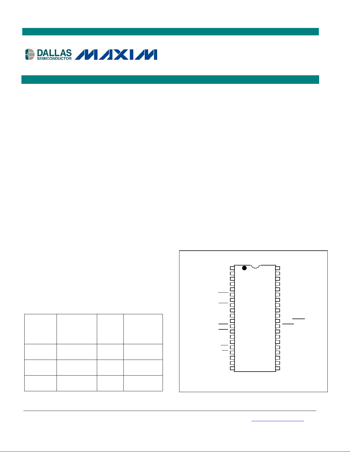
PIN CONFIGURATIONS
TOP VIEW
P1.0/T2
P1.1/T2EX
P1.2/RXD1
P1.3/TXD1
P1.4/INT2
P1.5/INT3
P1.6/INT4
P1.7/INT5
RST
P3.0/RXD0
P3.1/TXD0
P3.2/INT0
P3.3/INT1
P3.4/T0
P3.5/T1
P3.6/WR
P3.7/RD
XTAL2
XTAL1
VSS
Pin Configurations continued at end of data sheet.
1
2
3
4
5
6
7
8
9
DS89C420
10
11
12
13
14
15
16
17
18
19
20
DIP
40
39
38
37
36
35
34
33
32
31
30
29
28
27
26
25
24
23
22
21
VCC
P0.0
P0.1
P0.2
P0.3
P0.4
P0.5
P0.6
P0.7
EA/VPP
ALE/PROG
PSEN
P2.7
P2.6
P2.5
P2.4
P2.3
P2.2
P2.1
P2.0
Note: Some revisions of this device may incorporate deviations from published specifications known as errata. Multiple revisions of any device
may be simultaneously available through various sales channels. For information about device errata, click here: www.maxim-ic.com/errata.
1 of 59 103102

FEATURES
§ 80C52 compatible
- 8051 pin and instruction-set compatible
- Four bidirectional I/O ports
- Three 16-bit timer counters
- 256 bytes scratchpad RAM
§ On-chip memory
- 16kB flash memory
- In-system programmable through serial
port
- 1kB SRAM for MOVX
§ ROMSIZE feature
- Selects internal program memory size from
0 to 16k
- Allows access to entire external memory
map
- Dynamically adjustable by software
DS89C420
§ High-speed architecture
- 1 clock-per-machine cycle
- DC to 33MHz operation
- Single-cycle instruction in 30ns
- Optional variable length MOVX to access
fast/slow peripherals
- Dual data pointers with auto
increment/decrement and toggle select
- Supports four paged modes
§ Power Management Mode
- Programmable clock divider
- Automatic hardware and software exit
§ Two full-duplex serial ports
§ Programmable watchdog timer
§ 13 interrupt sources (six external)
§ Five levels of interrupt priority
§ Power-fail reset
§ Early warning power-fail interrupt
DETAILED DESCRIPTION
The DS89C420 is pin compatible with all three packages of the standard 8051 and includes standard
resources such as three timer/counters, four 8-bit I/O ports, and a serial port. It features 16kB of in-system
programmable flash memory, which can be programmed in-system from an I/O port using a built-in
program memory loader. It can also be loaded externally using standard commercially available
programmers.
Besides greater speed, the DS89C420 includes 1kB of data RAM, a second full-hardware serial port,
seven additional interrupts, two more levels of interrupt priority, programmable watchdog timer, brownout monitor, and power-fail reset. The device also provides dual data pointers (DPTRs) to speed up
block-data memory moves. This feature is further enhanced with a new selectable automatic
increment/decrement and toggle-select operation. The speed of MOVX data memory access can be
adjusted by adding stretch values up to 10 machine cycle times for flexibility in selecting external
memory and peripherals.
A power management mode (PMM) significantly consumes less power by slowing the CPU execution
rate from 1 clock period per cycle to 1024 clock periods per cycle. A selectable switchback feature can
automatically cancel this mode to enable a normal speed response to interrupts.
The EMI reduction feature disables the ALE signal when the processor is not accessing external memory.
2 of 59
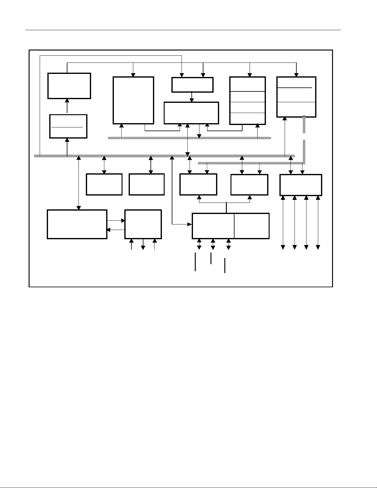
Figure 1. Block Diagram
DS89C420
Control &
Sequencer
Decoder
IR
Internal Control Bus
Serial I/O
Watchdog Timer
&
Power Manager
Internal
Registers
Timer /
Counters
Clock &
Reset
1
L
A
T
X
2
L
A
T
X
Interrupt
CPU
1Kx 8
RAM
Memory
Control
T
S
R
N
E
S
P
A
E
SFRs
DPTR
DPTR1
SP
16K x 8
Flash
ROM
Loader
G
O
R
P
/
E
L
PC
AR Inc
AR
Address Bus
I/O Ports
P0 P1
P2 P3
A
3 of 59

Table 1. Pin Description
DS89C420
PIN
DIP PLCC TQFP
40 12, 44 6, 38 V
20
1, 22, 23,3416, 17,
28, 39
NAME FUNCTION
CC
GND GND. Logic Ground
9 104RST
19
18
29 32 26
30 33 27
21
20
15
14
XTAL1
XTAL2
PSEN
ALE/
PROG
VCC - +5V
External Reset. The RST input pin is bidirectional and contains
a Schmitt trigger to recognize external active-high reset inputs.
The pin also employs an internal pulldown resistor to allow for a
combination of wire OR’d external reset sources. An RC is not
required for power-up, since the device provides this function
internally.
XTAL1, XTAL2. The crystal oscillator pins XTAL1 and
XTAL2 provide support for fundamental mode parallel resonant,
AT cut crystals. XTAL1 also acts as an input if there is an
external clock source in place of a crystal. XTAL2 serves as the
output of the crystal amplifier.
Program Store Enable. This signal is commonly connected to
optional external program memory as a chip enable.
PSEN
provides an active-low pulse and is driven high when external
program memory is not being accessed. In 1-cycle page mode 1,
PSEN remains low for consecutive page hits.
Address Latch Enable. Functions as a clock to latch the
external address LSB from the multiplexed address/data bus on
Port 0. This signal is commonly connected to the latch enable of
an external 373 family transparent latch. In default mode, ALE
has a pulse width of 1.5 XTAL1 cycles and a period of four
XTAL1 cycles. In page mode, the ALE pulse width is altered
according to the page mode selection. In traditional 8051 mode,
ALE is high when using the EMI reduction mode and during a
reset condition. ALE can be enabled by writing ALEON = 1
(PMR.2). Note that ALE operates independently of ALEON
during external memory accesses. As an alternate mode, this pin
(
PROG ) is used to execute the parallel program function.
39
38
37
36
35
34
33
32
43
42
41
40
39
38
37
36
37
36
35
34
33
32
31
30
P0.0 (AD0)
P0.1 (AD1)
P0.2 (AD2)
P0.3 (AD3)
P0.4 (AD4)
P0.5 (AD5)
P0.6 (AD6)
P0.7 (AD7)
Port 0 (AD0–7), I/O. Port 0 is an open-drain 8-bit, bidirectional
I/O port. As an alternate function, Port 0 can function as the
multiplexed address/data bus to access off-chip memory. During
the time when ALE is high, the LSB of a memory address is
presented. When ALE falls to a logic 0, the port transitions to a
bidirectional data bus. This bus is used to read external program
memory and read/write external RAM or peripherals. When
used as a memory bus, the port provides weak pullups for logic
1 outputs. The reset condition of Port 0 is three-state. Pullup
resistors are required when using Port 0 as an I/O port.
4 of 59

DS89C420
PIN
DIP PLCC TQFP
1–8 2–9 40–44
1
2
3
1
2
3
4
5
6
7
8
2
3
4
5
6
7
8
9
40
41
42
43
44
1
2
3
NAME FUNCTION
P1.0–P1.7
Port 1, I/O. Port 1 functions as both an 8-bit, bidirectional I/O
port and an alternate functional interface for timer 2 I/O, new
external interrupts, and new serial port 1. The reset condition of
port 1 is with all bits at a logic 1. In this state, a weak pullup
holds the port high. This condition also serves as an input state,
since any external circuit that writes to the port overcomes the
weak pullup. When software writes a 0 to any port pin, the
DS89C420 activates a strong pulldown that remains on until
either a 1 is written or a reset occurs. Writing a 1 after the port
has been at 0 causes a strong transition driver to turn on,
followed by a weaker sustaining pullup. Once the momentary
strong driver turns off, the port again becomes the output high
(and input) state. The alternate functions of Port 1 are outlined
below.
PORT ALTERNATE FUNCTION
P1.0 T2 External I/O for Timer/Counter2
P1.1 T2EX Timer 2 Capture/Reload Trigger
P1.2 RXD1 Serial Port 1 Receive
P1.3 TXD1 Serial Port 1 Transmit
P1.4 INT2 External Interrupt 2 (Positive Edge Detect)
P1.5
INT3 External Interrupt 3 (Negative Edge Detect)
P1.6 INT4 External Interrupt 4 (Positive Edge Detect)
P1.7
INT5 External Interrupt 5 (Negative Edge Detect)
21
22
23
24
25
26
27
28
24
25
26
27
28
29
30
31
18
19
20
21
22
23
24
25
P2.0 (A8)
P2.1 (A9)
P2.2 (A10)
P2.3 (A11)
P2.4 (A12)
P2.5 (A13)
P2.6 (A14)
P2.7 (A15)
Port 2 (A8–15), I/O. Port 2 is an 8-bit, bidirectional I/O port.
The reset condition of port 2 is logic high. In this state, a weak
pullup holds the port high. This condition also serves as an
input mode, since any external circuit that writes to the port
overcomes the weak pullup. When software writes a 0 to any
port pin, the DS89C420 activates a strong pulldown that
remains on until either a 1 is written or a reset occurs. Writing a
1 after the port has been at 0 causes a strong transition driver to
turn on, followed by a weaker sustaining pullup. Once the
momentary strong driver turns off, the port again becomes both
the output high and input state. As an alternate function, port 2
can function as the MSB of the external address bus when
reading external program memory and read/write external
RAM or peripherals. In page mode 1, port 2 provides both the
MSB and LSB of the external address bus; in page mode 2, it
provides the MSB and data.
5 of 59

DS89C420
PIN
DIP PLCC TQFP
NAME FUNCTION
10–17 11, 13–195, 7–13 P3.0–P3.7
10
11
12
13
14
15
16
17
31 35 29
11
13
14
15
16
17
18
19
5
7
8
9
10
11
12
13
P3.0
P3.1
P3.2
P3.3
P3.4
P3.5
P3.6
P3.7
EA
Port 3, I/O. Port 3 functions as both an 8-bit, bidirectional I/O
port and an alternate functional interface for external interrupts,
serial port 0, timer 0 and 1 inputs, and
RD
and WR strobes. The
reset condition of port 3 is with all bits at a logic 1. In this state,
a weak pullup holds the port high. This condition also serves as
an input mode, since any external circuit that writes to the port
overcomes the weak pullup. When software writes a 0 to any
port pin, the DS89C420 activates a strong pulldown that
remains on until either a 1 is written or a reset occurs. Writing a
1 after the port has been at 0 causes a strong transition driver to
turn on, followed by a weaker sustaining pullup. Once the
momentary strong driver turns off, the port again becomes both
the output high and input state. The alternate modes of Port 3
are outlined below.
PORT ALTERNATE FUNCTION
P3.0 RXD0 Serial Port 0 Receive
P3.1 TXD0 Serial Port 0 Transmit
P3.2
P3.3
INT0 External Interrupt 0
INT1 External Interrupt 1
P3.4 T0 Timer 0 External Input
P3.5 T1 Timer 1 External Input
P3.6
P3.7
WR External Data Memory Write Strobe
RD
External Data Memory Read Strobe
External Access. Allows selection of internal or external
program memory. Connect to ground to force the DS89C420 to
use an external memory-program memory. The internal RAM
is still accessible as determined by register settings. Connect to
to use internal flash memory.
V
CC
6 of 59

DS89C420
Compatibility
The DS89C420 is a fully static CMOS 8051-compatible microcontroller similar to the DS87C520 in
functional features, but with much higher performance. In most cases the DS89C420 can drop into an
existing socket for the 8xC51 family to improve the operation significantly. While remaining familiar to
8051 family users, it has many new features. The DS89C420 runs the standard 8051 family instruction set
and is pin compatible with DIP, PLCC, and TQFP packages. In general, software written for existing
8051-based systems works without DS89C420 modification, with the exception of critical timing
routines, since the DS89C420 performs its instructions much faster than the original for any given crystal
selection.
The DS89C420 provides three 16-bit timer/counters, two full-duplex serial ports, and 256 bytes of direct
RAM plus 1kB of extra MOVX RAM. I/O ports can operate as in standard 8051 products. Timers default
to a 12 clock-per-cycle operation to keep their timing compatible with original 8051 family systems.
However, timers are individually programmable to run at the new 1 clock-per-cycle if desired. The
DS89C420 provides several new hardware features implemented by new SFRs.
Performance Overview
The DS89C420 features a completely redesigned high-speed 8051-compatible core and allows operation
at a higher clock frequency, but the updated core does not have the dummy memory cycles that are
present in a standard 8051. A conventional 8051 generates machine cycles using the clock frequency
divided by 12. In the DS89C420, the same machine cycle takes 1 clock. Thus, the fastest instructions
execute 12 times faster for the same crystal frequency (and actually 24 times faster for the INC data
pointer instruction). It should be noted that this speed improvement reduces when using external memory
access modes that require more than 1 clock per cycle.
Improvement of individual programs depends on the actual instructions used. Speed-sensitive
applications make the most use of instructions that are 12 times faster. However, the sheer number of 12to-1 improved op codes makes dramatic speed improvements likely for any code. These architecture
improvements produce instruction cycle times as low as 30ns (33MIPs). The dual data pointer feature
also allows the user to eliminate wasted instructions when moving blocks of memory. The new page
modes allow for increased efficiency in external memory accesses.
Instruction Set Summary
All instructions perform the same functions as their 8051 counterparts. Their effect on bits, flags, and
other status functions is also identical. However, the timing of each instruction is different in both
absolute and relative number of clocks.
For absolute timing of real-time events, the timing of software loops can be calculated using information
in the “Instruction Set” table of the Ultra-High-Speed Flash Microcontroller User’s Guide. However,
counter/timers default to run at the older 12 clocks per increment. In this way, timer-based events occur at
the standard intervals with software executing at higher speed. Timers optionally can run at lower
numbers of clocks per increment to take advantage of faster processor operation.
The relative time of some instructions might be different in the new architecture than it was previously.
For example, in the original architecture, the “MOVX A, @DPTR” instruction and the “MOV direct,
direct” instruction used two machine cycles or 24 oscillator cycles. Therefore, they required the same
amount of time. In the DS89C420, the MOVX instruction takes as little as two machine cycles or two
oscillator cycles but the “MOV direct, direct” uses three machine cycles or three oscillator cycles. While
both are faster than their original counterparts, they now have different execution times. This is because
the DS89C420 usually uses one machine cycle for each instruction byte and requires one cycle for
7 of 59

DS89C420
execution. The user concerned with precise program timing should examine the timing of each instruction
to become familiar with the changes.
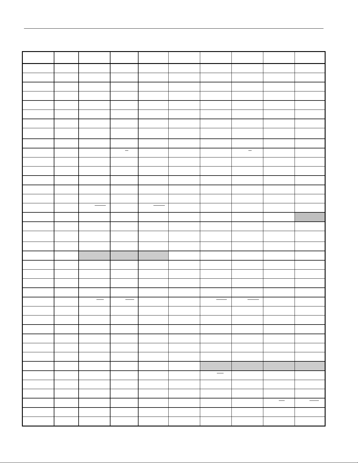
Special Function Registers (SFRs)
All peripherals and operations that are not explicit instructions in the DS89C420 are controlled through
SFRs. The most common features basic to the architecture are mapped to the SFRs. These include the
CPU registers (ACC, B, and PSW), data pointers (DPTRs), stack pointer, I/O ports, timer/counters, and
serial ports. In many cases, an SFR controls an individual function or reports the function’s status. The
SFRs reside in register locations 80h–FFh and are only accessible by direct addressing. SFRs whose
addresses end in 0h or 8h are bit-addressable.
All standard SFR locations from the 8051 are duplicated in the DS89C420 and several SFRs have been
added for the unique features of the DS89C420. Most of these features are controlled by bits in SFRs
located in unused locations in the 8051 SFR map. This allows for increased functionality while
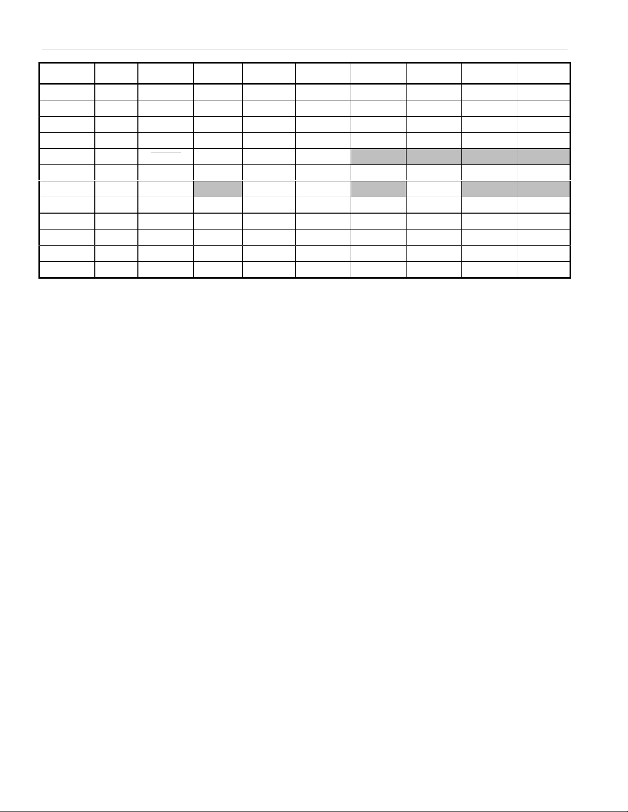
maintaining complete instruction set compatibility. Table 2 summarizes the SFRs and their locations.
Table 3 specifies the default reset condition for all SFR bits.
Data Pointers
The data pointers (DPTR and DPTR1) are used to assign a memory address for the MOVX instructions.
This address can point to a MOVX RAM location (on-chip or off-chip), or a memory-mapped peripheral.
Two pointers are useful when moving data from one memory area to another, or when using a memorymapped peripheral for both source and destination addresses. The user selects the active pointer through a
dedicated SFR bit (Sel = DPS.0), or activates an automatic toggling feature for altering the pointer
selection (TSL = DPS.5). An additional feature, if selected, provides automatic incrementing or
decrementing of the current DPTR.
Stack Pointer
The stack pointer denotes the register location at the top of the stack, which is the last used value. The
user can place the stack anywhere in the scratchpad RAM by setting the stack pointer to the desired
location, although the lower bytes are normally used for working registers.
I/O Ports
The DS89C420 offers four 8-bit I/O ports. Each I/O port is represented by an SFR location, and can be
written or read. The I/O port has a latch that contains the value written by software.
Counter/Timers
Three 16-bit timer/counters are available in the DS89C420. Each timer is contained in two SFR locations
that can be read or written by software. The timers are controlled by other SFRs described in the “SFR
Bit Description” section of the Ultra-High-Speed Flash Microcontroller User’s Guide.
Serial Ports
The DS89C420 provides two UARTs that are controlled and accessed by SFRs. Each UART has an
address that is used to read and write the UART. The same address is used for both read and write
operations, and the read and write operations are distinguished by the instruction. Each UART is
controlled by its own SFR control register.
8 of 59
DS89C420
Table 2. Special Function Registers
REGISTER ADDR BIT7 BIT6 BIT5 BIT4 BIT3 BIT2 BIT1 BIT0
P0 80h P0.7 P0.6 P0.5 P0.4 P0.3 P0.2 P0.1 P0.0
SP 81h —
DPL 82h
DPH 83h
DPL1 84h
DPH1 85h
DPS 86h ID1 ID0 TSL AID — — — SEL
PCON
TCON 88h TF1 TR1 TF0 TR0 IE1 IT1 IE0 IT0
TMOD 89h GATE C/ T M1 M0 GATE C/ T M1 M0
TL0 8Ah
TL1 8Bh
TH0 8Ch
TH1 8Dh
CKCON 8Eh WD1 WD0 T2M T1M T0M MD2 MD1 MD0
P1 90h P1.7/ 5INT P1.6/INT4 P1.5/ 3INT P1.4/INT2 P1.3/TXD1 P1.2/RXD1 P1.1/T2EX P1.0/T2
EXIF 91h IE5 IE4 IE3 IE2 CKRY RGMD RGSL BGS
CKMOD 96h
SCON0
SBUF0 99h
ACON 9Dh PAGEE PAGES1 PAGES0—————
P2 A0h P2.7 P2.6 P2.5 P2.4 P2.3 P2.2 P2.1 P2.0
IE A8h EA ES1 ET2 ES0 ET1 EX1 ET0 EX0
SADDR0 A9h
SADDR1 AAh
P3 B0h P3.7/ RD P3.6/ WR P3.5/T1 P3.4/T0 P3.3/ 1INT P3.2/ 0INT P3.1/TXD0 P3.0/RXD0
IP1 B1h — MPS1 MPT2 MPS0 MPT1 MPX1 MPT0 MPX0
IP0 B8h — LPS1 LPT2 LPS0 LPT1 LPX1 LPT0 LPX0
SADEN0 B9h
SADEN1 BAh
SCON1 C0h SM0/FE_1 SM1_1 SM2_1 REN_1 TB8_1 RB8_1 TI_1 RI_1
SBUF1 C1h —
ROMSIZE C2h —
PMR C4h CD1 CD0 SWB CTM 4X/ X2 ALEON DME1 DME0
STATUS C5h PIS2 PIS1 PIS0 — SPTA1 SPRA1 SPTA0 SPRA0
TA C7h —
T2CON C8h TF2 EXF2 RCLK TCLK EXEN2 TR2 C/ 2T CP/ 2RL
T2MOD C9h
RCAP2L CAh
87h SMOD_0 SMOD0 OFDF OFDE GF1 GF0 STOP IDLE
98h SM0/FE_0 SM1_0 SM2_0 REN_0 TB8_0 RB8_0 TI_0 RI_0
————————
————————
————————
————————
————————
————————
————————
————————
——
————————
————————
————————
————————
————————
——————
————————
———————
T2MH T1MH T0MH — — —
———————
—— —
———————
PRAME RMS2 RMS1 RMS0
T2OE DCEN
9 of 59
DS89C420
REGISTER ADDR BIT7 BIT6 BIT5 BIT4 BIT3 BIT2 BIT1 BIT0
RCAP2H CBh
TL2 CCh
TH2 CDh
PSW D0h CY AC F0 RS1 RS0 OV F1 P
FCNTL D5h FBUSY FERR
FDATA D6h
WDCON D8h SMOD_1 POR EPFI PFI WDIF WTRF EWT RWT
ACC E0h
EIE E8h — — — EWDI EX5 EX4 EX3 EX2
BF0h
EIP1 F1h — — — MPWDI MPX5 MPX4 MPX3 MPX2
EIP0 F8h — — — LPWDI LPX5 LPX4 LPX3 LPX2
————————
————————
————————
——
————————
————————
————————
FC3 FC2 FC1 FC0
10 of 59

DS89C420
Table 3. SFR Reset Value
REGISTER ADDR BIT7 BIT6 BIT5 BIT4 BIT3 BIT2 BIT1 BIT0
P0 80h1111111 1
SP 81h0000011 1
DPL 82h0000000 0
DPH 83h0000000 0
DPL1 84h0000000 0
DPH1 85h0000000 0
DPS 86h0000010 0
PCON 87h 0 0 Special Special 0 0 0 0
TCON 88h0000000 0
TMOD 89h0000000 0
TL0 8Ah0000000 0
TL1 8Bh0000000 0
TH0 8Ch0000000 0
TH1 8Dh0000000 0
CKCON 8Eh0000000 1
P1 90h1111111 1
EXIF 91h0000SpecialSpecialSpecial0
CKMOD 96h1100011 1
SCON0 98h0000000 0
SBUF0 99h0000000 0
ACON 9Dh0001111 1
P2 A0h1111111 1
IE A8h0000000 0
SADDR0 A9h0000000 0
SADDR1 AAh0000000 0
P3 B0h1111111 1
IP1 B1h1000000 0
IP0 B8h1000000 0
SADEN0 B9h0000000 0
SADEN1 BAh0000000 0
SCON1 C0h0000000 0
SBUF1 C1h0000000 0
ROMSIZE C2h1111010 1
PMR C4h1000000 0
STATUS C5h0001000 0
TA C7h1111111 1
T2CON C8h0000000 0
T2MOD C9h1111110 0
RCAP2L CAh0000000 0
RCAP2H CBh0000000 0
11 of 59

DS89C420
REGISTER ADDR BIT7 BIT6 BIT5 BIT4 BIT3 BIT2 BIT1 BIT0
TL2 CCh0000000 0
TH2 CDh0000000 0
PSW D0h0000000 0
FCNTL D5h1011000 0
FDATA D6h0000000 0
WDCON D8h 0 Special 0 Special 0 Special Special 0
ACC E0h0000000 0
EIE E8h1110000 0
B F0h0000000 0
EIP1 F1h1110000 0
EIP0 F8h1110000 0
12 of 59

DS89C420
Memory Organization
There are three distinct memory areas in the DS89C420: scratchpad registers, program memory, and data
memory. All registers are located on-chip but the program and data memory spaces can be either on-chip,
off-chip, or both. There are 16kB of on-chip program memory implemented in flash memory and 1kB of
on-chip data memory space that can be configured as program space using the PRAME bit in the
ROMSIZE feature. The DS89C420 uses a memory-addressing scheme that separates program memory
from data memory. The program and data segments can be overlapped since they are accessed in different
ways. If the maximum address of on-chip program or data memory is exceeded, the DS89C420 performs
an external memory access using the expanded memory bus. The PSEN signal goes active low to serve
as a chip enable or output enable when performing a code fetch from external program memory. MOVX
instructions activate the
bytes of on-chip flash memory store reset and interrupt vectors. The program memory ROMSIZE feature
allows software to dynamically configure the maximum address of on-chip program memory. This allows
the DS89C420 to act as a bootloader for an external flash or NV SRAM. It also enables the use of the
overlapping external program spaces.
256 bytes of on-chip RAM serve as a register area and program stack, which are separated from the data
memory.
RD or WR signal for external MOVX data memory access. The lower 128
Register Space
Registers are located in the 256 bytes of on-chip RAM, which can be divided into two subareas of 128
bytes each as illustrated in Figure 2. Separate classes of instructions are used to access the registers and
the program/data memory. The upper 128 bytes are overlapped with the 128 bytes of SFRs in the memory
map. The upper 128 bytes of scratchpad RAM are accessed by indirect addressing, and the SFR area is
accessed by direct addressing. The lower 128 bytes can be accessed by direct or indirect addressing.
There are four banks of eight individual working registers in the lower 128 bytes of scratchpad RAM.
The working registers are general-purpose RAM locations that can be addressed within the selected bank
by any instructions that use R0–R7. The register bank selection is controlled through the program status
register in the SFR area. The contents of the working registers can be used for indirectly addressing the
upper 128 bytes of scratchpad RAM.
To support the Boolean operations, there are individually addressable bits in both the RAM and SFR
areas. In the scratchpad RAM area, registers 20h–2Fh are bit-addressable by software using Boolean
operation instructions.
Another use of the scratchpad RAM area is for the stack. The stack pointer in the SFRs is used to select
storage locations for program variables and for return addresses of control operations.
13 of 59
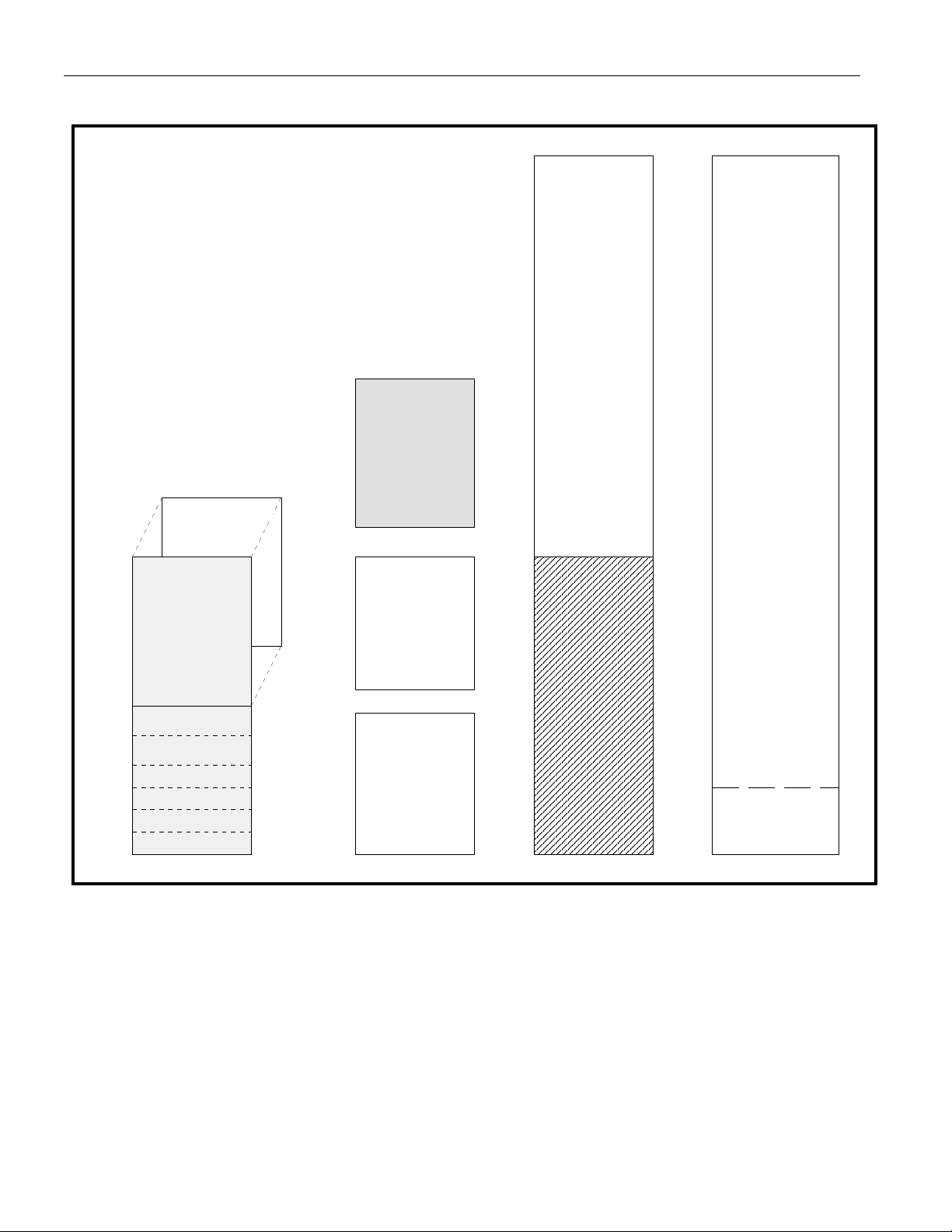
Figure 2. Memory Map
DS89C420
FF
128 Bytes
Indirect
Addressing
80
7F
2F
Bit Addressable
20
1F
00
INTERNAL
REGISTERS
128 Bytes SFR
Bank 3
Bank 2
Bank 1
Bank 0
03FF
0000
3FFF
2000
1FFF
0000
INTERNAL
MEMORY
1K x 8
SRAM
Data OR
prog mem
addr from
400 - 7FF
8K x 8
Flash
Memory
(Program)
8K x 8
Flash
Memory
(Program)
FFFF
4000
External
Program
Memory
FFFF
External
Data
Memory
03FF
00000000
14 of 59

DS89C420
Memory Configuration
As illustrated in Figure 2, the DS89C420 incorporates two 8kB flash memories for on-chip program
memory and 1kB of SRAM for on-chip data memory or a particular range (400–7FF) of “alternate”
program memory space. The DS89C420 uses an address scheme that separates program memory from
data memory, such that the 16-bit address bus can address each memory area up to 64kB.
Program Memory Access
On-chip program memory begins at address 0000h and is contiguous through 3FFFh (16kB). Exceeding
the maximum address of on-chip program memory causes the device to access off-chip memory.
However, the maximum on-chip decoded address is selectable by software using the ROMSIZE feature.
Software can cause the DS89C420 to behave like a device with less on-chip memory. This is beneficial
when overlapping external memory is used. The maximum memory size is dynamically variable. Thus, a
portion of memory can be removed from the memory map to access off-chip memory, then be restored to
access on-chip memory. In fact, all of the on-chip memory can be removed from the memory map
allowing the full 64kB memory space to be addressed from off-chip memory. Program memory addresses
that are larger than the selected maximum are automatically fetched from outside the part through ports 0
and 2 (Figure 2).
The ROMSIZE register is used to select the maximum on-chip decoded address for program memory.
Bits RMS2, RMS1, RMS0 have the following effect:
RMS2 RMS1
00 00k
0 0 1 1k/03FFh
0 1 0 2k/07FFh
0 1 1 4k/0FFFh
1 0 0 8k/1FFFh
1 0 1 16k (default)/3FFFh
1 1 0 Invalid–Reserved
1 1 1 Invalid–Reserved
RMS0
ADDRESS
MAXIMUM ON-CHIP
PROGRAM MEMORY
The reset default condition is a maximum on-chip program-memory address of 16kB. When accessing
external program memory, the first 16kB would be inaccessible. To select a smaller effective program
memory size, software must alter bits RMS2–RMS0. Altering these bits requires a timed access
procedure as explained later.
Care should be taken so that changing the ROMSIZE register does not corrupt program execution. For
example, assume that a DS89C420 is executing instructions from internal program memory near the
12kB boundary (~3000h) and that the ROMSIZE register is currently configured for a 16kB internal
program space. If software reconfigures the ROMSIZE register to 4kB (0000h–0FFFh) in the current
state, the device immediately jumps to external program execution because program code from 4kB to
16kB (1000h–3FFFh) is no longer located on-chip. This could result in code misalignment and execution
of an invalid instruction. The recommended method is to modify the ROMSIZE register from a location
in memory that is internal (or external) both before and after the operation. In the above example, the
instruction that modifies the ROMSIZE register should be located below the 4kB (1000h) boundary or
above the 16kB (3FFFh) boundary so that it is unaffected by the memory modification. The same
precaution should be applied if the internal program memory size is modified while executing from
external program memory.
15 of 59

DS89C420
For non-page mode operations, off-chip memory is accessed using the multiplexed address/data bus on
P0 and the MSB address on P2. While serving as a memory bus, these pins are not I/O ports. This
convention follows the standard 8051 method of expanding on-chip memory. Off-chip program memory
access also occurs if the
EA pin is a logic 0. EA overrides all bit settings. The PSEN signal goes active
(low) to serve as a chip enable or output enable when port 0 and port 2 fetch from external program
memory.
RD and WR signals are used to control the external data memory device. Data memory is accessed
The
by MOVX instructions. The MOVX@Ri instruction uses the value in the designated working register to
provide the LSB of the address, while port 2 supplies the address MSB. The MOVX@DPTR instruction
uses one of the two data pointers to move data over the entire 64kB external data memory space.
Software selects the data pointer to be used by writing to the SEL bit (DPS.0).
The DS89C420 also provides a user option for high-speed external memory access by reconfiguring the
external memory interface into page mode operation.
Note: When using the original 8051 expanded bus structure, the throughput is reduced by 75% compared
with that of internal operations. This is due to the CPU being stalled for three out of four clocks waiting
for the data fetch, which takes four clocks. Page Mode 1 is the only external addressing mode where the
CPU does not require stalls for external memory access, but page misses result in reduced external access
performance.
On-Chip Program Memory
The full on-chip program memory range can be fetched by the processor automatically. The reset routines
and all interrupt vectors are located in the lower 128 bytes of the on-chip program memory area.
On-chip program memory is logically divided into two 8kB flash memory banks and is designed to be
programmed with the standard 5V V
supply by using a built-in program memory loader. It can also be
CC
programmed in standard flash or EPROM programmers. The DS89C420 incorporates a memory
management unit (MMU) and other hardware to support any of the two programming methods. The
MMU controls program and data memory access, and provides sequencing and timing controls for
programming the on-chip program memory. There is also a separate security flash block that is used to
support a standard three-level lock, a 64-byte encryption array, and other flash options.
Security Features
The DS89C420 incorporates a 64-byte encryption array, allowing the user to verify program codes while
viewing the data in encrypted form. The encryption array is implemented in a security flash memory
block that has the same electrical and timing characteristics as the on-chip program memory. Once the
encryption array is programmed to non-FFh, the data presented in the verify mode is encrypted. Each
byte of data is XNOR’ed with a byte in the encryption array during verification.
A three-level lock restricts viewing of the internal program and data memory contents. By programming
the three lock bits, the user can select a level of security as specified in Table 4. Once a security level is
selected and programmed, the setting of the lock bits remains. Only a mass erase can erase these bits to
allow reprogramming the security level to a less restricted protection.
16 of 59

Table 4. Flash Memory Lock Bits
LEVEL LB1 LB2 LB3 PROTECTION
DS89C420
1111
2011
3X01
4 X X 0 Level 3 plus no external execution.
No program lock. Encrypted verify if encryption array is
programmed.
Prevent MOVC in external memory from reading program code in
internal memory. EA is sampled and latched on reset. Allow no
further parallel or program memory loader programming.
Level 2 plus no verify operation. Also prevent MOVX in external
memory from reading internal SRAM.
The DS89C420 provides user-selectable options that must be set before beginning software execution.
The option control register uses flash bits rather than SFRs, and is individually erasable and
programmable as a byte-wide register. Bit 3 of this register is defined as the watchdog POR default.
Setting this bit to 1 disables the watchdog reset function on power-up, and clearing this bit to 0 enables
the watchdog reset function automatically. Other bits of this register are undefined and are at logic 1
when read. The value of this register can be read at address FCh in parallel programming mode or when
executing a verify-option control-register instruction in ROM loader mode.
The signature bytes can be read in ROM loader mode or in parallel programming mode. Reading data
from addresses 30h, 31h, and 60h provides signature information about manufacturer, part, and extension
as follows:
ADDRESS VALUE FUNCTION
30h DAh Manufacturer ID
31h 42h DS89C420 Device ID
60h 01h Device Extension
ROM Loader
The full 16kB of on-chip flash program-memory space, security flash block, and external SRAM can be
programmed in-system from an external source through serial port 0 under the control of a built-in ROM
loader. The ROM loader also has an auto-baud feature that determines which baud rate frequencies are
being used for communication and sets up the baud rate generator for communication at that frequency.
When the DS89C420 is powered up and has entered its user operating mode, the ROM loader mode can
be invoked at any time by forcing RST = 1,
down or when the condition (RST = 1 and
forces the processor to start fetching from the 2kB internal ROM for program memory initialization and
other loader functions.
The read/write accessibility is determined by the state of the lock bits, which can be verified directly by
the ROM loader. In the ROM loader mode, a mass-erase operation also erases the memory bank select
and sets it to the default state. Otherwise, the memory bank select cannot be altered in the ROM loader
mode.
EA = 0, and PSEN = 0. It remains in effect until power-
PSEN = EA = 0) is removed. Entering the ROM loader mode
17 of 59
DS89C420
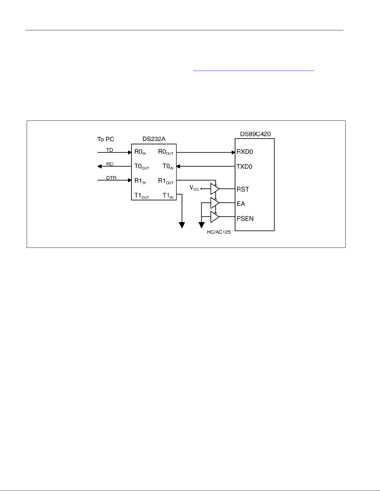
Flash programming is executed by a series of internal flash commands that are derived (by the built-in
ROM loader) from data transmitted over the serial interface from a host PC. PC-based software tools that
configure and load the microcontrollers are available at www.maxim-ic.com/micros/ftpinfo.html.
Full details of the ROM loader software and its implementation are given in the Ultra-High-Speed Flash
Microcontroller User’s Guide.
Figure 3. Interfacing the Bootloader to a PC
18 of 59
