


DS80CH11
System Energy Manager
DS80CH11
011200 1/88
PRODUCT SPECIFICATION
V2.1

DS80CH11
011200 2/88
1.0 GENERAL DESCRIPTION 5. . . . . . . . . . . . . . . . . . . . . . . . . . . . . . . . . . . . . . . . . . . . . . . . . . . . . . . . . . . . . . . . . .
1.1 OVERVIEW 5. . . . . . . . . . . . . . . . . . . . . . . . . . . . . . . . . . . . . . . . . . . . . . . . . . . . . . . . . . . . . . . . . . . . . . . .
1.2 DETAILED FEATURE SUMMARY 7. . . . . . . . . . . . . . . . . . . . . . . . . . . . . . . . . . . . . . . . . . . . . . . . . . . . .
1.3 CONVENTIONS 7. . . . . . . . . . . . . . . . . . . . . . . . . . . . . . . . . . . . . . . . . . . . . . . . . . . . . . . . . . . . . . . . . . . .
1.4 ADDITIONAL REFERENCES 7. . . . . . . . . . . . . . . . . . . . . . . . . . . . . . . . . . . . . . . . . . . . . . . . . . . . . . . . .
2.0 PIN DESCRIPTION 8. . . . . . . . . . . . . . . . . . . . . . . . . . . . . . . . . . . . . . . . . . . . . . . . . . . . . . . . . . . . . . . . . . . . . . . .
2.1 PIN FUNCTION SUMMARY 9. . . . . . . . . . . . . . . . . . . . . . . . . . . . . . . . . . . . . . . . . . . . . . . . . . . . . . . . . .
2.2 PIN CHARACTERISTICS 14. . . . . . . . . . . . . . . . . . . . . . . . . . . . . . . . . . . . . . . . . . . . . . . . . . . . . . . . . . .
3.0 CORE MICROCONTROLLER 19. . . . . . . . . . . . . . . . . . . . . . . . . . . . . . . . . . . . . . . . . . . . . . . . . . . . . . . . . . . . . .
3.1 CORE MICRO OVERVIEW 19. . . . . . . . . . . . . . . . . . . . . . . . . . . . . . . . . . . . . . . . . . . . . . . . . . . . . . . . . .
3.2 INSTRUCTION SET SUMMARY 19. . . . . . . . . . . . . . . . . . . . . . . . . . . . . . . . . . . . . . . . . . . . . . . . . . . . .
3.3 SPEED IMPROVEMENT 21. . . . . . . . . . . . . . . . . . . . . . . . . . . . . . . . . . . . . . . . . . . . . . . . . . . . . . . . . . . .
3.4 INSTRUCTION SET ADDITIONAL REFERENCES 21. . . . . . . . . . . . . . . . . . . . . . . . . . . . . . . . . . . . .
3.5 RESET 21. . . . . . . . . . . . . . . . . . . . . . . . . . . . . . . . . . . . . . . . . . . . . . . . . . . . . . . . . . . . . . . . . . . . . . . . . . .
3.6 INTERRUPT CONTROL 22. . . . . . . . . . . . . . . . . . . . . . . . . . . . . . . . . . . . . . . . . . . . . . . . . . . . . . . . . . . .
4.0 MEMORY RESOURCES 24. . . . . . . . . . . . . . . . . . . . . . . . . . . . . . . . . . . . . . . . . . . . . . . . . . . . . . . . . . . . . . . . . . .
4.1 OVERVIEW 24. . . . . . . . . . . . . . . . . . . . . . . . . . . . . . . . . . . . . . . . . . . . . . . . . . . . . . . . . . . . . . . . . . . . . . .
4.2 DATA MEMORY ACCESS 24. . . . . . . . . . . . . . . . . . . . . . . . . . . . . . . . . . . . . . . . . . . . . . . . . . . . . . . . . . .
4.2.1 Stretch Memory Cycle 24. . . . . . . . . . . . . . . . . . . . . . . . . . . . . . . . . . . . . . . . . . . . . . . . . . . . . .
4.2.2 Dual Data Pointer 25. . . . . . . . . . . . . . . . . . . . . . . . . . . . . . . . . . . . . . . . . . . . . . . . . . . . . . . . . .
4.3 EXTERNAL MEMORY INTERFACE 25. . . . . . . . . . . . . . . . . . . . . . . . . . . . . . . . . . . . . . . . . . . . . . . . . .
4.4 DIRECT (SCRATCHPAD) RAM ACCESS 25. . . . . . . . . . . . . . . . . . . . . . . . . . . . . . . . . . . . . . . . . . . . .
4.5 SPECIAL FUNCTION REGISTERS 25. . . . . . . . . . . . . . . . . . . . . . . . . . . . . . . . . . . . . . . . . . . . . . . . . .
5.0 CORE I/O RESOURCES 30. . . . . . . . . . . . . . . . . . . . . . . . . . . . . . . . . . . . . . . . . . . . . . . . . . . . . . . . . . . . . . . . . . .
5.1 PROGRAMMABLE TIMERS 30. . . . . . . . . . . . . . . . . . . . . . . . . . . . . . . . . . . . . . . . . . . . . . . . . . . . . . . . .
5.2 SERIAL PORTS 30. . . . . . . . . . . . . . . . . . . . . . . . . . . . . . . . . . . . . . . . . . . . . . . . . . . . . . . . . . . . . . . . . . .
5.3 WATCHDOG TIMER 30. . . . . . . . . . . . . . . . . . . . . . . . . . . . . . . . . . . . . . . . . . . . . . . . . . . . . . . . . . . . . . .
5.4 PARALLEL I/O PORTS 31. . . . . . . . . . . . . . . . . . . . . . . . . . . . . . . . . . . . . . . . . . . . . . . . . . . . . . . . . . . . .
5.4.1 Alternate Pin Function Summary 31. . . . . . . . . . . . . . . . . . . . . . . . . . . . . . . . . . . . . . . . . . . . .
6.0 2–Wire SERIAL INTERFACE 33. . . . . . . . . . . . . . . . . . . . . . . . . . . . . . . . . . . . . . . . . . . . . . . . . . . . . . . . . . . . . . .
6.1 INTRODUCTION 33. . . . . . . . . . . . . . . . . . . . . . . . . . . . . . . . . . . . . . . . . . . . . . . . . . . . . . . . . . . . . . . . . .
6.2 REGISTER DESCRIPTION 34. . . . . . . . . . . . . . . . . . . . . . . . . . . . . . . . . . . . . . . . . . . . . . . . . . . . . . . . .
6.2.1 2WFSx – 2–Wire Frequency Select Registers 34. . . . . . . . . . . . . . . . . . . . . . . . . . . . . . . . . .
6.2.2 2WDATx – 2–Wire Data I/O Registers 34. . . . . . . . . . . . . . . . . . . . . . . . . . . . . . . . . . . . . . . .
6.2.3 2WSADRx – 2–Wire Slave Address Registers 34. . . . . . . . . . . . . . . . . . . . . . . . . . . . . . . . .
6.2.4 2WCONx – 2–Wire Control Registers 35. . . . . . . . . . . . . . . . . . . . . . . . . . . . . . . . . . . . . . . . .
6.2.5 2WSTAT1x – 2–Wire Status Register 1 36. . . . . . . . . . . . . . . . . . . . . . . . . . . . . . . . . . . . . . . .
6.2.6 2WSTAT2x – 2–Wire Status Register 2 36. . . . . . . . . . . . . . . . . . . . . . . . . . . . . . . . . . . . . . . .
6.3 OPERATION DESCRIPTION 37. . . . . . . . . . . . . . . . . . . . . . . . . . . . . . . . . . . . . . . . . . . . . . . . . . . . . . . .
6.3.1 Master Transmit 38. . . . . . . . . . . . . . . . . . . . . . . . . . . . . . . . . . . . . . . . . . . . . . . . . . . . . . . . . . .
6.3.2 Master Receive 39. . . . . . . . . . . . . . . . . . . . . . . . . . . . . . . . . . . . . . . . . . . . . . . . . . . . . . . . . . . .
6.3.3 Slave Receive 40. . . . . . . . . . . . . . . . . . . . . . . . . . . . . . . . . . . . . . . . . . . . . . . . . . . . . . . . . . . . .
TABLE OF CONTENTS

DS80CH11
011200 3/88
6.3.4 Slave Transmit 41. . . . . . . . . . . . . . . . . . . . . . . . . . . . . . . . . . . . . . . . . . . . . . . . . . . . . . . . . . . .
6.3.5 Bus Monitor Mode Operation 43. . . . . . . . . . . . . . . . . . . . . . . . . . . . . . . . . . . . . . . . . . . . . . . .
7.0 A/D CONVERTER 44. . . . . . . . . . . . . . . . . . . . . . . . . . . . . . . . . . . . . . . . . . . . . . . . . . . . . . . . . . . . . . . . . . . . . . . .
7.1 OVERVIEW 44. . . . . . . . . . . . . . . . . . . . . . . . . . . . . . . . . . . . . . . . . . . . . . . . . . . . . . . . . . . . . . . . . . . . . . .
7.2 ANALOG POWER / SLEEP MODE 44. . . . . . . . . . . . . . . . . . . . . . . . . . . . . . . . . . . . . . . . . . . . . . . . . . .
7.3 REFERENCE OPTION 45. . . . . . . . . . . . . . . . . . . . . . . . . . . . . . . . . . . . . . . . . . . . . . . . . . . . . . . . . . . . .
7.4 SAR A/D CONVERTER 45. . . . . . . . . . . . . . . . . . . . . . . . . . . . . . . . . . . . . . . . . . . . . . . . . . . . . . . . . . . . .
7.5 CONVERSION TIME 46. . . . . . . . . . . . . . . . . . . . . . . . . . . . . . . . . . . . . . . . . . . . . . . . . . . . . . . . . . . . . . .
7.6 WINDOW COMPARATOR 47. . . . . . . . . . . . . . . . . . . . . . . . . . . . . . . . . . . . . . . . . . . . . . . . . . . . . . . . . .
7.7 A/D OPERATION 48. . . . . . . . . . . . . . . . . . . . . . . . . . . . . . . . . . . . . . . . . . . . . . . . . . . . . . . . . . . . . . . . . .
7.8 A/D SPECIAL FUNCTION REGISTERS 49. . . . . . . . . . . . . . . . . . . . . . . . . . . . . . . . . . . . . . . . . . . . . . .
7.8.1 ADCON1 – A/D Control Register 1 49. . . . . . . . . . . . . . . . . . . . . . . . . . . . . . . . . . . . . . . . . . .
7.8.2 ADCON2 – A/D Control Register 2 50. . . . . . . . . . . . . . . . . . . . . . . . . . . . . . . . . . . . . . . . . . .
7.8.3 ADMSB – A/D Result Most Significant Byte 50. . . . . . . . . . . . . . . . . . . . . . . . . . . . . . . . . . . .
7.8.4 ADLSB – A/D Result Least Significant Byte 51. . . . . . . . . . . . . . . . . . . . . . . . . . . . . . . . . . . .
7.8.5 WINHI – A/D Window Comparator High Byte 51. . . . . . . . . . . . . . . . . . . . . . . . . . . . . . . . . . .
7.8.6 WINLO – A/D Window Comparator Low Byte 51. . . . . . . . . . . . . . . . . . . . . . . . . . . . . . . . . .
8.0 ACTIVITY MONITOR/LED CONTROL 52. . . . . . . . . . . . . . . . . . . . . . . . . . . . . . . . . . . . . . . . . . . . . . . . . . . . . . .
8.1 OVERVIEW 52. . . . . . . . . . . . . . . . . . . . . . . . . . . . . . . . . . . . . . . . . . . . . . . . . . . . . . . . . . . . . . . . . . . . . . .
8.2 ACTIVITY MONITOR INPUT OPERA TION 52. . . . . . . . . . . . . . . . . . . . . . . . . . . . . . . . . . . . . . . . . . . .
8.3 AME – ACTIVITY MONITOR ENABLE REGISTER 53. . . . . . . . . . . . . . . . . . . . . . . . . . . . . . . . . . . . .
8.4 AMQ – ACTIVITY MONITOR QUALIFIER REGISTER 53. . . . . . . . . . . . . . . . . . . . . . . . . . . . . . . . . .
8.5 AMP – ACTIVITY MONITOR POLARITY REGISTER 54. . . . . . . . . . . . . . . . . . . . . . . . . . . . . . . . . . .
8.6 AMF – ACTIVITY MONITOR FLAG REGISTER 54. . . . . . . . . . . . . . . . . . . . . . . . . . . . . . . . . . . . . . . .
8.7 LED CONTROL 54. . . . . . . . . . . . . . . . . . . . . . . . . . . . . . . . . . . . . . . . . . . . . . . . . . . . . . . . . . . . . . . . . . . .
9.0 HOST INTERFACE PORTS 55. . . . . . . . . . . . . . . . . . . . . . . . . . . . . . . . . . . . . . . . . . . . . . . . . . . . . . . . . . . . . . . .
9.1 OVERVIEW 55. . . . . . . . . . . . . . . . . . . . . . . . . . . . . . . . . . . . . . . . . . . . . . . . . . . . . . . . . . . . . . . . . . . . . . .
9.2 REGISTER MAPPING 55. . . . . . . . . . . . . . . . . . . . . . . . . . . . . . . . . . . . . . . . . . . . . . . . . . . . . . . . . . . . . .
9.3 KBDIN / PMDIN – DATA REGISTERS 56. . . . . . . . . . . . . . . . . . . . . . . . . . . . . . . . . . . . . . . . . . . . . . . .
9.4 KBSTAT / PMSTAT – STATUS REGISTERS 57. . . . . . . . . . . . . . . . . . . . . . . . . . . . . . . . . . . . . . . . . . .
9.5 KBDOUT / PMDOUT – OUTPUT DATA REGISTERS 58. . . . . . . . . . . . . . . . . . . . . . . . . . . . . . . . . . .
10.0 KEYBOARD SCANNING PORTS 59. . . . . . . . . . . . . . . . . . . . . . . . . . . . . . . . . . . . . . . . . . . . . . . . . . . . . . . . . . .
10.1 OVERVIEW 59. . . . . . . . . . . . . . . . . . . . . . . . . . . . . . . . . . . . . . . . . . . . . . . . . . . . . . . . . . . . . . . . . . . . . . .
10.2 KEY SCAN OUTPUTS 59. . . . . . . . . . . . . . . . . . . . . . . . . . . . . . . . . . . . . . . . . . . . . . . . . . . . . . . . . . . . . .
10.3 KEY SCAN INPUTS 59. . . . . . . . . . . . . . . . . . . . . . . . . . . . . . . . . . . . . . . . . . . . . . . . . . . . . . . . . . . . . . . .
10.4 KDE – KEY DETECT ENABLE REGISTER 59. . . . . . . . . . . . . . . . . . . . . . . . . . . . . . . . . . . . . . . . . . . .
10.5 KDF – KEYBOARD DETECT FLAG REGISTER 59. . . . . . . . . . . . . . . . . . . . . . . . . . . . . . . . . . . . . . . .
11.0 PULSE WIDTH MODULAT ORS 60. . . . . . . . . . . . . . . . . . . . . . . . . . . . . . . . . . . . . . . . . . . . . . . . . . . . . . . . . . . . .
11.1 FUNCTION OVERVIEW 60. . . . . . . . . . . . . . . . . . . . . . . . . . . . . . . . . . . . . . . . . . . . . . . . . . . . . . . . . . . .
11.2 PRESCALER 60. . . . . . . . . . . . . . . . . . . . . . . . . . . . . . . . . . . . . . . . . . . . . . . . . . . . . . . . . . . . . . . . . . . . . .
11.3 PWM CLOCK GENERATORS 60. . . . . . . . . . . . . . . . . . . . . . . . . . . . . . . . . . . . . . . . . . . . . . . . . . . . . . .
11.4 PWM PULSE GENERAT ORS 61. . . . . . . . . . . . . . . . . . . . . . . . . . . . . . . . . . . . . . . . . . . . . . . . . . . . . . .
11.5 PWM SPECIAL FUNCTION REGISTERS 62. . . . . . . . . . . . . . . . . . . . . . . . . . . . . . . . . . . . . . . . . . . . .
11.5.1 PW01CS / PW23CS – PWM 0, 1 / PWM 2, 3 Clock Select Registers 62. . . . . . . . . . . . . .
11.5.2 PW01CON / PW23CON – PWM 0, 1 / PWM 2, 3 Control Register 63. . . . . . . . . . . . . . . .
11.5.3 PWnFG – PWM n Frequency Generator Registers 63. . . . . . . . . . . . . . . . . . . . . . . . . . . . . .
11.5.4 PWMn – PWM n Value Registers 64. . . . . . . . . . . . . . . . . . . . . . . . . . . . . . . . . . . . . . . . . . . . .
12.0 MICROCONTROLLER POWER MANAGEMENT 66. . . . . . . . . . . . . . . . . . . . . . . . . . . . . . . . . . . . . . . . . . . . .
12.1 POWER–DOWN / POWER–UP OPERATION 66. . . . . . . . . . . . . . . . . . . . . . . . . . . . . . . . . . . . . . . . . .

DS80CH11
011200 4/88
12.1.1 Microcontroller Power Fail Reset 66. . . . . . . . . . . . . . . . . . . . . . . . . . . . . . . . . . . . . . . . . . . . .
12.2 LOW POWER OPERATING MODES 66. . . . . . . . . . . . . . . . . . . . . . . . . . . . . . . . . . . . . . . . . . . . . . . . .
12.2.1 Slow Clock Mode 66. . . . . . . . . . . . . . . . . . . . . . . . . . . . . . . . . . . . . . . . . . . . . . . . . . . . . . . . . .
12.2.1.1 Crystaless Slow Clock Mode 67. . . . . . . . . . . . . . . . . . . . . . . . . . . . . . . . . . . . . . . . . . . . . . . .
12.2.1.2 Slow Clock Mode Operation 67. . . . . . . . . . . . . . . . . . . . . . . . . . . . . . . . . . . . . . . . . . . . . . . . .
12.2.1.3 Clock Divider 67. . . . . . . . . . . . . . . . . . . . . . . . . . . . . . . . . . . . . . . . . . . . . . . . . . . . . . . . . . . . . .
12.2.1.4 Switchback 68. . . . . . . . . . . . . . . . . . . . . . . . . . . . . . . . . . . . . . . . . . . . . . . . . . . . . . . . . . . . . . . .
12.2.1.5 Status 68. . . . . . . . . . . . . . . . . . . . . . . . . . . . . . . . . . . . . . . . . . . . . . . . . . . . . . . . . . . . . . . . . . . .
12.2.1.6 Crystal / Ring Operation 68. . . . . . . . . . . . . . . . . . . . . . . . . . . . . . . . . . . . . . . . . . . . . . . . . . . .
12.2.2 Idle Mode 71. . . . . . . . . . . . . . . . . . . . . . . . . . . . . . . . . . . . . . . . . . . . . . . . . . . . . . . . . . . . . . . . .
12.2.3 Stop Mode and Enhancements 71. . . . . . . . . . . . . . . . . . . . . . . . . . . . . . . . . . . . . . . . . . . . . .
13.0 +5.0V ELECTRICAL SPECIFICATIONS 74. . . . . . . . . . . . . . . . . . . . . . . . . . . . . . . . . . . . . . . . . . . . . . . . . . . . .
13.1 ABSOLUTE MAXIMUM RATINGS* 74. . . . . . . . . . . . . . . . . . . . . . . . . . . . . . . . . . . . . . . . . . . . . . . . . . .
13.2 MICROCONTROLLER DC ELECTRICAL CHARACTERISTICS 74. . . . . . . . . . . . . . . . . . . . . . . . . .
13.3 MICROCONTROLLER AC ELECTRICAL CHARACTERISTICS 76. . . . . . . . . . . . . . . . . . . . . . . . . .
13.3.1 External Program Memory Characteristics 76. . . . . . . . . . . . . . . . . . . . . . . . . . . . . . . . . . . . .
13.3.2 MOVX Using Stretch Memory Cycles 77. . . . . . . . . . . . . . . . . . . . . . . . . . . . . . . . . . . . . . . . .
13.3.3 External Clock Characteristics 78. . . . . . . . . . . . . . . . . . . . . . . . . . . . . . . . . . . . . . . . . . . . . . .
13.3.4 Serial Port Mode 0 Timing Characteristics 78. . . . . . . . . . . . . . . . . . . . . . . . . . . . . . . . . . . . .
13.3.5 Power Cycle Timing Characteristics 79. . . . . . . . . . . . . . . . . . . . . . . . . . . . . . . . . . . . . . . . . .
13.4 SYSTEM INTERFACE DC ELECTRICAL CHARACTERISTICS 83. . . . . . . . . . . . . . . . . . . . . . . . . .
13.5 HOST I/F AC TIMING CHARACTERISTICS 84. . . . . . . . . . . . . . . . . . . . . . . . . . . . . . . . . . . . . . . . . . .
13.6 2–Wire AC TIMING CHARACTERISTICS 86. . . . . . . . . . . . . . . . . . . . . . . . . . . . . . . . . . . . . . . . . . . . .
13.7 A/D CONVERTER SPECIFICATIONS 87. . . . . . . . . . . . . . . . . . . . . . . . . . . . . . . . . . . . . . . . . . . . . . . .
13.7.1 Absolute Maximum Ratings 87. . . . . . . . . . . . . . . . . . . . . . . . . . . . . . . . . . . . . . . . . . . . . . . . . .
13.7.2 A/D Electrical Characteristics 87. . . . . . . . . . . . . . . . . . . . . . . . . . . . . . . . . . . . . . . . . . . . . . . .

DS80CH11
011200 5/88
1.0 GENERAL DESCRIPTION
1.1 OVERVIEW
The System Energy Manager is a highly integrated
microcontroller that provides several key features for
systems including key scanning and control, battery
and power management, as well as two 2–Wire serial
I/O Ports. It incorporates the Dallas 8051–compatible
high–speed microcontroller core which has been redesigned to eliminate wasted clock and memory cycles.
Every standard 8051 instruction is executed between
1.5 and 3 times faster than the original for the same
crystal speed. Looking at it another way, the high–
speed core achieves the same throughput as a standard 8051 while using much less power as a result of
fewer required clock cycles. As a result, the firmware
can easily support many tasks required by mobile systems within a single component.
The controller is designed to off–load battery and power
management tasks from the host CPU and thereby
make possible an efficient solution for systems. In addition to the microcontroller core, it incorporates an
8–channel, 10–bit A/D converter with external reference so that its firmware can perform battery management tasks without burdening the host CPU. A four–
channel 8–bit pulse–width modulator allows digital
control of functions such as LCD contrast and brightness. An 8–bit port is provided for key scan inputs. A
total of 88 parallel I/O pins are available for key scanning, system configuration, and power management
control.
The System Energy Manager scans a key matrix and
interfaces to the host CPU via an 8042–compatible port.
The benefits of sophisticated power management and
permanently powered functions are thereby attained
without adding to the system’s chip count.
Two 2–wire, bi–directional serial buses are incorporated to facilitate the management of slave peripheral
devices on the motherboard, such as digital temperature sensors and potentiometers, and to support external low–speed I/O devices such as monitor configuration channels, pen tablets, and joysticks.
Because a direct interface to the X–bus is provided, the
controller is not dependent on a particular core logic
chip or chip set. Independent chip select inputs for the
keyboard controller, power management #1, and power
management #2 registers are provided.
DS80CH11
011200 6/88
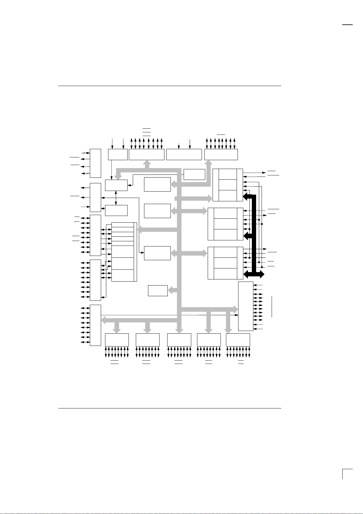
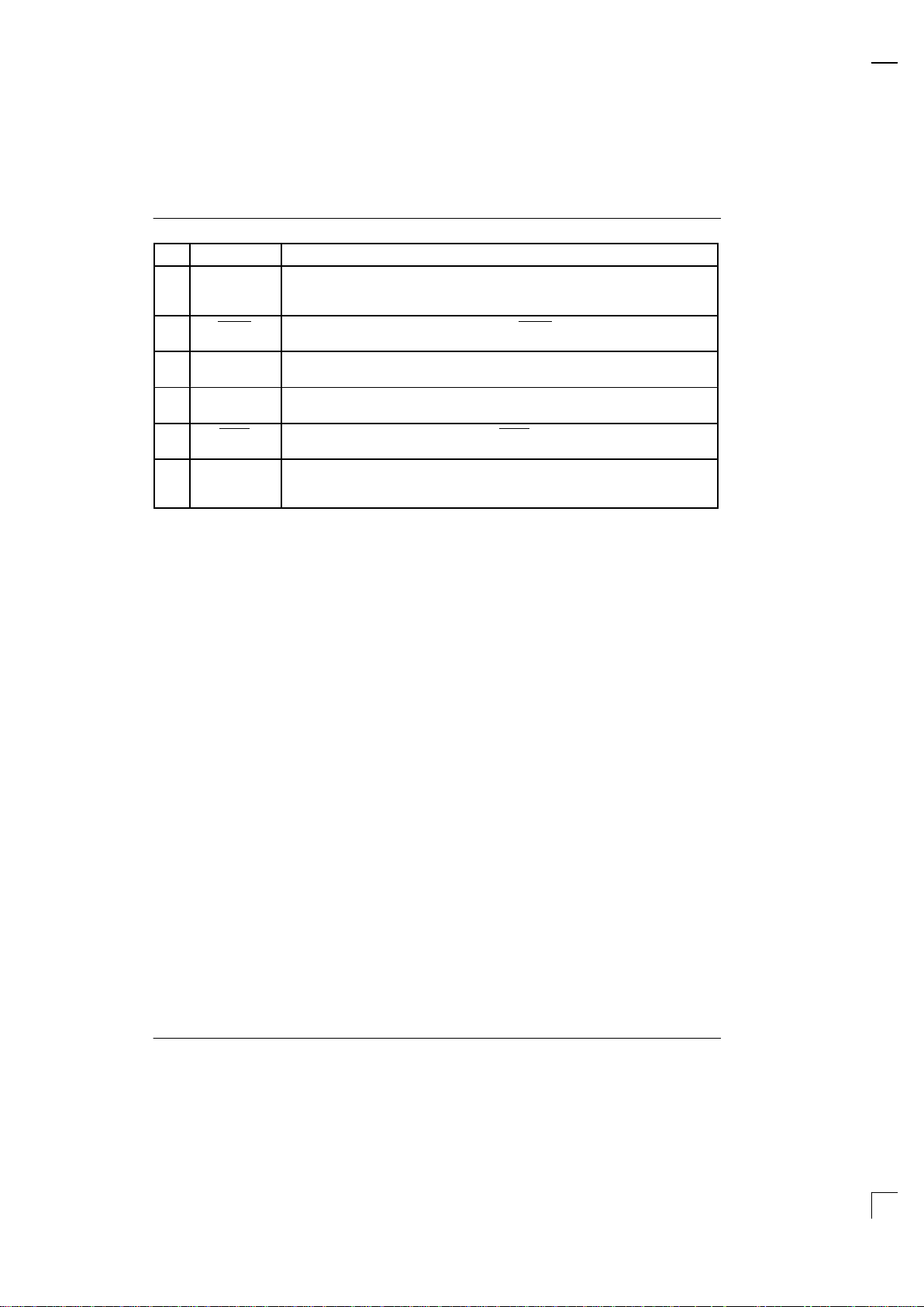
CONTROLLER BLOCK DIAGRAM Figure 1–1
VCC
P7.7 /
AMI.7 /
LED.7
uC
CLK OSC.
VPFW
VRST
GND
XTAL1 XTAL2
PORT 7 /
ACT. MONITOR /
LED CONTROL
P7.0 /
AMI.0 /
LED.0
TIMING /
BUS CONTROL
ALE
PSEN
RST
P3.7 / RD
PORT 3
P3.6 / WR
P3.5 / T1
P3.4 / T0
P3.3 / INT1
P3.2 / INT0
P3.1 / TXD0
P3.0 / RXD0
P1.7
PORT 1
P1.6
P1.3 / SDA1
P1.2 / SCL1
P1.1 / T2EX
P1.0 / T2
P6.7 / SOC
PORT 6 /
P6.6
P6.5 / PWI.1
P6.4 / PWI.0
P6.3 / PWO.3
P6.2 / PWO.2
P6.1 / PWO.1
P6.0 / PWO.0
PWM I/O
P1.5 / SDA2
P1.4 / SCL2
PORT 0
PORT 2
PORT 4 /
KEYBOARD
IN
PORT 8/
KEYBOARD
OUT
P0.7 /
AD7
P0.0 /
AD0
P2.7 /
A15
P2.0 /A8P4.7 /
KSI.7
P4.0 /
KSI.0
P8.7/
KS0.7
P8.0/
KS0.0
P9.7/
KS0.15
P9.0/
KS0.8
PORT 5 /
10–BIT ADC
P5.0 / AI.0
P5.7 / AI.7
AGND
AVCC
VRL
VRH
PM1C
PC I/F
uC I/F
KBC
PC I/F
uC I/F
KBC
OUTPUT
STATUS
KBC
INPUT
SD7–SD0
IOW
IOR
A0
KBCS
KBOBF
SMI1
PM1CS
4 MHz
RING OSC.
SYS. CLOCK
CONTROL
WATCHDOG
TIMER
TIMER 2
TIMER 1
TIMER 0
INT 1
INT 0
8051
UART
ACC. BUS
SIO2
ACC. BUS
SIO1
SCRATCHPAD
REGISTERS
(256 BYTES)
POWER MON./
CONTROL
HVCC
HGND
SPECIAL
HIGH SPEED
256 x 8
FUNCTION
REGISTERS
80C520
CPU CORE
DATA
RAM
POWER
CONTROL
3
3
PORT 9/
KEYBOARD
OUT
P10.7
PORT 10
P10.0
PM1C
PM1C
PM2C
PC I/F
uC I/F
PM2C
PM2C
STATUS
OUTPUT
INPUT
PM2CS
SMI2
STATUS
OUTPUT
INPUT

DS80CH11
011200 7/88
1.2 DETAILED FEATURE SUMMARY
• High Speed 80C32 Compatible Core:
– High performance 4 clocks / machine cycle
(8032 = 12)
– Low Power: typically 1/3 power for equivalent
8032 throughput
– Maximum clock speed up to 25 MHz at 5.0V
– Ultra–low stop mode power (typ. 1 uA) and
“IDLE” mode (typ. 10 mA)
– Multiple wake–up sources from STOP including
key scan, 2–wire, host I/F, or external interrupt
– Three 16–bit timers, 1 serial port
– 256 byte scratchpad
– 256 bytes MOVX RAM
• Keyboard Control:
– Replaces 8042 and key scan microcontroller
– 2 Parallel I/O ports for key scan outputs
– One interrupt–driven 8–bit input port to initiate
key–scan sequence
• Input/Output:
– Total of eleven 8–bit I/O ports; all pins can be
individually programmed to serve as general
purpose digital input/output.
– Each 8–bit port supports one or more special
functions:
Port 0, 2, 3: External program / data memory
interface
Port 1, 3: UART, 2–Wire serial, timers, and
external interrupt I/O.
Port 4, 8, 9: Key scan input / output
Port 5: A/D inputs
Port 6: PWM Outputs
Port 7: Activity monitor, LED Control
Port 10: GPIO
• Analog Input/Output:
– Eight–channel, 10–bit A/D with power down
mode supports charging NiMH rechargeable
cells
– 4–channel, 8–bit PWM supports LCD brightness
and contrast control
• 2–Wire Bi–directional Serial Buses
– Master/slave multi–drop operation
– Manages on–board slaves or external I/O
devices
• Power Control
– Generates system power on reset
– Programmable power down pin states
1.3 CONVENTIONS
The following conventions are used throughout this
specification:
• “SEM” is the short form name used to indicate the
System Energy Manager.
• Signals that are active low are followed by a pound
symbol (#) or backslash (\), or are indicated with an
overbar.
• If a range of signals is described, such as SA0 through
SA10, the range is given as SA10–0, with the most–
significant digit first and the least–significant digit last,
separated by a hyphen.
• Numbers written in this specification can be written as
decimal, hexadecimal, or binary . Hexadecimal numbers are followed by an “H” suffix. Binary numbers are
followed by a “B” suffix. For example, decimal
27 = 1BH = 00011011B.
1.4 ADDITIONAL REFERENCES
The SEM incorporates the Dallas 8051 compatible High
Speed Micro core including the CPU and many of its
core peripherals. The operational details of these elements are contained in the Dallas High Speed Micro
User’s Guide.
DS80CH11
011200 8/88
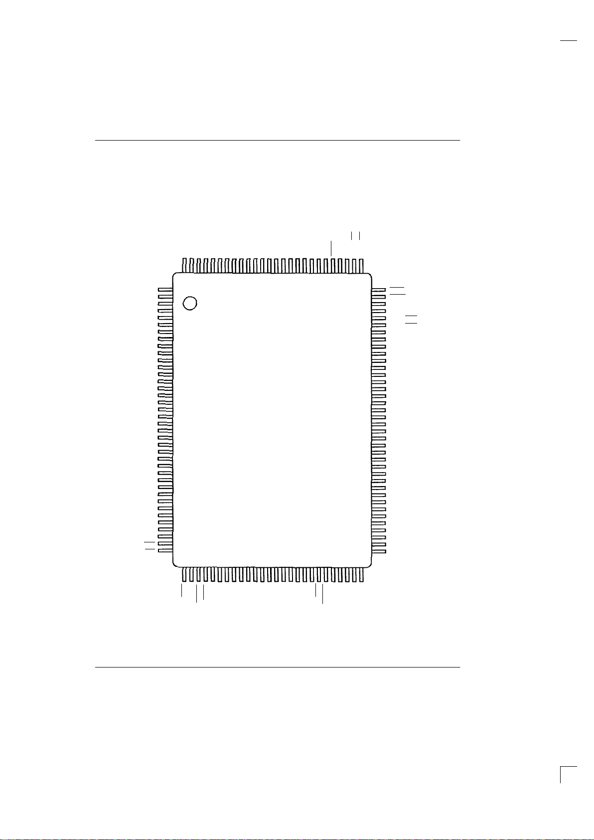
2.0 PIN DESCRIPTION
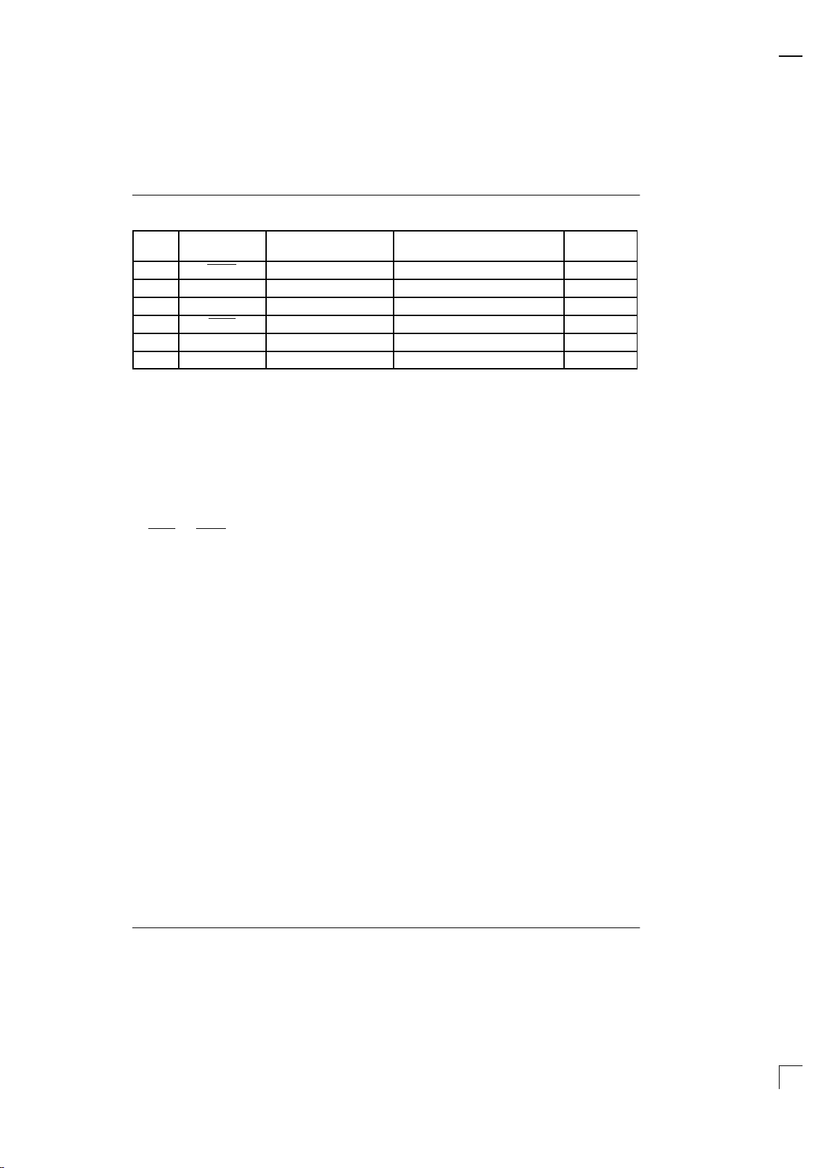
128–TQFP PIN ASSIGNMENT Figure 2–1
VRST
VPFW
P3.5 / T1
P3.4 / T0
P3.3 / INT1
P3.2 / INT0
P3.1 / TXD0
P3.0 / RXD0
P1.7
P1.6
P1.5 / SDA2
P1.4 / SCL2
P1.3 / SDA1
P1.2 / SCL1
P1.1 / T2EX
P1.0 / T2
GND
VCC
P4.7 / KSI.7
P4.6 / KSI.6
P4.5 / KSI.5
P4.4 / KSI.4
P4.3 / KSI.3
P4.2 / KSI.2
P4.1 / KSI.1
P4.0 / KSI.0
P7.7 / AMI.7 / LED.7
P7.6 / AMI.6 / LED.6
P7.5 / AMI.5 / LED.5
P7.4 / AMI.4 / LED.4
P7.3 / AMI.3 / LED.3
P7.2 / AMI.2 / LED.2
P7.1 / AMI.1 / LED.1
P7.0 / AMI.0 / LED.0
HVCC
P10.7
P10.6
P10.5
P9.7 / KSO.15
P9.6 / KSO.14
P9.5 / KSO.13
P9.4 / KSO.12
P9.3 / KSO.11
P9.2 / KSO.10
P9.1 / KSO.9
P9.0 / KSO.8
P8.7 / KSO.7
P8.6 / KSO.6
P8.5 / KSO.5
P8.4 / KSO.4
P8.3 / KSO.3
P8.2 / KSO.2
P8.1 / KSO.1
P8.0 / KSO.0
GND
VCC
P6.7 / SOC
P6.6
P6.5 / PWI.1
P6.4 / PWI.0
P6.3 / PWO.3
P6.2 / PWO.2
P6.1 / PWO.1
P6.0 / PWO.0
P5.7 / AI.7
P5.6 / AI.6
P5.5 / AI.5
P5.4 / AI.4
P5.3 / AI.3
P5.2 / AI.2
P5.1 / AI.1
P5.0 / AI.0
GND
A0
IOW
IOR
1
2
3
4
5
6
7
8
9
10
11
12
13
14
15
16
17
18
19
20
21
22
23
24
25
26
27
28
29
30
31
32
33
34
35
36
37
38
102
101
100
99
98
97
96
95
94
93
92
91
90
89
88
87
86
85
84
83
82
81
80
79
78
77
76
75
74
73
72
71
70
69
68
67
66
65
SMI1
KBOBF
PM1CS
KBCS
AGND
VRH
VRL
AVCC
HGND
SD7
SD6
SD5
SD4
SD3
SD2
SD1
SD0
NC
NC
SMI2
PM2CS
P10.0
P10.1
P10.2
P10.3
P10.4
NC
PSEN
ALE
P0.7 / AD7
P0.6 / AD6
P0.5 / AD5
P0.4 / AD4
P0.3 / AD3
P0.2 / AD2
P0.1 / AD1
P0.0 / AD0
VCC
XTAL2
XTAL1
GND
P2.7 / A15
P2.6 / A14
P2.5 / A13
P2.4 / A12
P2.3 / A1 1
P2.2 / A10
P2.1 / A9
P2.0 / A8
RST
P3.7 / RD
P3.6 / WR
128
127
126
125
124
123
122
121
120
119
118
117
116
115
114
113
112
111
110
109
108
107
106
105
104
103
39404142434445464748495051525354555657585960616263
64
DS80CH11
011200 9/88
2.1 PIN FUNCTION SUMMARY
PIN SYMBOL DESCRIPTION
36 A0 Command / Data Select: Input. Address input used by the host processor in data
transfers to the keyboard controller and power management #1 and #2 interface ports to
indicate whether the transfer is command (A0=1) or data (A0=0).
43 AGND Analog Ground.
106 ALE Address Latch Enable: Output. This signal functions as a clock to latch the external
address LSB from the multiplexed address/data bus on Port 0. This signal is commonly
connected to the latch enable of an external 373 family transparent latch. ALE has a
pulse width of 1.5 XTAL1 cycles and a period of 4 XTAL1 cycles. ALE is forced high
when the SEM is in a Reset condition.
46 AVCC Analog VCC.
17
35
86
117
GND Digital circuit ground.
47 HGND Host Interface Ground:
68 HVCC Host Interface VCC:
38 IOR I/O Read: Input. I/O Read is used to signal a read operation is in effect on the host
address/data bus.
37 IOW I/O Write: Input. I/O Write is used to signal a write operation is in effect on the host
address/data bus.
42 KBCS Keyboard Chip Select: (Input, active low). This is a chip select signal used to enable
the keyboard control host interface port.
40 KBOBF Keyboard Output Buffer Full: (Output, active high). This signal is set when the key-
board control host interface data buffer contains data to be read by the host. KBOBF will
be driven low when host reads the keyboard control data buffer register .
56
57
108
NC No Connection.
121
122
123
124
125
126
127
128
P0.0 (AD0)
P0.1 (AD1)
P0.2 (AD2)
P0.3 (AD3)
P0.4 (AD4)
P0.5 (AD5)
P0.6 (AD6)
P0.7 (AD7)
Port 0 / Address/Data Outputs 7–0: I/O. Port 0 is an open–drain 8–bit bi–directional
I/O port. As an alternate function Port 0 can function as the multiplexed address/data
bus to access off–chip memory . During the time when ALE is high, the LSB of a memory
address is presented. When ALE falls to a logic 0, the port transitions to a bi–directional
data bus. This bus is used to read external ROM and read/write external RAM memory
or peripherals. When used as a memory bus, the port provides active high drivers. The
reset condition of Port 0 is tri–state. Pull–up resistors are required when using Port 0 as
an I/O port.

DS80CH11
011200 10/88
PIN SYMBOL DESCRIPTION
87
88
89
90
91
92
93
94
P1.0 (T2)
P1.1 (T2EX)
P1.2 SCL1
P1.3 SDA1
P1.4 SCL2
P1.5 SDA2
P1.6
P1.7
Port 1/ (Alternate Functions): – I/O. Port 1 provides eight lines which can be individually selected as bi–directional I/O port pins or as the alternate functions listed below:
Alternate
Port
Function Description
P1.0 T2 External I/O for Timer/Counter 2
P1.1 T2EX Timer/Counter 2 Capture/Reload Trigger
P1.2 SCL1 2–Wire Serial Clock 1
P1.3 SDA1 2–Wire Serial Data 1
P1.4 SCL2 2–Wire Serial Clock 2
P1.5 SDA2 2–Wire Serial Data 2
P1.6 (None)
P1.7 (None)
Note that P1.7 – P1.2 are high–drive pins which are always open–drain and must be
used with external pull–ups when used as I/O port pins. P1.1 and P1.0 have internal
pull–up resistors.
109
110
111
112
113
114
115
116
P2.0 (A8)
P2.1 (A9)
P2.2 (A10)
P2.3 (A11)
P2.4 (A12)
P2.5 (A13)
P2.6 (A14)
P2.7 (A15)
Port 2 / Address Outputs A15–8: – I/O. Port 2 is a pseudo–bi–directional I/O port with
internal pull–up resistors. As an alternate function Port 2 can function as MSB of the
external address bus.
95
96
97
98
99
100
103
104
P3.0(RXD0)
P3.1 (TXD0)
P3.2 (INT0
)
P3.3 (INT1
)
P3.4 (T0)
P3.5 (T1)
P3.6 (WR
)
P3.7 (RD
)
Port 3 / (Alternate Functions): – I/O. Port 3 provides eight lines each of which can
serve as psuedo–bi–directional I/O port pins or as the alternate functions as listed
below. Internal pull–up resistors are always present on these pins.
Alternate
Port
Function Description
P3.0 RXD0 Serial Port 0 Input
P3.1 TXD0 Serial Port 0 Output
P3.2 INT0
External Interrupt 0
P3.3 INT1
External Interrupt 1
P3.4 T0 Timer 0 External Input
P3.5 T1 Timer 1 External Input
P3.6 WR
External Data Memory Write Strobe
P3.7 RD
External Data Memory Read Strobe
77
78
79
80
81
82
83
84
P4.0 (KSI.0)
P4.1 (KSI.1)
P4.2 (KSI.2)
P4.3 (KSI.3)
P4.4 (KSI.4)
P4.5 (KSI.5)
P4.6 (KSI.6)
P4.7 (KSI.7)
Port 4 / KSI.7–0: – I/O / Keyboard Scan Inputs. Port 4 provides eight lines which can be
individually selected as psuedo–bi–directional I/O port pins or as an interrupt Inputs for
key scanning. Port 4 pins incorporate Schmitt inputs with pull–up resistors.

DS80CH11
011200 11/88
PIN SYMBOL DESCRIPTION
34
33
32
31
30
29
28
27
P5.0 (AI.0)
P5.1 (AI.1)
P5.2 (AI.2)
P5.3 (AI.3)
P5.4 (AI.4)
P5.5 (AI.5)
P5.6 (AI.6)
P5.7 (AI.7)
Port 5 / AI.7–0: – I/O / A/D inputs. Port 5 provides eight lines which can be individually
selected as open–drain psuedo–bi–directional I/O port pins or as A/D inputs. Pull–up
resistors are required when using Port 5 as an I/O port.
26
25
24
23
22
21
20
19
P6.0 (PWO.0)
P6.1 (PWO.1)
P6.2 (PWO.2)
P6.3 (PWO.3)
P6.4 (PWI.0)
P6.5 (PWI.1)
P6.6
P6.7 / SOC
Port 6 / PW0.3 – 0: – I/O / Pulse–Width Modulated Outputs. Port 6 provides eight lines
which can all serve as psuedo–bi–directional I/O port pins with internal pull–up
resistors. Six lines can be individually selected to serve the pulse–width modulator
function indicated below:
Alternate
Port
Function Description
P6.0 PWO.0 PWM 0 output (active high drive when enabled)
P6.1 PWO.1 PWM 1 output (active high drive when enabled)
P6.2 PWO.2 PWM 2 output (active high drive when enabled)
P6.3 PWO.3 PWM 3 output (active high drive when enabled)
P6.4 PWI.0 Optional clock input for PWM channels 0 and 2
P6.5 PWI.1 Optional clock input for PWM channels 1 and 3
P6.6 (none)
P6.7 SOC External A / D start of conversion signal
69
70
71
72
73
74
75
76
P7.0 (AMI.0)
(LED.0)
P7.1 (AMI.1)
(LED.1)
P7.2 (AMI.2)
(LED.2)
P7.3 (AMI.3)
(LED.3)
P7.4 (AMI.4)
(LED.4)
P7.5 (AMI.5)
(LED.5)
P7.6 (AMI.6)
(LED.6)
P7.7 (AMI.7)
(LED.7)
Port 7 / AMI.7–0 / LED.7–0: – I/O / Activity Monitor Inputs / LED Control. Port 7 provides
eight lines which can serve as a psuedo–bi–directional I/O port pins with internal pull–
ups or as Activity Monitor inputs. When used as Activity Monitor inputs, these pins are
typically connected to the chip select line of an external peripheral device, and can be
programmed to sense active–high or active–low signals. Any pin which is programmed
as an Activity Monitor input by setting its AMEn bit to a 1 will have its pull–up device disabled and thereby function as an open–drain
pin in order to eliminate unnecessary cur-
rent drain. All port 7 pins are capable of controlling LED’s.
16
15
14
13
12
11
10
9
P8.0 (KSO.0)
P8.1 (KSO.1)
P8.2 (KSO.2)
P8.3 (KSO.3)
P8.4 (KSO.4)
P8.5 (KSO.5)
P8.6 (KSO.6)
P8.7 (KSO.7)
Port 8 / KSO.7–0:– I/O. Port 8 provides eight lines of open–drain psuedo–bi–directional
I/O port pins. Typically, these lines are used for key–scan outputs.
DS80CH11
011200 12/88
PIN SYMBOL DESCRIPTION
8
7
6
5
4
3
2
1
P9.0 (KSO.8)
P9.1 (KSO.9)
P9.2 (KSO.10)
P9.3 (KSO.11)
P9.4 (KSO.12)
P9.5 (KSO.13)
P9.6 (KSO.14)
P9.7 (KSO.15)
Port 9 / KSO.15–8: – I/O. Port 9 provides eight lines of open–drain psuedo–bi–directional I/O port pins. Typically, these lines are used for key–scan outputs.
60
61
62
63
64
65
66
67
P10.0
P10.1
P10.2
P10.3
P10.4
P10.5
P10.6
P10.7
Port10: –I/O. Port 10 provides eight lines of general purpose Input or Output.
41 PM1CS Power Management #1 Chip Select: (Input, active low). This is a chip select signal
used to enable the power management #1 host interface port.
59 PM2CS Power Management #2 Chip Select: (Input, active low). This is a chip select signal
used to enable the power management #2 host interface port.
107 PSEN Program Store Enable: Output. This signal goes low when off–chip program memory
is being accessed via Ports 0 and 2. It is commonly connected to optional external ROM
memory as a chip enable. PSEN
will provide an active low pulse and is driven high when
external ROM is not being accessed.
105 RST Reset: Input, active high The RST input pin contains a Schmitt voltage input to recog-
nize external active high Reset inputs. The pin also employs an internal pull–down
resistor to allow for a combination of wired OR external Reset sources. An RC is not
required for power–up, as the controller provides this function internally.
55
54
53
52
51
50
49
48
SD0
SD1
SD2
SD3
SD4
SD5
SD6
SD7
System Data Bus: (Bi–directional). SD7–0 are data bus lines used for data transfers
between the host processor and the keyboard interface buffer and power management
#1 and #2 interface buffers.
39 SMI1 System Management Interrupt #1: (Output, active low). This signal is driven low
when the power management #1 host interface data buffer contains data to be read by
the host. SMI1
will be returned to a High Level when host reads the power management
#1 data buffer register.
58 SMI2 System Management Interrupt #2: (Output, active low). This signal is driven low
when the power management #2, host interface data buffer contains data to be read by
the host. SMI2
will be returned to a high level when the host reads the power manage-
ment #2 data buffer register .
DS80CH11
011200 13/88
PIN SYMBOL DESCRIPTION
18
85
120
VCC Digital Power Supply Input: For microcontroller and associated functions.
101 VPFW Power Fail Warning: Output, active low. The VPFW pin signals an impending power
failure when VCC drops below VPFW voltage threshold.
44 VRH A/D Positive Voltage Reference: The VRH pin is the positive reference (upper voltage
limit) of the A/D Converter.
45 VRL A/D Negative Voltage Reference: The VRL pin is the negative reference (lower volt-
age limit) of the A/D Converter.
102 VRST Power Fail Reset: Output, active low. The VRST pin signals a “power not good” condi-
tion to the system when system VCC has dropped below the VRST voltage threshold.
118
119
XTAL1
XTAL2
µC Crystal Oscillator Inputs. XTAL1 and XT AL2 provide support for parallel resonant,
AT cut crystals. XT AL1 acts also as an input if there is an external clock source in place
of a crystal. XTAL2 serves as the output of the crystal amplifier.

DS80CH11
011200 14/88
2.2 PIN CHARACTERISTICS
PIN NAME
POWER DOWN
MODE STATE
I/O BUFFER TYPE
RESET
STATE
36 A0 – I –
43 AGND – – –
106 ALE Low O Low
46 AVCC – – –
17 GND – – –
35 GND – – –
86 GND – – –
117 GND – – –
47 HGND – – –
68 HVCC – – –
38 IOR – I –
37 IOW – I –
42 KBCS – I –
40 KBOBF Hold O Low
57 NC – – –
56 NC – – –
108 NC – – –
121 P0.0 / AD0 High–Z Open–Drain (port)
CMOS drive (bus)
High–Z
122 P0.1 / AD1 High–Z Open–Drain (port)
CMOS drive (bus)
High–Z
123 P0.2 / AD2 High–Z Open–Drain (port)
CMOS drive (bus)
High–Z
124 P0.3 / AD3 High–Z Open–Drain (port)
CMOS drive (bus)
High–Z
125 P0.4 / AD4 High–Z Open–Drain (port)
CMOS drive (bus)
High–Z
126 P0.5 / AD5 High–Z Open–Drain (port)
CMOS drive (bus)
High–Z
127 P0.6 / AD6 High–Z Open–Drain (port)
CMOS drive (bus)
High–Z
128 P0.7 / AD7 High–Z Open–Drain (port)
CMOS drive (bus)
High–Z
87 P1.0 / T2 Hold Pull–up Weak High
88 P1.1 / T2EX Hold Pull–up Weak High
89 P1.2 / SCL1 Hold Open–drain High–Z
90 P1.3 / SDA1 Hold Open–drain High–Z

DS80CH11
011200 15/88
2.2 PIN CHARACTERISTICS (cont’d)
PIN NAME
POWER DOWN
MODE STATE
I/O BUFFER TYPE
RESET
STATE
91 P1.4 /SCL2 Hold Open–drain High–Z
92 P1.5 /SDA2 Hold Open–drain High–Z
93 P1.6 Hold Open–drain High–Z
94 P1.7 Hold Open–drain High–Z
109 P2.0 / A8 Hold Pull–up Weak High
110 P2.1 / A9 Hold Pull–up Weak High
111 P2.2 / A10 Hold Pull–up Weak High
112 P2.3 / A11 Hold Pull–up Weak High
113 P2.4 / A12 Hold Pull–up Weak High
114 P2.5 / A13 Hold Pull–up Weak High
115 P2.6 / A14 Hold Pull–up Weak High
116 P2.7 / A15 Hold Pull–up Weak High
95 P3.0 / RXD0 Hold Pull–up Weak High
96 P3.1 / TXD0 Hold Pull–up Weak High
97 P3.2 / INT0 Hold Pull–up Weak High
98 P3.3 / INT1 Hold Pull–up Weak High
99 P3.4 / T0 Hold Pull–up Weak High
100 P3.5 / T1 Hold Pull–up Weak High
103 P3.6 / WR Hold Pull–up Weak High
104 P3.7 / RD Hold Pull–up Weak High
77 P4.0 / KSI.0 Hold Pull–up Weak High
78 P4.1 / KSI.1 Hold Pull–up Weak High
79 P4.2 / KSI.2 Hold Pull–up Weak High
80 P4.3 / KSI.3 Hold Pull–up Weak High
81 P4.4 / KSI.4 Hold Pull–up Weak High
82 P4.5 / KSI.5 Hold Pull–up Weak High
83 P4.6 / KSI.6 Hold Pull–up Weak High
84 P4.7 / KSI.7 Hold Pull–up Weak High
34 P5.0 / AI.0 Hold Open–drain High–Z
33 P5.1 / AI.1 Hold Open–drain High–Z
32 P5.2 / AI.2 Hold Open–drain High–Z
31 P5.3 / AI.3 Hold Open–drain High–Z

DS80CH11
011200 16/88
2.2 PIN CHARACTERISTICS (cont’d)
PIN NAME
POWER DOWN
MODE STATE
I/O BUFFER TYPE
RESET
STATE
30 P5.4 / AI.4 Hold Open–drain High–Z
29 P5.5 / AI.5 Hold Open–drain High–Z
28 P5.6 / AI.6 Hold Open–drain High–Z
27 P5.7 / AI.7 Hold Open–drain High–Z
26 P6.0 / PWO.0 Hold Pull–up (PWMn disabled)
CMOS drive (PWMn enabled)
Weak High
25 P6.1 / PWO.1 Hold Pull–up (PWMn disabled)
CMOS drive (PWMn enabled)
Weak High
24 P6.2 / PWO.2 Hold Pull–up (PWMn disabled)
CMOS drive (PWMn enabled)
Weak High
23 P6.3 / PWO.3 Hold Pull–up (PWMn disabled)
CMOS drive (PWMn enabled)
Weak High
22 P6.4 / PWI.0 Hold Pull–up Weak High
21 P6.5 / PWI.1 Hold Pull–up Weak High
20 P6.6 Hold Pull–up Weak High
19 P6.7 / SOC Hold Pull–up Weak High
69 P7.0 / AMI.0 /
LED.0
Hold Pull–up Weak High
70 P7.1 / AMI.1 /
LED.1
Hold Pull–up Weak High
71 P7.2 / AMI.2 /
LED.2
Hold Pull–up Weak High
72 P7.3 / AMI.3 /
LED.3
Hold Pull–up Weak High
73 P7.4 / AMI.4/
LED.4
Hold Pull–up Weak High
74 P7.5 / AMI.5/
LED.5
Hold Pull–up Weak High
75 P7.6 / AMI.6/
LED.6
Hold Pull–up Weak High
76 P7.7 / AMI.7/
LED.7
Hold Pull–up Weak High
16 P8.0 / KSO.0 Hold Open–drain High–Z
15 P8.1 / KSO.1 Hold Open–drain High–Z
14 P8.2 / KSO.2 Hold Open–drain High–Z
13 P8.3 / KSO.3 Hold Open–drain High–Z
12 P8.4 / KSO.4 Hold Open–drain High–Z
11 P8.5 / KSO.5 Hold Open–drain High–Z
10 P8.6 / KSO.6 Hold Open–drain High–Z

DS80CH11
011200 17/88
2.2 PIN CHARACTERISTICS (cont’d)
PIN NAME
POWER DOWN
MODE STATE
I/O BUFFER TYPE
RESET
STATE
9 P8.7 / KSO.7 Hold Open–drain High–Z
8 P9.0 / KSO.8 Hold Open–drain High–Z
7 P9.1 / KSO.9 Hold Open–drain High–Z
6 P9.2 / KSO.10 Hold Open–drain High–Z
5 P9.3 / KSO.11 Hold Open–drain High–Z
4 P9.4 / KSO.12 Hold Open–drain High–Z
3 P9.5 / KSO.13 Hold Open–drain High–Z
2 P9.6 / KSO.14 Hold Open–drain High–Z
1 P9.7 / KSO.15 Hold Open–drain High–Z
60 P10.0 Hold Pull–up Weak High
61 P10.1 Hold Pull–up Weak High
62 P10.2 Hold Pull–up Weak High
63 P10.3 Hold Pull–up Weak High
64 P10.4 Hold Pull–up Weak High
65 P10.5 Hold Pull–up Weak High
66 P10.6 Hold Pull–up Weak High
67 P10.7 Hold Pull–up Weak High
41 PM1CS – I –
59 PM2CS – I –
107 PSEN Low O Low
105 RST – I –
55 SD0 (note 2) Bi–directional (note 2)
54 SD1 (note 2) Bi–directional (note 2)
53 SD2 (note 2) Bi–directional (note 2)
52 SD3 (note 2) Bi–directional (note 2)
51 SD4 (note 2) Bi–directional (note 2)
50 SD5 (note 2) Bi–directional (note 2)
49 SD6 (note 2) Bi–directional (note 2)
48 SD7 (note 2) Bi–directional (note 2)
39 SMI1 Hold O High
58 SMI2 Hold O High
18 VCC – – –
85 VCC – – –
120 VCC – – –
DS80CH11
011200 18/88
2.2 PIN CHARACTERISTICS (cont’d)
PIN NAME
POWER DOWN
MODE STATE
I/O BUFFER TYPE
RESET
STATE
101 VPFW (note 3) O (note 3)
44 VRH – – –
45 VRL – – –
102 VRST (note 3) O (note 3)
118 XTAL1 – I –
119 XTAL2 H O –
PIN STATE DESCRIPTIONS
High–Z High Impedance
Enabled Power applied; electrically functioning input
Unchanged Previous state not affected
NOTES:
1. As shown above, the original port pins P1.7–P1.2 have been modified to open–drain instead of having “Internal”
pull–up resistors.
2. This signal is independently powered from the HVCC on pin 68. As a result, the state of the reset pin and the power
down mode have no effect on its operation.
3. VRST
and VPFW reflects the state of VCC with respect to the power–fail reset and power–fail warning trip points,
respectively, and is unaf fected by the RST pin and power down mode state.

DS80CH11
011200 19/88
3.0 CORE MICROCONTROLLER
3.1 CORE MICRO OVERVIEW
The SEM incorporates the Dallas High Speed Micro
core which is a fully static CMOS 8051 compatible
microcontroller with a new internal architecture
designed for high performance. The higher speed
operation of the microcontroller core comes not just
from increasing the clock frequency, but from a newer,
more efficient design of the internal architecture. The
major features of the High Speed Micro Core include:
• 4 clocks/machine cycle (8032 = 12)
• Wasted cycles removed
• Runs DC to 25 Mhz clock rates @ 5V
• Single–cycle instruction in 160 ns
• Uses less power for equivalent work
• Dual data pointer
• Optional variable length MOVX to access fast/slow
RAM /peripherals
3.2 INSTRUCTION SET SUMMARY
All instructions in the SEM perform the same functions
as their 80C32 counterparts. Their affect on bits, flags,
and other status functions are identical. However, the
timing of each instruction is different. This applies both
in absolute and relative number of clocks.
For absolute timing of real–time events, the timing of
software loops will need to be calculated using the table
below. However, counter/timers default to run at the
older 12 clocks per increment. Therefore, while software runs at higher speed, timer–based events need no
modification to operate as before. Timers can be set to
run at 4 clocks per increment cycle to take advantage of
higher speed operation.
The relative time of two instructions might be different in
the new architecture than it was previously. For example, in the original architecture, the “MOVX A, @ DPTR”
instruction and the “MOV direct, direct” instruction used
two machine cycles or 24 oscillator cycles. Therefore,
they required the same amount of time. In the GEM, the
MOVX instruction can be done in two machine cycles or
8 oscillator cycles but the “MOV direct, direct” uses
three machine cycles or 12 oscillator cycles. While both
are faster than their original counterparts, they now
have different execution times from each other. This is
because in most cases, the SEM uses one cycle for
each byte. The timing of each instruction should be
examined for familiarity with the changes. Note that a
machine cycle now requires just four clocks, and provides one ALE pulse per cycle. Many instructions
require only one cycle, but some require five. In the original architecture, all were one or two cycles except for
MUL and DIV.
INSTRUCTION SET SUMMARY Table 3–1
Legends:
A – Accumulator
Rn – Register R7–R0
direct – Internal Register address
@Ri – Internal Register pointed–to by R0 or R1
(except MOVX)
rel – 2’s complement offset byte
bit – direct bit–address
#data – 8–bit constant
#data 16 – 16–bit constant
addr 16 – 16–bit destination address
addr 11 – 11–bit destination address

DS80CH11
011200 20/88
INSTRUCTION SET SUMMARY Table 3–1 (cont’d)
INSTRUCTION BYTE
OSCILLATOR
CYCLES
INSTRUCTION BYTE
OSCILLATOR
CYCLES
Arithmetic Instructions:
ADD A, Rn 1 4 INC A 1 4
ADD A, direct 2 8 INC Rn 1 4
ADD A, @Ri 1 4 INC direct 2 8
ADD A, #data 2 8 INC @Ri 1 4
ADDC A, Rn 1 4 INC DPTR 1 12
ADDC A, direct 2 8 DEC A 1 4
ADDC A, @Ri 1 4 DEC Rn 1 4
ADDC A, #data 2 8 DEC direct 2 8
SUBB A, Rn 1 4 DEC @Ri 1 4
SUBB A, direct 2 8 MUL AB 1 20
SUBB A, @Ri 1 4 DIV AB 1 20
SUBB A, #data 2 8 DA A 1 4
Logical Instructions:
ANL A, Rn 1 4 XRL A, Rn 1 4
ANL A, direct 2 8 XRL A, direct 2 8
ANL A, @Ri 1 4 XRL A, @Ri 1 4
ANL A, #data 2 8 XRL A, #data 2 8
ANL direct, A 2 8 XRL direct, A 2 8
ANL direct, #data 3 12 XRL direct, #data 3 12
ORL A, Rn 1 4 CLR A 1 4
ORL A, direct 2 8 CPL A 1 4
ORL A, @Ri 1 4 RL A 1 4
ORL A, #data 2 8 RLC A 1 4
ORL direct, A 2 8 RR A 1 4
ORL direct, #data 3 12 RRC A 1 4
SWAP A 1 4
Data Transfer
Instructions:
MOV A, Rn 1 4 MOVC A, @A+DPTR 1 12
MOV A, direct 2 8 MOVC A, @A+PC 1 12
MOV A, @Ri 1 4 MOVX A, @Ri 1 8–36
MOV A, #data 2 8 MOVX A, @DPTR 1 8–36
MOV Rn, A 1 4 MOVX @Ri, A 1 8–36
MOV Rn, direct 2 8 MOVX @DPTR, A 1 8–36
MOV Rn, #data 2 8 PUSH direct 2 8
MOV direct, A 2 8 POP direct 2 8
MOV direct, Rn 2 8 XCH A, Rn 1 4
MOV direct1, direct2 3 12 XCH A, direct 2 8
MOV direct, @Ri 2 8 XCH A, @Ri 1 4
MOV direct, #data 3 12 XCHD A, @Ri 1 4
MOV @Ri, A 1 4
MOV @Ri, direct 2 8
MOV @Ri, #data 2 8
MOV DPTR, #data 16 3 12

DS80CH11
011200 21/88
INSTRUCTION SET SUMMARY Table 3–1 (cont’d)
Bit Manipulation
Instructions:
CLR C 1 4 ANL C, bit 2 8
CLR bit 2 8 ANL C, bit
28
SETB C 1 4 ORL C, bit 2 8
SETB bit 2 8 ORL C, bit
28
CPL C 1 4 MOV C, bit 2 8
CPL bit 2 8 MOV bit, C 2 8
Program Branching
Instructions:
ACALL addr 11 2 12 CJNE A, direct, rel 3 16
LCALL addr 16 3 16 CJNE A, #data, rel 3 16
RET 1 16 CJNE Rn, #data, rel 3 16
RETI 1 16 CJNE @ Ri, #data, rel 3 16
AJMP addr 11 2 12 NOP 1 4
LJMP addr 16 3 16 JC rel 2 12
SJMP rel 2 12 JNC rel 2 12
JMP @A+DPTR 1 12 JB bit, rel 3 16
JZ rel 2 12 JNB bit, rel 3 16
JNZ rel 2 12 JBC bit, rel 3 16
DJNZ Rn, rel 2 12
DJNZ direct, rel 3 16
The Table above shows the speed for each class of
instruction. Note that many of the instructions have multiple opcodes. There are 255 opcodes for 111 instructions. Of the 255 opcodes, 159 are three times faster
than the original 80C32. While a system than emphasizes those instructions will see the most improvement,
the large total number that receive a three to one
improvement assure a dramatic speed increase for any
system. The speed improvement summary is provided
below.
3.3 SPEED IMPROVEMENT
The following table summarizes the speed improvement of the High Speed Micro core over a standard 12
clock / machine cycle 8052 device.
#Opcodes Speed Improvement
159 3.0 x
51 1.5 x
43 2.0 x
2 2.4 x
255 Average: 2.5
3.4 INSTRUCTION SET ADDITIONAL
REFERENCES
The user should refer to the Dallas High Speed Micro
User’s Guide for a complete description of the instruction set including its address modes, coding, and timing
for the SEM.
3.5 RESET
The High–Speed Micro has three ways of entering a
reset state:
• Power–On / Fail Reset
• Watchdog Timer Reset
• External Reset
The operation of the CPU timing and states during a
reset are documented in the Dallas High Speed Micro
User’s Guide under the “Reset Conditions” section. The
Watchdog Timer reset is documented in the Watchdog
Timer section of the Dallas High Speed Micro User’s
Guide. The operation of the Power–On / Fail reset is
described in the Power Management section of this document.
DS80CH11
011200 22/88
3.6 INTERRUPT CONTROL
The SEM provides 16 sources of interrupt with three
priority levels. The Power–fail Interrupt (PFI), if
enabled, always has the highest priority . There are two
remaining user selectable priorities: high and low. If two
interrupts that have the same priority occur simulta-
neously, the hardware–determined precedence given
below determines which is a acted upon. Except for the
PFI, all interrupts that are new to the 8051 family have a
lower natural priority than the originals.
INTERRUPT PRIORITY Table 3–2
NAME DESCRIPTION VECTOR
NATURAL
PRIORITY
8051/DALLAS
PFI Power Fail Interrupt 33h 1 DALLAS
INT0 External Interrupt 0 03h 2 8051
TF0 Timer 0 0Bh 3 8051
INT1 External Interrupt 1 13h 4 8051
TF1 Timer 1 1Bh 5 8051
SCON0 TI0 or RI0 from Serial Port 0 23h 6 8051
TF2 Timer 2 2Bh 7 8051
AMI Activity Monitor Interrupt 3Bh 8 DALLAS
2WI1 2–Wire Serial Port 1 43h 9 DALLAS
ADI A/D End of Conversion 4Bh 10 DALLAS
2WI2 2–Wire Serial Port 2 53h 11 DALLAS
KBI Keyboard Buffer Input 5Bh 12 DALLAS
PBI1 Power Mgmt. Buffer Input #1 63h 13 DALLAS
KDI Key Detect Input 6Bh 14 DALLAS
WDI WatchDog Periodic Interrupt 73h 15 DALLAS
PBI2 Power Mgmt. Buffer Input #2 7Bh 16 DALLAS
INTERRUPT CONTROL SUMMARY Table 3–3
INTERRUPT
SOURCE
FLAG(S)
FLAG
LOC.
ENABLE
ENABLE
LOC.
PRIORITY
PRIORITY
LOC.
Power Fail PFI WDCON.4 EPFI WDCON.5 N/A N/A
External 0 IE0 TCON.1 EX0 IE.0 PX0 IP.0
Timer 0 TF0 TCON.5 ET0 IE.1 PT0 IP.1
External 1 IE1 TCON.3 EX1 IE.2 PX1 IP.2
Timer 1 TF1 TCON.7 ET1 IE.3 PT1 IP.3
Serial Port 0 RI0,TI0 SCON0.0/
SCON0.1
ES0 IE.4 PS0 IP.4
Timer 2 TF2 T2CON.7 ET2 IE.5 PT2 IP.5
Activity monitor AMF7–0 AMF.7–0 EAM IE.6 PAM IP.6
DS80CH11
011200 23/88
INTERRUPT CONTROL SUMMARY Table 3–3 (cont’d)
INTERRUPT
SOURCE
FLAG(S)
FLAG
LOC.
ENABLE
ENABLE
LOC.
PRIORITY
PRIORITY
LOC.
2–Wire Serial Port 1 2WIF1 2WCON1.4 E2W1 EIE.0 P2W1 EIP.0
A/D End of Conv. EOC ADCON1.6 EAD EIE.1 PAD EIP.1
2–Wire Serial Port 2 2WIF2 2WCON2.4 E2W2 EIE.2 P2W2 EIP.2
Keyboard Buffer KIBF KBSTAT.1 EKB EIE.3 PKB EIP.3
Power Mgmt. #1 Buffer PIBF1 PMSTAT1.1 EPB1 EIE.4 PPB1 EIP.4
Key Detect Input KDF7–0 KDF.7–0 EKD EIE.5 PKD EIP.5
WatchDog periodic WDIF WDCON.3 EWDI EIE.6 PWDI EIP.6
Power Mgmt. #2 Buffer PIBF2 PMSTAT2.1 EPB2 EIE.7 PPB2 EIP.7
A complete description of the interrupt structure of the microcontroller core including operation of the priority scheme
and acknowledgment operation is contained in the Dallas High Speed Micro User’s Guide.
DS80CH11
011200 24/88
4.0 MEMORY RESOURCES
4.1 OVERVIEW
The SEM contains the following memory resources and
features:
• 256 bytes of on–chip direct (scratchpad) RAM
• 256 bytes of on–chip MOVX data RAM
• Off–chip program and data memory expansion
• Software enable/disable of on–chip data memory
4.2 DATA MEMORY ACCESS
Unlike many 8051 derivatives, the SEM contains on–
chip data memory. Although physically on–chip, software accesses this area in the same way off–chip data
memory is accessed: via the MOVX instruction. The
256 bytes of SRAM is located between address 0000h
and 00FFh.
Access to the on–chip data RAM is optional under software control. When enabled by software, the data
SRAM is between 0000h and 00FFh. Any MOVX
instruction that uses this area will go to the on–chip RAM
while enabled. MOVX addresses greater than 256
automatically go to external memory through Ports
0 & 2.
When disabled, the 256 bytes of memory area is transparent to the system memory map. Any MOVX directed
to the space between 0000h and FFFFh goes to the
expanded bus on Ports 0 & 2. This also is the default
condition. This default allows the SEM to drop into an
existing system that uses these addresses for other
hardware and still have full compatibility.
The on–chip data area is selected by software using two
bits in the Power Management Register at location C4h.
This selection is dynamically programmable. Thus
access to the on–chip area becomes transparent to
reach off–chip devices at the same addresses. The
control bits are DME1 (PMR.1) and DME0 (PMR.0).
Their operation is described in Table 4–1.
DATA MEMORY ACCESS CONTROL Table 4–1
DME1 DME0 DATA MEMORY ADDRESS MEMORY FUNCTION
0 0 0000h – FFFFh External Data Memory (Default condition)
0 1 0000h – 00FFh
0100h – FFFFh
Internal SRAM Data Memory
External Data Memory
1 0 Reserved Reserved
1 1 0000h – 00FFh
0100h – FFFBh
FFFCh
FFFDh – FFFFh
Internal SRAM Data Memory
Reserved – no external access
Read access to the status of lock bits
Reserved – no external access
Notes on the status byte read at FFFCh with DME1, 0 = 1, 1: Bits 2–0 reflect the programmed status of the security
lock bits LB3–LB1. They are individually set to a logic 1 to correspond to a security lock bit that has been programmed.
These status bits allow software to verify that the part has been locked before running if desired. The bits are read
only.
4.2.1 Stretch Memory Cycle
The SEM allows software to adjust the speed of off–chip
data memory access. The micro is capable of performing the MOVX in as little as two instruction cycles. The
on–chip SRAM uses this speed and any MOVX instruction directed internally uses two cycles. However, the
time can be stretched for interface to external devices.
This allows access to both fast memory and slow
memory or peripherals with no glue logic. Even in high–
speed systems, it may not be necessary or desirable to
perform off–chip data memory access at full speed. In
addition, there are a variety of memory mapped peripherals such as LCDs or UARTs that are slow.
Operation of the Stretch MOVX function is fully documented in the Dallas High Speed Micro User’s Guide.

DS80CH11
011200 25/88
4.2.2 Dual Data Pointer
A second data pointer register (DPTR 1) is incorporated
into the SEM in addition to the standard one in the 8051.
This feature allows faster execution of many operations
involving data memory access, such as block moves.
Operation of the dual data pointer function is fully documented in the Dallas High Speed Micro User’s Guide.
4.3 EXTERNAL MEMORY INTERFACE
Interface techniques for interfacing external memory as
program or data storage to the SEM via Ports 0 and 2
are described in the Dallas High Speed Micro User’s
Guide.
4.4 DIRECT (SCRATCHPAD) RAM ACCESS
The SEM incorporates a full 256 bytes of direct RAM.
This RAM is accessed in a manner identical to that of a
standard 80C52 compatible device. A full description of
this memory along with the instructions that access it is
contained in the Dallas High Speed Micro User’s Guide.
4.5 SPECIAL FUNCTION REGISTERS
Special Function Registers (SFRs) control most special
features of the SEM. This allows the SEM to have many
new features but use the same instruction set as the
8051. When writing software to use a new feature, an
equate statement defines the SFR to an assembler or
compiler. This is the only change needed to access the
new function. The SEM duplicates the SFRs contained
in the standard 80C52. Table 4–2 is a summary of the
values loaded into the SEM’s SFR’s on reset. T able 4–3
is a summary of all of the SFR’s and the control bits they
contain.

F8h
F0h
E8h
E0h
D8h
D0h
C8h
C0h
B8h
B0h
A8h
A0h
98h
90h
88h
80h
DS80CH11
011200 26/88
SPECIAL FUNCTION REGISTER RESET VALUES Table 4–2
* New functions are in bold
EIP
00000000
B
00000000
PORT10
11111111
PMSTAT2
XXXXXX00
PMDIN2
XXXXXXXX
PMDOUT2
XXXXXXXX
EIE
00000000
PORT9
11111111
PW23CON
00000000
PWM2
00000000
PWM3
00000000
ACC
00000000
PORT8
11111111
PW23CS
00000000
PW2FG
00000000
PW3FG
00000000
WDCON
0X0X0XX0
2WCON2
00000000
2WSTAT12
00000000
2WSTAT22
00000000
PW01CON
00000000
PWM0
00000000
PWM1
00000000
PSW
00000000
2WSADR2
00000000
2WDAT2
00000000
2WFS2
00000000
PORT7
11111111
PW01CS
00000000
PW0FG
00000000
PW1FG
00000000
T2CON
00000000
T2MOD
11111100
RCAP2L
00000000
RCAP2H
00000000
TL2
00000000
TH2
00000000
PMR
010X0000
STATUS
00000000
TA
11111111
IP
10000000
SADEN0
00000000
PORT6
11111111
PMSTAT1
XXXXXX00
PMDIN1
XXXXXXXX
PMDOUT1
XXXXXXXX
PORT3
11111111
ADCON1
00000000
ADCON2
00000000
ADMSB
00000000
ADLSB
00000000
WINHI
00000000
WINLO
00000000
IE
00000000
SADDR0
00000000
PORT5
11111111
KBSTAT
XXXXXX00
KBDIN
XXXXXXXX
KBDOUT
XXXXXXXX
PORT2
11111111
PORT4
11111111
KDE
00000000
KDF
00000000
SCON0
00000000
SBUF0
00000000
2WSADR1
00000000
2WDAT1
00000000
2WFS1
00000000
2WCON1
00000000
2WSTAT11
00000000
2WSTAT21
00000000
PORT1
11111111
EXIF
0000XXX0
AME
00000000
AMQ
00000000
AMP
00000000
AMF
00000000
TCON
00000000
TMOD
00000000
TL0
00000000
TL1
00000000
TH0
00000000
TH1
00000000
CKCON
00000001
PORT0
11111111SP000001 11
DPL
00000000
DPH
00000000
DPL1
00000000
DPH1
00000000
DPS
00000000
PCON
00110000
FFh
F7h
EFh
E7h
DFh
D7h
CFh
C7h
BFh
B7h
AFh
A7h
9Fh
97h
8Fh
87h
DS80CH11
011200 27/88
SPECIAL FUNCTION REGISTER LOCATIONS Table 4–3
* New functions are in bold
REGISTER BIT 7 BIT 6 BIT 5 BIT 4 BIT 3 BIT 2 BIT 1 BIT 0 ADDRESS
PORT0 P0.7 P0.6 P0.5 P0.4 P0.3 P0.2 P0.1 P0.0 80h
SP 81h
DPL 82h
DPH 83h
DPL1 84h
DPH1 85h
DPS 0 0 0 0 0 0 0 SEL 86h
PCON SMOD SMOD0 – – GF1 GF0 STOP IDLE 87h
TCON TF1 TR1 TF0 TR0 IE1 IT1 IE0 IT0 88h
TMOD GATE C/T M1 M0 GATE C/T M1 M0 89h
TL0 8Ah
TL1 8Bh
TH0 8Ch
TH1 8Dh
CKCON WD1 WD0 T2M T1M T0M MD2 MD1 MD0 8Eh
PORT1 P1.7 P1.6 P1.5 P1.4 P1.3 P1.2 P1.1 P1.0 90h
EXIF – – – – XT/RG RGMD RGSL BGS 91h
AME AME7 AME6 AME5 AME4 AME3 AME2 AME1 AME0 92h
AMQ AMQ7 AMQ6 AMQ5 AMQ4 AMQ3 AMQ2 AMQ1 AMQ0 93h
AMP AMP7 AMP6 AMP5 AMP4 AMP3 AMP2 AMP1 AMP0 94h
AMF AMF7 AMF6 AMF5 AMF4 AMF3 AMF2 AMF1 AMF0 95h
SCON0 SM0/FE SM1 SM2 REN TB8 RB8 TI0 RI0 98h
SBUF0 SB7 SB6 SB5 SB4 SB3 SB2 SB1 SB0 99h
2WSADR1 SLA6 SLA5 SLA4 SLA3 SLA2 SLA1 SLA0 – 9Ah
2WDAT1 9Bh
2WFS1 9Ch
2WCON1 2WEN1 STA1 STO1 2WIF1 BMM1 ANAK1 – – 9Dh
2WSTAT11 BER1 ARL1 RSTO1 TXI1 RXI1 TSTA1 RSTA1 – 9Eh
2WSTAT21 BB1 ADM1 X/R1 ACKS1 – – – – 9Fh
PORT2 P2.7 P2.6 P2.5 P2.4 P2.3 P2.2 P2.1 P2.0 A0h
PORT4 P4.7 P4.6 P4.5 P4.4 P4.3 P4.2 P4.1 P4.0 A4h
KDE KDE7 KDE6 KDE5 KDE4 KDE3 KDE2 KDE1 KDE0 A5h
KDF KDF7 KDF6 KDF5 KDF4 KDF3 KDF2 KDF1 KDF0 A6h
IE EA EAM ET2 ES0 ET1 EX1 ET0 EX0 A8h
SADDR0 A9h

DS80CH11
011200 28/88
SPECIAL FUNCTION REGISTER LOCATIONS Table 4–3 (cont’d)
* New functions are in bold
REGISTER BIT 7 BIT 6 BIT 5 BIT 4 BIT 3 BIT 2 BIT 1 BIT 0 ADDRESS
PORT5 P5.7 P5.6 P5.5 P5.4 P5.3 P5.2 P5.1 P5.0 ACh
KBSTAT KST7 KST6 KST5 KST4 KC/D KST2 KIBF KOBF ADh
KBDIN AEh
KBDOUT AFh
PORT3 P3.7 P3.6 P3.5 P3.4 P3.3 P3.2 P3.1 P3.0 B0h
ADCON1 STRT/
BSY
EOC CONT/SSADEX WCQ WCM ADON WCIO B2h
ADCON2 OUTCF MUX2 MUX1 MUX0 APS3 APS2 APS1 APS0 B3h
ADMSB
ADC9/0ADC8/0ADC7/0ADC6/0ADC5/0ADC4/0ADC3/
ADC9
ADC2/
ADC8
B4h
ADLSB ADC7 ADC6 ADC5 ADC4 ADC3 ADC2 ADC1 ADC0 B5h
WINHI B6h
WINLO B7h
IP – PAM PT2 PS0 PT1 PX1 PT0 PX0 B8h
SADEN0 B9h
PORT6 P6.7 P6.6 P6.5 P6.4 P6.3 P6.2 P6.1 P6.0 BCh
PMSTAT1 P1ST7 P1ST6 P1ST5 P1ST4 PC/D1 P1ST2 PIBF1 POBF1 BDh
PMDIN1 BEh
PMDOUT1 BFh
PMR CD1 CD0 SWB – XTOFF ALE-
OFF
DME1 DME0 C4h
STATUS PIP HIP LIP XTUP – – SPTA0 SPRA0 C5h
TA C7h
T2CON TF2 EXF2 RCLK TCLK EXEN2 TR2 C/T2 CP/
RL2
C8h
T2MOD – – – – – – T2OE DCEN C9h
RCAP2L CAh
RCAP2H CBh
TL2 CCh
TH2 CDh
PSW CY AC F0 RS1 RS0 OV FL P D0h
2WSADR2 SLA6 SLA5 SLA4 SLA3 SLA2 SLA1 SLA0 – D1h
2WDAT2 – – – – – – – – D2h
2WFS2 D3h
PORT7 P7.7 P7.6 P7.5 P7.4 P7.3 P7.2 P7.1 P7.0 D4h

DS80CH11
011200 29/88
SPECIAL FUNCTION REGISTER LOCATIONS Table 4–3 (cont’d)
* New functions are in bold
REGISTER BIT 7 BIT 6 BIT 5 BIT 4 BIT 3 BIT 2 BIT 1 BIT 0 ADDRESS
PW01CS PW0S2 PW0S1 PW0S0 PW0EN PW1S2 PW1S1 PW1S0 PW1EN D5h
PW0FG D6h
PW1FG D7h
WDCON SMOD POR EPFI PFI WDIF WTRF EWT RWT D8h
2WCON2 2WEN2 STA2 STO2 2WIF2 BMM2 ANAK2 – – D9h
2WSTAT12 BER2 ARL2 RSTO2 TXI2 RXI2 TSTA2 RSTA2 – DAh
2WSTAT22 BB2 ADM2 X/R2 ACKS2 – – – – DBh
PW01CON PW0FPW0DCPW0OEPW0
T/C
PW1FPW1DCPW1OEPW1
T/C
DDh
PWM0 DEh
PWM1 DFh
ACC E0h
PORT8 P8.7 P8.6 P8.5 P8.4 P8.3 P8.2 P8.1 P8.0 E4h
PW23CS PW2S2 PW2S1 PW2S0 PW2EN PW3S2 PW3S1 PW3S0 PW3EN E5h
PW2FG E6h
PW3FG E7h
EIE EPB2 EWDI EKD EPB1 EKB E2W2 EAD E2W1 E8h
PORT9 P9.7 P9.6 P9.5 P9.4 P9.3 P9.2 P9.1 P9.0 ECh
PW23CON PW2FPW2DCPW2OEPW2
T/C
PW3FPW3DCPW3OEPW3
T/C
EDh
PWM2 EEh
PWM3 EFh
B F0h
PORT10 P10.7 P10.6 P10.5 P10.4 P10.3 P10.2 P10.1 P10.0 F4h
PMSTAT2 P2ST7 P2ST6 P2ST5 P2ST4 PC/D2 P2ST2 PIBF2 POBF2 F5h
PMDIN2 F6h
PMDOUT2 F7h
EIP PPB2 PWDI PKD PPB1 PKB P2W2 PAD P2W1 F8h

DS80CH11
011200 30/88
5.0 CORE I/O RESOURCES
The SEM incorporates a full complement of the
80C52–compatible I/O resources as well as a number of
specialized I/O resources which are associated with the
Dallas High–Speed micro core. These features are
described in this section.
5.1 PROGRAMMABLE TIMERS
Three programmable timers are included which are
compatible with the standard 80C52. All of the functions
are duplicated and all of the control bits and registers
associated with these functions are in their standard
locations. The standard operating modes of each timer
are fully described in the Dallas High Speed Micro
User’s Guide.
There is one important difference between the Dallas
High Speed Micro Core and the 8051 regarding timers.
The original 8051 used 12 clocks per cycle for timers as
well as for machine cycles. The High Speed Micro architecture normally uses 4 clocks per machine cycle. However, in the area of timers and serial port, the High
Speed Micro will default to 12 clocks per cycle on reset.
This allows existing code with real–time dependencies
such as baud rates to operate properly.
If an application needs higher speed timers or serial
baud rates, the user can select individual timers to run at
the 4 clock rate. The Clock Control register (CKCON;
8Eh) determines these timer speeds. When the relevant
CKCON bit is a logic 1, the High Speed Micro core uses
4 clocks per cycle to generate timer speeds. When the
bit is a 0, the High Speed Micro core uses 12 clocks for
timer speeds. The reset condition is a 0. CKCON.5
selects the speed of Timer 2. CKCON.4 selects Timer 1
and CKCON.3 selects Timer 0. Note that unless a user
desires very fast timing, it is unnecessary to alter these
bits. Note that the timer controls are independent.
5.2 SERIAL PORT
The SEM provides a serial port (UART) that is identical
to the 80C52. The duplicate serial port implemented as
described in the Dallas High Speed Micro User’s Guide
is not present. Operation of the original serial port,
which is called Serial Port 0, is fully described in the
User’s Guide.
5.3 WATCHDOG TIMER
To prevent software from losing control, the SEM
includes a programmable Watchdog T imer. The W atchdog is a free running timer that sets a flag if allowed to
reach a preselected time–out. It can be (re)started by
software.
A typical application is to select the flag as a reset
source. When the Watchdog times out, it sets its flag
which generates reset. Software must restart the timer
before it reaches its time–out or the processor is reset.
Software can select one of four time–out values. Then, it
restarts the timer and enables the reset function. After
enabling the reset function, software must then restart
the timer before its expiration or hardware will reset the
CPU. Both the Watchdog Reset Enable and the Watchdog Restart control bits are protected by a “Timed
Access” circuit. This prevents errant software from accidentally clearing the Watchdog. Time–out values are
precise since they are a function of the crystal frequency
as shown below in Table 5–1. For reference, the time
periods at 25 MHz also are shown.
The Watchdog also provides a useful option for systems
that do not require a reset circuit. It will set an interrupt
flag 512 clocks before setting the reset flag. Software
can optionally enable this interrupt source. The interrupt
is independent of the reset. A common use of the interrupt is during debug, to show developers where the
Watchdog times out. This indicates where Watchdog
must be restarted by software. The interrupt also can
serve as a convenient time–base generator or can
wake–up the processor.
The Watchdog function is controlled by the Clock Control (CKCON – 8Eh), Watchdog Control (WDCON –
D8h), and Extended Interrupt Enable (EIE – E8h) SFRs.
CKCON.7 and CKCON.6 are WD1 and WD0 respectively and they select the Watchdog time–out period as
shown in T able 5–1. A complete operational description
for the Watchdog Timer is given in the Dallas High
Speed Micro User’s Guide.

DS80CH11
011200 31/88
WATCHDOG TIMER INTERRUPT / RESET TIMEOUT VALUES Table 5–1
WD1 WD0
INTERRUPT
TIME–OUT
TIME (25 MHz)
RESET
TIME–OUT
TIME (25 MHz)
0 0 217 clocks 5.243 ms 217 + 512 clocks 5.263 ms
0 1 220 clocks 41.94 ms 220 + 512 clocks 41.96 ms
1 0 223 clocks 335.54 ms 223 + 512 clocks 335.56 ms
1 1 226 clocks 2684.35 ms 226 + 512 clocks 2684.38 ms
5.4 PARALLEL I/O PORTS
The SEM incorporates the original four pseudo–bi–
directional parallel I/O ports found in the 80C52: Ports
0, 1, 2 and 3. All of these ports operate logically as documented in the Dallas High Speed Micro User’s Guide.
All of the Port 0, 1, 2, and 3 pins exhibit the same electrical characteristics as documented in the user’s guide
except for P1.7 – P1.2 which are open–drain pins.
In addition to these basic ports, the SEM adds an additional seven 8–bit ports. All of these additional ports
incorporate the same logical I/O structure as the original
four, Ports 0 through 3. Therefore, they are programmed the same as Ports 0–3. The SFR addresses
for the new ports are as follows:
Port 4: 0A4H
Port 5: 0ACH
Port 6: 0BCH
Port 7: 0D4H
Port 8: 0E4H
Port 9: 0ECH
Port 10: 0F4H
5.4.1 Alternate Pin Function Summary
A number of port pins on the SEM offer an optional alternate function. These functions are individually selectable; i.e. each pin can be programmed for use as a general purpose I/O or to serve the alternate function. In
order to use the alternate function, the associated port
latch must be programmed to a 1. The alternate functions are summarized in Table 5–2 below.
PORT PIN ALTERNATE FUNCTIONS Table 5–2
PIN(S)
ALTERNATE
PIN(S)
ALTERNATE FUNCTION(S)
P0.7 – P0.0 AD7 – AD0 Mux. addr. / data bus
P1.7 – None
P1.6 – None
P1.5 SDA2 2–Wire Serial Port Data Input/Output 2
P1.4 SCL2 2–Wire Serial Port Clock 2
P1.3 SDA1 2–Wire serial port data Input / Output 1
P1.2 SCL1 2–Wire serial port clock 1
P1.1 T2EX Timer 2 capture / reload input
P1.0 T2 Timer 2 output pulse
P2.7 – P2.0 A15 – A8 Address bus outputs
P3.7 RD Read strobe output
P3.6 WR Write strobe output
P3.5 T1 Timer 1 input
P3.4 T0 Timer 0 input
P3.3 INT1 External interrupt 1 input (active low)
P3.2 INT0 External interrupt 0 input (active low)
P3.1 TXD0 UART Transmit

DS80CH11
011200 32/88
PORT PIN ALTERNATE FUNCTIONS Table 5–2 (cont’d)
P3.0 RXD0 UART Receive
P4.7 – P4.0 KSI.7 – KSI.0 Keyboard scan inputs
P5.7 – P5.0 AI.7 – AI.0 A/D analog inputs
P6.7 SOC A/D start of conversion input
P6.6 – (None)
P6.5 – P6.4 PWI.1 – PWI.0 PWM channels 1 and 0 inputs
P6.3 – P6.0 PWO.3 – PWO.0 PWM channels 3, 2, 1, and 0 outputs
P7.7 – P7.0 AMI.7 – AMI.0
LED.7 –LED.0
Activity monitor inputs /
LED Control
P8.7 – P8.0 KSO.7 – KSO.0 Keyboard Scan Outputs
P9.7 – P9.0 KSO.15 – KSO.8 Keyboard Scan Outputs
P10.7 – P10.0 – (None)

DS80CH11
011200 33/88
6.0 2–WIRE SERIAL INTERFACE
6.1 INTRODUCTION
The SEM provides two industry standard 2–Wire serial
interfaces for processor–processor and processor–
slave bi–directional communication. The major features of these buses include:
• Only two signal lines are required per bus: a serial
clock line (SCL) and a serial data line (SDA).
• Each device connected to the bus is software
addressable by a unique address.
• Masters can operate as Master–transmitter or Mas-
ter–receiver.
• Multiple master capability via collision detection and
arbitration to prevent data corruption if two or more
masters simultaneously initiate a data transfer.
• Serial clock synchronization allows devices with dif-
ferent bit rates to communicate via the same serial
bus.
• Devices can be added to or removed from the bus
without affecting any other circuit on the bus.
Both on–chip 2–Wire ports support four modes of
operation: Master transmitter, Master receiver, Slave
transmitter, Slave receiver. Byte–oriented data transport, clock generation, address recognition, and bus
control arbitration are all performed by the hardware.
Double–buffering is provided on receive, allowing a full
word time to service the port during multiple byte data
transfers.
Figure 6–1 is a block diagram which illustrates the hardware of both 2–Wire serial ports. For simplicity “x” represents 1 for Port 1 and 2 for Port 2.
2–WIRE SERIAL PORT BLOCK DIAGRAM Figure 6–1
ADDRESS
COMPARE
2WSADRx – ADDRESS
REGISTER
2WCONx – CONTROL
REGISTER
2WFSx – FREQUENCY
SELECT
DIVIDE BY
RELOAD VALUE
R/W
09AH
0DAH
R/W
09DH
0D9H
R/W
09CH
0D3H
EN
EN
EN
DIVIDE BY
8 PRESCALE
t
MCLK
2WSTAT1x – STATUS
REGISTER
2WSTAT2x – STATUS
REGISTER
EN
EN
R/W
09EH
0DAH
RD
09FH
0DBH
2WDATx – RECEIVE
DATA BUFFER
RD
09BH
0D2H
EN
SHIFT
REGISTER
WR
09BH
0D2H
EN
DOUT
DIN
ACK
TIMING &
CONTROL
LOGIC
MSB LSB
ARBITRATION
LOGIC
SERIAL
CLOCK GEN.
SDAx
PIN
SCLx
PIN
INTERNAL
DATA BUS

DS80CH11
011200 34/88
6.2 REGISTER DESCRIPTION
The microcontroller interface to either 2–Wire serial port
consists of six Special Function Registers (SFR’s), per
Port, which are documented below. None of these registers are bit addressable.
6.2.1 2WFSx – 2–Wire Frequency Select Registers
2WFS1; SFR ADDR.=09CH, 2WFS2; SFR ADDR.=0D3H
BIT 7
BIT 6 BIT 5 BIT 4 BIT 3 BIT 2 BIT 1 BIT 0
Read/Write Access: Unrestricted.
Initialization: 00H on any type of reset
The 2–Wire Frequency Select Registers are 8–bit read/
write registers which are used by the microcontroller to
set the 2–Wire clock data rate. The value programmed
into these registers sets the reload value for an 8–bit
auto–reload timer, which is clocked by the CPU
machine clock (t
MCLK
) through a divide–by–8 prescaler.
The CPU machine clock period is the oscillator clock
period (t
CLK
) multiplied times 4, 64, or 1024 as deter-
mined by the programming of the system clock divider
bits (CD1, CD0) in the PMR register. The 2–wire clock
frequency can therefore be calculated using the following formula:
f
2Wx
= f
MCLK
/((8 * Reload) +2); t
2WCL
= 1 / f
2Wx
where Reload=(2WFSx register value) for 2–255,
and
Reload=(256) for 2WFSx value=0
Reload=(1) is invalid
6.2.2 2WDATx – 2–Wire Data I/O Registers
2WDAT1; SFR ADDR.=09BH, 2WDAT2; SFR ADDR.=0D2H
BIT 7 BIT 6 BIT 5 BIT 4 BIT 3 BIT 2 BIT 1 BIT 0
Read/Write Access: Unrestricted.
Initialization: 00H on any type of reset
The Data I/O Registers consist of transmit buffers and
the receive buffers. Both registers are located at SFR
address 9BH for Port 1 and D2H for Port 2. A write to
these locations results in a write to the transmit buffer
registers, while a read results in a read from the receive
buffer registers.
During transmit, a write to these locations results in
8–bits of data being transmitted on the 2–Wire bus when
either master or slave transmit mode is established.
When master or slave receive mode is in effect, 8–bits
are shifted in via the shift register and immediately
transferred to the receive buffer . All data is shifted MSB
first.
6.2.3 2WSADRx – 2–Wire Slave Address Registers
2WSADR1; SFR ADDR.=09AH, 2WSADR2; SFR ADDR.=0D1H
BIT 7
BIT 6 BIT 5 BIT 4 BIT 3 BIT 2 BIT 1 BIT 0
SLA6 SLA5 SLA4 SLA3 SLA2 SLA1 SLA0 –
Read/Write Access: Unrestricted.
Initialization: 00H on any type of reset
SLA6–0 – Slave Address bits
SLA6–0 are used to establish the 7–bit address recognized by the 2–Wire port when it is operating in slave
mode. The 7–bit slave address is MSB justified when it
is read or written by the firmware. When read, bit 0 is
always returned as a 0.

DS80CH11
011200 35/88
6.2.4 2WCONx – 2–Wire Control Registers
2WCON1; SFR ADDR.=09DH, 2WCON2; SFR ADDR.=0D9H
BIT 7
BIT 6 BIT 5 BIT 4 BIT 3 BIT 2 BIT 1 BIT 0
2WENx STAx STOx 2WIFx BMMx ANAKx – –
Read/Write Access: Unrestricted.
Initialization: 00H on any type of reset
The 2–Wire Control Register bits <7:2> can be read or
written by the microcontroller. Bit <1,0> are reserved for
future use and should be ignored by the firmware. Refer
to the bit description below for specific set/reset conditions.
2WENx – 2–Wire Enable
When 0, the 2–Wire port is disabled. SCLx and SDAx
pins are off (high–Z), no internal processing or bus monitoring is performed, and all internal registers are reset.
If SDAx and SCLx are left connected to the 2–Wire bus
with 2WENx = 0, the serial interface hardware will not
generate or respond to activity on the bus. Also when
2WENx = 0, SDAx and SCLx can be used as open drain
general purpose I/O port pins (P1.5, P1.3, P1.4, and
P1.2, respectively) and are accessible via the port 1
latch register.
When 2WENx = 1, the 2–Wire interface is enabled.
P1.5, P1.4, P1.3 and P1.2 port latches must be set to 1
in order for both serial interfaces, to operate.
STAx – 2–W ire Start
The firmware can generate a start or a repeat start
condition by setting STAx=1 with STOx=0. The hardware will then wait for the bus to be free, and generate a
start condition on the bus in an attempt to gain control of
the bus as a master. If the start condition fails, or if the
port loses arbitration, the hardware will repeat its
attempt until it is successful as long as ST Ax=1. When
the START condition is successfully asserted, the
TSTAx flag will be set.
If the STAx bit remains set while in the master mode
throughout the time that a byte is being transmitted or
received, then a repeat START condition will be
asserted at the end of the byte transfer. Again, TSTAx
will be set when the repeat start is successfully
asserted.
If STAx is cleared to 0, no further START or repeat
STAR T will be attempted.
STOx – 2–Wire Stop
If STOx=1 when the hardware has control of the bus as
a master, a stop condition is issued on the bus after the
transmit or receive of any byte currently in progress is
completed. When the STOP condition is transmitted on
the bus, the STOx flag will automatically be cleared to 0.
If both STAx and ST Ox are set in the master mode, the
STOP condition will be generated first. After the STOx
bit is cleared a START will be generated.
When STOx=0, no STOP condition is generated.
2WIFx – 2–Wire Interrupt Flags
2WIFx serves as the main interrupt flag bit for the
2–Wire port. If BMMx = 0, (in 2WCONx register) 2WIFx
is set to 1 whenever operating as a master or as an
addressed slave and one or more of the following interrupt source bits in 2–Wire Status Register (2WSTA T1x)
are set (active): BERx, ARLx, RSTOx, TXIx, RXIx,
TSTAx.
When BMMx=1, the 2WIFx flag will be set when any of
the following source bits are set: BERx, ARLx, RSTOx,
TXIx, RXIx, TSTAx, RSTAx. Note that in this case
RSTAx also generates an interrupt.
Regardless of the state of the BMMx bit, the 2WIFx bit
will be cleared when all of its source bits are cleared.
BMMx – Bus Monitor Mode
When BMMx=0, the 2–Wire port will only generate interrupts if it is operating as a master or being addressed as
a slave.
If bus monitoring is enabled with BMMx = 1, the port can
“listen” to (receive) packets sent from external masters
to external slaves on the 2–Wire bus. In this mode the

DS80CH11
011200 36/88
port will generate an interrupt for every action on the bus
even when it is not operating as a master or being
addressed as a slave. As a result, when a transfer takes
place between an external master and slave, the port
will be notified of a transmitted START condition, will
receive the subsequent address and data bytes on the
bus, and will finally be notified of a transmitted STOP
condition.
ANAKx – Assert Negative AcKnowledge
If ANAKx is set to 1, a negative acknowledge bit will be
returned on the next serial word received. If it is 0, a positive acknowledge bit will be returned.
6.2.5 2WSTAT1x – 2–Wire Status Register 1
2WSTAT11; SFR ADDR.=09EH, 2WSTAT12; SFR ADDR.=0DAH
BIT 7
BIT 6 BIT 5 BIT 4 BIT 3 BIT 2 BIT 1 BIT 0
BERx ARLx RSTOx TXIx RXIx TSTAx RSTAx –
Read/Write Access: Unrestricted.
Initialization: 00H on any type of reset
BERx – Bus ERror
BERx is a status flag which will be set to 1 in the event
that a stop condition is received with greater or less than
8 bits shifted. BERx is cleared when the 2WSTAT1x
register is read.
ARLx – ARbitration Loss
This bit is set to a 1 when the 2–Wire hardware loses
arbitration to another master on the bus. ARLx is
cleared when the 2WSTA T1x register is read. If arbitration is lost, the bus will enter the not–addressed slave
state and will receive data beginning with the byte where
arbitration was lost.
RSTOx – Received STOP
RSTOx is set when a valid stop condition is received
when operating as a slave. RSTOx is cleared when the
2WSTAT1x register is read.
TXIx – Transmit Interrupt Flags
During transmit, TXIx is set when a byte has been completely shifted out and the acknowledge bit received
from the slave. The TXIx flag must be cleared by firm-
ware before any data written to the transmit buffer can
be transmitted, or after setting STAx or STOx bits. If
TXIx is not cleared the 2–Wire bus will be held low until it
is cleared.
RXIx – Receive Interrupt Flags
During receive, RXIx is set when the receive buffer register is loaded with a byte of data which has just been
shifted in. The RXIx flag must be cleared by firmware
before the next byte of data can be shifted in.
TSTAx – Transmitted Start
TSTAx will be set to a 1 when a START condition has
been successfully transmitted on the 2–Wire bus. The
TSTAx must be cleared by firmware before the transmission can begin if not the 2–Wire bus will be held low
until it is cleared.
RSTAx – Received Start
RSTAx = 1 when a ST AR T condition has been detected
on the bus. RSTAx will be cleared to 0 when the
2WSTAT1x register is read. If BMMx = 0, RSTAx does
not affect the setting of 2WIFx. If BMMx = 1, then RST Ax
will set 2WIFx.
6.2.6 2WSTAT2x – 2–Wire Status Register 2
2WSTAT21; SFR ADDR.=09FH, 2WSTA T22; SFR ADDR.=0DBH
BIT 7
BIT 6 BIT 5 BIT 4 BIT 3 BIT 2 BIT 1 BIT 0
BBx ADMx X/Rx ACKSx – – – –
Read/Write Access: Read Only.
Initialization: 00H on any type of reset

DS80CH11
011200 37/88
BBx – Bus Busy
This bit is used to signal the microcontroller that the
2–Wire bus is currently in use either by another master
or by the microcontroller itself. It will be set at detection
(or transmission) of a STAR T and will be reset at detection (or transmission) of STOP.
ADMx – ADdress Match
This bit is set to a 1 when an address has been received
which either matches the value stored in the Address
Register or is the General Call address (00H). The
received address is available in the receive buffer . RXIx
will also be set when an address is received. ADMx will
stay set until a STOP or repeat ST ART is generated.
X/Rx – Xmit / Receive
When X/Rx is set to 1, the 2–Wire port has entered
transmit mode. When X/R
x is cleared to 0, receive
mode operation is signaled.
ACKSx – ACKnowledge Status
ACKSx reflects the state of the acknowledge bit at the
end of a byte transfer on the bus. If a positive acknowledge was detected, ACKSx will be set to 1. If a negative
acknowledge is detected, ACKSx will be cleared to 0.
6.3 OPERATIONAL DESCRIPTION
A typical 2–Wire bus configuration is shown in Figure
6–2 and Figure 6–3 illustrates how a data transfer is performed. Two types of data transfers are possible on the
2–Wire bus:
1. Data transfer from a master transmitter to a slave
receiver. The first byte transmitted by the master is
the slave address with the R/W
bit set to 0 (write), followed by a number of data bytes. The slave returns
an acknowledge bit after each received byte.
2. Data transfer from a slave transmitter to a master
receiver. The first byte is again the slave address,
this time with the R/W
bit set to 1 (read). The slave
returns an acknowledge bit for this first byte. Next,
the slave will transmit the pre–determined number of
data bytes to the master. The master returns an
acknowledge bit after each byte is received for all
but the last byte. At the end of the last byte, the master returns a negative acknowledge. This action signals the slave to stop transmitting.
In both types of transfers, the master generates all of the
serial clock pulses as well as the START and STOP
conditions. A transfer is ended with a STOP condition or
with a repeated START condition. Since a repeated
STAR T condition is also the beginning of the next serial
transfer, the 2–Wire bus will not be released in this case.
Both on–chip 2–Wire ports support four modes of
operation: Master transmitter, Master receiver, Slave
transmitter, and Slave Receiver . Operating the ports in
these four modes is described in detail below. Following
any type of reset, both 2–Wire ports will be configured in
slave receive mode.
TYPICAL 2–WIRE BUS CONFIGURATION Figure 6–2
P1.3 / SDA1 P1.2 / SCL1
SEM
DS1307
SERIAL RTC
DS1621
DIGITAL
THERMOMETER
8–BIT uC
w/ 2–Wire I/F
SDA
SCL
V
CC
R
P
R
P
P1.5 / SDA2 P1.4 / SCL2

DS80CH11
011200 38/88
DATA TRANSFER ON EITHER 2–WIRE BUS Figure 6–3
SDAx
SCLx
MSB
SLAVE ADDRESS
REPEATED FOR
MULTI–BYTE XFERS
CLOCK LINE HELD LOW
XMIT: UNTIL SHIFT REG. LOAD
RECEIVE: REC. BUF. FULL
123, 6789
ACK
1 2 3, 8 9
ACK
R/W
DIR. BIT
ACK
FROM
RECEIVER
NAK
FROM
RECEIVER
ACK
FROM
RECEIVER
CONDITION
STOP
REPEAT
START
STOP OR
REPEAT ST ART
CONDITION
START
CONDITION
6.3.1 Master Transmit
In the master transmit mode, the SEM is configured as a
master device and transfers a number of data bytes to a
slave receiver. A timing diagram in Figure 6–4 illustrates the interaction between the firmware and hardware with respect to events on the 2–Wire bus.
The master transmit mode can now be entered by setting the STAx bit. The 2–Wire port logic will test the
2–Wire bus and generate a start condition as soon as
the bus is free. As soon as the start condition is trans-
mitted, the TSTAx flag will be set. In addition, the X/R
x
bit will be set to a 1, indicating transmit operation is in
effect.
In response to TSTAx being set, the firmware can now
write to the transmit buffer an initial byte for the message
as follows:
7654321 0
7–bit Slave Address
0
MASTER TRANSMIT OPERATION TIMING Figure 6–4
DATASLAVE ADDR. R/WSA
A/A
Sr
A
DATA
SLAVE ADDR.
DATAR/W A
A/A
P
SDAx/SCLx
STAx BIT
X/Rx BIT
XMIT BUF
WRITE
TSTAx BIT
TXIx BIT
ACKSx BIT
STOx BIT
ACTION TAKEN BY FIRMWARE MASTER TO SLAVE XFER
ALTERNATIVE CONDITION SLAVE TO MASTER XFER
A = ACKNOWLEDGE (SDAx LOW)
A
= NEGATIVE ACKNOWLEDGE (SDAx HIGH)
S = START CONDITION
Sr = REPEAT START CONDITION
P = STOP CONDITION
00

DS80CH11
011200 39/88
The desired slave address is placed in the most significant 7–bits and a “0” in the least significant bit (direction
bit position) indicating a write operation. Transmission
of this byte will begin immediately upon writing the byte.
After writing the byte, the firmware must clear the TSTAx
and STAx bits. The firmware can now exit the interrupt
service routine or otherwise wait until the initial byte is
transmitted.
When the slave address and direction bit have been
sent and a positive acknowledge bit received back from
the slave, the TXIx bit will be set, indicating the transmission is complete. At this point the firmware can load the
first data byte into the transmit buffer and then clear the
TXIx bit. Because transmit mode is now in effect, clearing TXIx causes the hardware to load the contents of the
buffer into the shift register. Therefore loading the buf fer
before clearing TXIx will insure that the hardware will not
load the previous byte into the shift register and thereby
re–transmit it. Subsequent data bytes can be successfully transmitted each time TXIx is set by repeating the
above procedure. In the event that a negative acknowledge bit is received back from the slave after sending
any bytes, the transmission can be aborted by issuing a
repeat STAR T or ST OP condition as described below.
As shown in the diagram, a repeat start condition can be
sent following the transmission of a data byte. In this
case the firmware should first set STAx to a 1 after
detecting that the TXIx flag is set. Since the port logic
has control of the bus, a repeat STAR T condition will be
issued immediately, resulting in TSTAx being set to 1.
The firmware must then reset TSTAx, write the next
slave address and direction bit (0 = master transmit) to
the transmit buffer, and clear TXIx to 0. This sequence
will insure that the repeat start is sent before the data
containing the slave address is transmitted. Finally , the
STAx bit should be cleared to 0 so that another repeat
STAR T will not be sent following the slave address byte.
Subsequent data bytes can then be transmitted as
described above.
When TXIx is set after the last byte of data has been
transmitted, a STOP condition can be issued by setting
the STOx bit to a 1. The TXIx bit must be cleared at this
point by firmware; this action will not cause any additional data to be sent since the port will be in receive
mode as a result of setting STOx. After the STOP condition is sent, the STOx bit will be automatically cleared
and X/R
x will be cleared to 0.
In the Master transmit mode, the arbitration logic checks
that every transmitted logic 1 actually appears as a logic
1 on the 2–Wire bus. If another device on the bus overrules a logic 1 and pulls the SDAx line low, arbitration is
lost, and the port logic immediately changes from Master transmit mode to Slave Receive mode. The port
logic will continue to output clock pulses on SCLx until
transmission of the current serial byte is complete. At
the completion of the byte, the ARLx bit will be set to a 1.
The resulting transmitted serial word from the master
which won the arbitration will be available in the receive
buffer. If arbitration was lost during the transmission of
the slave address and the resulting address matches
the port’s programmed slave address in 2WSADRx,
then the ADMx bit will also be set to 1.
6.3.2 Master Receive
Figure 6–5 illustrates Master Receive operation. In
Master Receive mode, the SEM is configured as a master and one or more data bytes are received from a slave
device.
The transfer is initiated as in the Master Transmit mode,
beginning with either a start condition or a repeat start
condition, followed by the transmission of the slave
address. However, in this case the direction bit should
be set to a 1 to signal Master Receive operation.
When the acknowledge bit for the slave address is
sampled, the TXIx bit will be set to a 1 and ACKSx bit will
reflect the state of the bit returned from the slave. Since
the direction bit was set to 1, the X/R
x bit will be cleared
to 0 indicating receive operation is now in effect. The
TXIx bit must be cleared to 0 by firmware to remove the
interrupt condition. No further bytes will be transmitted
in the packet since the port logic is in receive mode.
If it is desired to return a positive acknowledge bit upon
the receipt of subsequent data byte(s), the ANAKx bit
should be cleared to 0. Upon the receipt of the data
byte, the RXIx bit will be set at the time the acknowledge
bit is transmitted. The firmware should read the incoming byte from the receive buffer register followed by a
clear of RXIx to 0. Subsequent incoming data bytes are
handled in the same manner.
After each byte is received and loaded into the receive
buffer and the RXIx flag cleared, the next byte will begin
to be shifted in immediately.

DS80CH11
011200 40/88
MASTER RECEIVE OPERATION TIMING Figure 6–5
DATASLAVE ADDR. R/W A
DATA
SDAx/SCLx
A
A
DATA
A
P
S
(Sr)
TSTAx BIT
DATA BUF:
WRITE
READ
X/Rx BIT
TXIx BIT
RXIx BIT
ACKSx BIT
ANAKx BIT
STOx BIT
1
STAx BIT
In response to RXIx being set on the next to the last data
byte, the ANAKx bit can be set so that a negative
acknowledge bit is returned to the slave when the last
data byte is received. This action signals the slave to
stop transmitting bytes and return to receive mode. If
there is only one byte to be received from the slave
device, the ANAKx bit can be set at the time the slave
address is transmitted so that the negative acknowledge signal will be transmitted after the reception of the
single byte.
When the last data byte is received and RXIx cleared,
the STOP condition can be issued by setting the STOx
bit to a 1. ANAKx can be returned to a 0 at this time to
return a positive acknowledge on future received bytes
(e.g., received slave address). After the STOP condition is sent the STOx bit will be automatically cleared
and X/Rx will remain at 0, indicating the port hardware is
still in receive mode.
Arbitration with another master may be lost during the
transmission of the slave address as described above in
the Master Transmit mode. Once receive operation is in
progress in the Master Receive mode, then arbitration
loss can only occur while a negative acknowledge is
being returned on the bus. In this case arbitration is lost
when another master on the bus pulls this signal low.
Since this occurs at the end of a serial byte, no further
clock pulses are generated. The ARLx flag will be set to
signal this event.
6.3.3 Slave Receive
Figure 6–6 illustrates the timing for Slave Receive
operation. In this mode another master transfers one or
more bytes to the SEM which is addressed as a slave
device.
When the 2–Wire ports are initialized following a reset,
the SEM’s 7–bit slave addresses are established by

DS80CH11
011200 41/88
programming the 2WSADRx register with the address
value left–justified. The ANAKx bit should be cleared to
0 to allow a positive acknowledge bit to be issued when
the SEM’s slave address is received.
SLAVE RECEIVE OPERATION TIMING Figure 6–6
SLAVE ADDR. R/W A
SDAx/SCLx
P
X/Rx BIT
RXIx BIT
ACKSx BIT
ANAKx BIT
S
DATA
A
DATA
A
DATA
A/A
0
ADMx BIT
RCV BUF.
READ
RSTOx BIT
The transfer is initiated by the external master beginning
with either a START or Repeat START condition, followed by the transmission of the SEM’s slave address
with the direction bit cleared to 0. This byte will be
shifted in and loaded into the receive buffer register at
the time the acknowledge bit is returned to the master,
resulting in RXIx being set to 1. In addition, an address
match condition will occur as indicated by the ADMx flag
set to 1. Upon detecting these flags, the firmware
should respond by reading the receive buffer in order to
determine if the programmed slave address or the general call address was received. Following the read of
the buffer, the RXIx flag must be cleared. Also at this
time the firmware should insure that the 2WIFx bit is
cleared to 0, so that the interrupt flag will be set in
response to subsequent received data byte(s) and
STOP condition.
Upon the receipt of the first data byte, the RXIx bit will be
set at the time the acknowledge bit is transmitted. The
firmware should read the incoming byte from the receive
buffer register followed by a clear of RXIx to 0. Subsequent incoming data bytes are handled in the same
manner. If desired, the ANAKx bit can be set to cause a
negative acknowledge to be issued upon receipt of the
next byte.
When the last byte of data has been sent, the bus master will issue a STOP condition, which will result in the
RSTOx flag set to a 1. At this time, the port hardware
returns to the not–addressed slave mode.
6.3.4 Slave Transmit
Figure 6–7 illustrates the timing for Slave Transmit
mode operation. In this mode the SEM, addressed as a
slave, transfers one or more bytes to the bus master.
The transfer is initiated by the external master beginning
with either a START or Repeat START condition, fol-

DS80CH11
011200 42/88
lowed by the transmission of the SEM’s slave address
with the direction bit set to 1. This byte will be shifted in
and loaded into the receive buffer register at the time the
acknowledge bit is returned to the master, resulting in
RXIx being set to 1. In addition, an address match
condition will occur as indicated by the ADMx flag
set to 1.
SLAVE TRANSMIT OPERATION TIMING Figure 6–7
DATASLAVE ADDR. R/W A
DATA
SDAx/SCLx
A
A
DATA
A
P
S
(Sr)
ADMx BIT
DATA BUF:
WRITE
READ
X/Rx BIT
RXIx BIT
TXIx BIT
ACKSx BIT
RSTOx BIT
1
Upon detecting these flags, the firmware should
respond by reading the receive buffer in order to determine if the programmed slave address or the general
call address was received. Following the read of the
buffer, the RXIx flag must be cleared. Also at this time
the firmware should insure that the 2WIFx bit is cleared
to 0, so that the interrupt flag will be set in response to
subsequent received data byte(s) and STOP condition.
If the programmed slave address was received, the
firmware can now send the first data byte by a write to
the transmit buffer. After the first data byte is transmitted
and the acknowledge bit received, the TXIx flag will be
set to 1. If the acknowledge bit ACKSx is returned as a
1, the next byte can be loaded into the transmit buffer
and the TXIx bit cleared. Successive bytes can be handled in the same manner. Whenever any data is transmitted from the 2–Wire port, the byte actually trans-
ferred on the bus will be shifted back in and loaded into
the receive buffer.
If the acknowledge bit ACKSx is returned as a 0 on a
transmitted byte, then the master is signaling this as the
last data byte in the packet. In this event, the X/R
x bit will
be automatically cleared to 0 and the firmware should
not write any more data bytes to the transmit buffer. The
TXIx bit must be cleared at this point by firmware; this
action will not cause any additional data to be sent since
the port is now in receive mode.
When the last byte of data has been sent, the bus master will issue a STOP condition, which will result in the
RSTOx bit set to a 1. At this time, the port hardware
returns to the not–addressed slave mode.

DS80CH11
011200 43/88
6.3.5 Bus Monitor Mode Operation
The bus monitor mode is provided to allow the SEM to
“listen” as a third party to conversations between external master and slave devices. This mode can be useful
for diagnostic purposes, or to help the system recover
from a detected error condition.
When the BMMx bit is set to 1, bus monitoring is
enabled. In this mode the port will generate an interrupt
for every action on the bus even when it is not operating
as a master or being addressed as a slave. As a result,
when a transfer takes place between an external master
and slave, the port will be notified of a transmitted
START condition, will receive the subsequent address
and data bytes on the bus, and will finally be notified of a
transmitted STOP condition.
If the SEM is receiving a transfer between an external
master and an external slave device, the timing is nearly
identical to that for Slave Receive operation as shown in
Figure 6–6. The exceptions to this timing are summarized as follows: 1) An additional interrupt will be gener-
ated when a Receive START condition is detected as
indicated by RSTAx = 1. This will inform the firmware of
the start of a message and allow it to identify the next
byte as an address. 2) A positive acknowledge pulse
will never be generated. 3) SCLx will never be held low
to prevent data in the receive buffer from being overwritten. Other than these differences bytes are received
and all other status is flagged as described for Slave
Receiver operation.
When BMMx = 1 and the SEM is operating as a master
or is being addressed as a slave, the Master Transmit,
Master Receive, Slave Transmit, and Slave Receive
modes will all operate exactly as documented above
with the exception that RSTAx becomes an additional
interrupt flag that is set whenever a STAR T condition is
detected on the bus.
When BMMx = 0, bus monitoring is disabled and interrupt flags are only generated when the port is operating
as a master or being addressed as a slave device.
Transfers between external devices are ignored.

DS80CH11
011200 44/88
7.0 A/D CONVERTER
7.1 OVERVIEW
A self–contained A/D converter is provided on the SEM.
Its major features are summarized below:
• 10–bit resolution
• True 9–bit accuracy: total error no greater than + 2
LSB’s
• Monotonic with no missing codes
• eight multiplexed inputs
• Shared analog/digital pins with 60 dB isolation
• Digital window comparator / alarm
• Low power consumption
The A/D subsystem consists of a 10–bit successive
approximation analog to digital converter, an 8 input
analog multiplexor, a programmable reference block, a
digital window comparator, and a control block as
depicted in Figure 7–1.
The multiplexor selects 1 of 8 analog inputs for conversion. A conversion is initiated either by a software or
hardware generated start of conversion signal. An
optional mode enables continuous conversions on a
selected channel. At the completion of a conversion the
A/D generates an end of conversion signal indicating
that the conversion is complete and the results may be
read. An end of conversion can also be used to generate an interrupt.
After the conversion is complete, the 10–bit result is
available in two registers. In order to accommodate a
variety of applications, the A/D result can be programmed to be presented either as eight msbs and
eight lsbs in separate registers, or as a right justified
10–bit result with the most significant two bits of the
result right–justified in the most significant byte. An A/D
conversion can be performed in a minimum of 16 µsec.
An interrupt can be programmed to occur at the end of a
conversion.
A digital window comparator is available to allow automatic monitoring of external signals without burdening
the software. The window comparator allows software
to select an upper and lower limit for comparison. In
addition, the hardware can be programmed to look
inside or outside of the window. By adjusting the window location, the hardware can automatically look for
results that are above a number, below a number , inside
of a range, or outside of a range. When the window
comparator qualifier function is used, an end–of–conversion interrupt will only be generated when selected
criteria for the conversion result has been met.
7.2 ANALOG POWER / SLEEP MODE
The A/D block provides separate power and ground
pins to provide power to the analog circuits. This allows
the A/D to operate from a clean supply if available. Analog power is supplied through AVCC and AGND. While
these pins do supply power, they are not the source of
the A/D reference. The converter will draw a maximum
of 1 mA during full operation.
A minimum time of t
AD
required for the analog circuitry to
stabilize. The ADON bit is cleared to 0 following a reset
– leaving the A/D converter powered down.

DS80CH11
011200 45/88
A/D CONVERTER BLOCK DIAGRAM Figure 7–1
ADC0
ADC1
ADC2
ADC3
ADC4
ADC5
ADC6
ADC7
AVCC
AGND
VRH
VRL
10–BIT
SUCESSIVE
APPROXIMATION
A/D
8–CHAN.
ANALOG
INPUT
MUX
÷ 2N
PRESCALE
A/D MS
BYTE
A/D LS
BYTE
10–BIT LATCH
LOWER
LIMIT
UPPER
LIMIT
DIGITAL
WINDOW
COMPARATOR
START/BUSY
EOC
SS/CONT
CONTROL
LOGIC
STADC
SAMPLE
& HOLD
REFHI
REFLO
PWR
ACLK
CPU CLOCK
7.3 REFERENCE OPTION
An A/D conversion is the process of assigning a digital
code to an analog input voltage. This code represents
the input value as a fraction of the reference voltage
range, which divided by the A/D converter into 1024
codes (10–bits). The reference voltage is connected to
the internal nodes called REFHI and REFLO as shown
in Figure 7–1.
The REFHI and REFLO signals are connected to the
VRH and VRL pins, respectively.
The result can always be calculated from the following
formula:
Result = 1024 x ( V
IN
– REFLO) / ( REFHI – REFLO )
7.4 SAR A/D CONVERTER
Figure 7–2 is a simplified block diagram of the successive approximation A/D converter. As with all successive approximation converters it contains a digital to
analog converter (DAC), a comparator, a successive
approximation register (SAR) and some control logic. A
conversion is initiated by the internal start signal issued
from the control logic. The successive approximation
logic sets bits of the DAC starting with bit 9 and proceeding to bit 0 on each successive clock (ACLK). After each
bit is set the DAC output is compared with the sampled
analog input. If the DAC output is less than the analog
input the bit remains set. If the DAC output is greater
than the analog input the bit is reset. After all bits have
been tested and set or reset accordingly, the binary
value in SAR[9..0] is a digital representation of the analog input value.

DS80CH11
011200 46/88
SAR A/D SIMPLIFIED BLOCK DIAGRAM Figure 7–2
CONTROL
LOGIC
ACLK
COMP
–
+
START
EOC
SUCCESSIVE
APPROXIMATION
REGISTER
10–BIT
SAMPLING
D/A CONVERTER
ANALOG IN
REFHI
REFLO
CVT
ZRO (SAMPLE)
RESOLUTION
SAR [9..0]
OFFSET
2
7.5 CONVERSION TIME
An internal clock signal called ACLK is used to clock the
successive approximation logic in performing the A/D
conversion. ACLK is derived from the microcontroller
clock signal through divide–down logic. A total of 16
clock cycles are required to perform the conversion.
The minimum ACLK period is 1 µs, a faster clock can
result in erroneous results. At the other extreme, the
maximum clock period is 6.25 µs due the dynamic
nature of the internal sample–hold circuitry.
In order to meet these requirements and accommodate
a wide range of CPU clock frequencies a programmable
prescaler is provided to generate appropriate converter
clock (ACLK) from the CPU clock.
Based on the micro’s CPU clock, the ACLK frequency
can be set to one of 16 values via the four A/D clock
prescaler (APS) bits in the ADCON2 register. This
results in a conversion clock frequency as given by the
formula below:
t
ACLK
= t
MCLK
• (N+1)
where t
ACLK
is the analog clock period, t
MCLK
is the CPU
machine clock period, and N is the clock prescale value
ranging from 0 to 15 as programmed in the APS bits.
The CPU machine clock period is the oscillator clock
period (t
CLK
) multiplied times 4, 64, or 1024 as determined by the programming of the system clock divider
bits (CD1, CD0) in the PMR register.
The resulting t
ACLK
must meet the criteria of
1.00 µs < t
ACLK
< 6.25 µs
T able 7–1 gives a set of conversion times at usable A/D
clock prescaler settings for a range of microcontroller
clock frequencies, assuming that the microcontroller
machine clock is at its default value of 4 crystal clock
periods.

DS80CH11
011200 47/88
A/D CONVERSION TIMES (µS)
PRESCALE
SETTING
0.640
MHz
4.000
MHz
8.000
MHz
12.000
MHz
16.000
MHz
20.000
MHz
25.000
MHz
0 100.00 16.00 – – – – –
1 – 32.00 16.00 – – – –
2 – 48.00 24.00 16.00 – – –
3 – 64.00 32.00 21.33 16.00 – –
4 – 80.00 40.00 26.67 20.00 16.00 –
5 – 96.00 48.00 32.00 24.00 19.20 –
6 – – 56.00 37.33 28.00 22.40 17.92
7 – – 64.00 42.67 32.00 25.60 20.48
8 – – 72.00 48.00 36.00 28.80 23.04
9 – – 80.00 53.33 40.00 32.00 25.60
10 – – 88.00 58.67 44.00 35.20 28.16
11 – – 96.00 64.00 48.00 38.40 30.72
12 – – – 69.33 52.00 41.60 33.28
13 – – – 74.67 56.00 44.80 35.84
14 – – – 80.00 60.00 48.00 38.40
15 – – – 85.33 64.00 51.20 40.96
NOTES:
1. Conversion times given in microseconds (µs)
2. ( – ) = not a usable setting
7.6 WINDOW COMPARATOR
The window comparator allows software to identify a
range of potential digital A/D results that are considered
interesting. The window comparator will monitor each
conversion result against user programmed selections.
Results that meet the criteria will cause the comparator
to set the WCM flag. By setting the WCQ bit, the end of
conversion interrupt source is qualified so that only
results which fall within the programmed range cause
the interrupt. This feature allows software to ignore
uninteresting results without actually reading the converter result.
User software can select two 8–bit comparator values.
These values will be compared against the most signifi-
cant 8–bits of each A/D result, designated as ADR9–2.
The user also can identify whether the target result is
inside of the range bounded by the upper and lower limit
or outside through programming of the WCIO bit. In
practice, this allows the comparator to look for A/D
results that are above a number, below a number , inside
of a range, or outside of a range. The state of the WCM
flag can be expressed by the following Boolean equation:
WCM = WCIO ⊕ (WINHI < ADR9–2) ⊕ (WINLO <
ADR9–2)
Figure 7–3 illustrates the ranges that can be examined
using the window comparator.

DS80CH11
011200 48/88
WINDOW COMPARATOR OPERATION Figure 7–3
WCIO = 0
3FFH
WCIO = 1
3FFH
000H 000H
WINHI
WINLO
WINHI
WINLO
WINHI
VALUE
WINLO
VALUE
WCM
(WCIO=0)
WCM
(WCIO=1)
WINDOW
STATUS
>ADR9–2 >ADR9–2 0 1 Outside
>ADR9–2 <ADR9–2 1 0 Inside
<ADR9–2 >ADR9–2 1 0 Inside
<ADR9–2 <ADR9–2 0 1 Outside
Note that there is no hardware significance to upper and lower designations. The upper comparison value can be
selected as less than the lower comparison value, although doing so provides no additional function.
7.7 A/D OPERATION
Prior to initiating a conversion, software must select
several parameters. First, the conversion channel must
be selected. The next selection is whether this signal
will be constantly monitored or simply converted once.
Thus, software chooses continuous conversion or
single shot. The window comparator can then be programmed to look for particular result ranges. The conversion time must be programmed using the prescale
value. This is a function of the urgency of getting a result
and the operating frequency. If interrupt operation is
desired, the EAD bit (EIE.1) must be set.
At this time, the converter is ready to operate. Software
may either begin a conversion by setting the start conversion bit, or enable the external start conversion pin. If
enabled, a falling edge on the pin will start conversion.
At this time, the A/D hardware will set the start/busy bit
to a logic 1. Once a conversion has been started, it can
only be interrupted by powering down the converter. An
interval of 16 A/D clocks at the prescale frequency is
used to time the conversion process. The selected input
channel will be sampled by a sample and hold for five
A/D clocks. Ten A/D clocks are used to perform the
successive approximation conversion. On the final
clock cycle, the hardware will set the EOC bit to a logic 1.
If A/D interrupts are enabled via EAD, an interrupt condition will be generated every time that EOC is set to 1
when WCQ = 0. When WCQ = 1, an interrupt will be
generated at the end of a conversion when EOC and
WCM both are set to 1. In all cases EOC should be
cleared to 0 by software after the result is read in order to
clear the interrupt condition.
If continuous operation is selected, the A/D will then
automatically restart the process on the next machine
cycle after completing the conversion. Thus, in this
case the busy flag appears to be set at all times. If the
single shot mode is selected subsequent to operation in
the continuous mode, single shot operation will take
effect when the converter finishes the current conversion.
Power control of the A/D is a manual operation . The
converter defaults to a power–down condition. If software disables power to the converter, it will require a
period of t
AD
to restart when software re–enables the
power.

DS80CH11
011200 49/88
7.8 A/D SPECIAL FUNCTION REGISTERS
The following is a description of the Special Function
Registers used to control the on–chip A/D converter.
7.8.1 ADCON1 – A/D Control Register 1
ADCON1; SFR ADDR.=0B2H
BIT 7
BIT 6 BIT 5 BIT 4 BIT 3 BIT 2 BIT 1 BIT 0
STRT/
BSY
EOC CONT/
SS
ADEX WCQ WCM ADON WCIO
Read/Write Access: (Read at any time, See individual bit description for write operation)
Initialization: 00h on any type of reset
STRT/BSY – Start/Busy.
Setting this bit to a 1 from a 0 condition will initiate an A/D
conversion. The bit will then remain set for the duration
of the conversion, regardless of any attempt to write it to
0. Thus, the bit serves as a busy flag as well. When a
conversion is complete, the A/D hardware will clear this
bit to 0.
EOC – End of Conversion.
The A/D will set this bit to a 1 when a conversion is complete. EOC also serves the function of an interrupt flag
which may be qualified via the WCQ bit described
below.
CONT/SS – Continuous/Single Shot.
When set to a 1, the A/D will repeatedly run conversions
without software intervention once a conversion is initiated. When cleared to a 0, the A/D will perform the
requested conversion then halt. Setting the bit from a 1
to a 0 (taking it out of continuous mode) will cause the
converter to halt when the current conversion is completed.
ADEX – A/D External Start.
When this bit is set to a 1, an A/D can be initiated by a
falling edge detected on an external pin. When set to a
0, the external pin has no effect. When a pin is used to
initiate a conversion, the A/D will write a 1 to the STRT/
BSY bit to indicate that a conversion has started. When
ADEX = 1, the STRT bit can still be used.
WCQ – Window Comparator Qualifier.
Setting this bit to a 1 enables the window comparator
qualifier function. When WCQ = 1, an interrupt can
occur only when EOC and WCM are both set to a 1 at the
end of a conversion. When cleared to a 0, an interrupt
can result each time that EOC is set at the end of any
conversion.
WCM – Window Comparator Match.
At the end of conversion, WCM is updated. WCM will be
set when the window comparator detects an A/D result
that matches the selected criteria. If the A/D result does
not match the criteria for the window as specified in the
WINHI and WINLO limit registers as well as the WCIO,
WCM will not be set.
ADON – A/D ON.
Setting this bit to a 1 applies power to the analog circuit
functions, and must be set in order to perform an A/D
conversion. The A/D requires a warm up period of t
AD
when setting this bit from a 0 to a 1 condition before a
proper conversion can be performed. In order to assure
a very low power STOP mode or to save power in other
states, this bit should be cleared to 0. Clearing ADON to
0 will abort any conversion in progress and will reset
STRT/BSY to a 0.
WCIO – Window Comparator Inside /
Outside.
When set to a 1, the window comparator looks for A/D
results that are outside of the window bounded by the
WINHI and WINLO limits. When set to a 0, the
comparator looks for A/D results that are inside of the
window bounded by WINHI and WINLO.

DS80CH11
011200 50/88
7.8.2 ADCON2 – A/D Control Register 2
ADCON2; SFR ADDR.=0B3H
BIT 7
BIT 6 BIT 5 BIT 4 BIT 3 BIT 2 BIT 1 BIT 0
OUTCF MUX2 MUX1 MUX0 APS3 APS2 APS1 APS0
Read/Write Access: Unrestricted.
Initialization: 00h on any type of reset
OUTCF – Output Conversion Format.
Selects whether the conversion output most–significant
8–bits or the most–significant 2–bits are presented in
the A/D MSB register. When OUTCF = 1, the MSB register returns the upper 2 conversion bits, ADR8 and
ADR9 in bit locations 0 and 1 respectively. When
OUTCF = 0, the MSB register returns the upper 8 bits
with result bit ADR9 located in bit position 7 and result bit
ADR2 in bit position 0.
MUX2–0 – Multiplexor Select.
MUX2–0 select the A/D channel that will be sampled
and converted when the next conversion is initiated.
The table to the right shows the decoding.
MUX2
MUX1 MUX0 PIN A/D CHANNEL
0 0 0 AI0 Channel 0
0 0 1 AI1 Channel 1
0 1 0 AI2 Channel 2
0 1 1 AI3 Channel 3
1 0 0 AI4 Channel 4
1 0 1 AI5 Channel 5
1 1 0 AI6 Channel 6
1 1 1 AI7 Channel 7
APS3–0 – A/D Clock Prescale Select.
APS3–0 are used to determine the prescale setting from
the micro’s CPU clock to the A/D converter. The CPU
machine clock will be divided by the value of (N+1)
where N is the 4–bit value represented by APS3–0.
7.8.3 ADMSB – A/D Result Most Significant Byte
ADMSB; SFR ADDR.=0B4H
BIT 7
BIT 6 BIT 5 BIT 4 BIT 3 BIT 2 BIT 1 BIT 0
ADR9/
0
ADR8/
0
ADR7/
0
ADR6/
0
ADR5/
0
ADR4/
0
ADR3/
ADR9
ADR2/
ADR8
Read/Write Access: Unrestricted.
Initialization: 00h on any type of reset
Depending on the programming of the OUTCF bit, this
register contains either the most significant 8–bits or
2–bits of the conversion result. If OUTCF = 0 bits 7–0
contain bits 9–2, respectively, of the result. If
OUTCF=1, bits 7–2 contain 0, and bits 1 and 0 contain
result bits 9 and 8, respectively.

DS80CH11
011200 51/88
7.8.4 ADLSB – A/D Result Least
Significant Byte
ADLSB; SFR ADDR.=0B5H
BIT 7
BIT 6 BIT 5 BIT 4 BIT 3 BIT 2 BIT 1 BIT 0
ADR7 ADR6 ADR5 ADR4 ADR3 ADR2 ADR1 ADR0
Read/Write Access: Unrestricted.
Initialization: 00h on any type of reset
ADLSB always returns the least significant 8–bits of the conversion result.
7.8.5 WINHI – A/D Window Comparator
High Byte
WINHI; SFR ADDR.=0B6H
BIT 7
BIT 6 BIT 5 BIT 4 BIT 3 BIT 2 BIT 1 BIT 0
Read/Write Access: Unrestricted.
Initialization: 00h on any type of reset
Upper limit for the window comparator. These 8–bits
are compared against the most significant 8–bits of the
previous A/D result. A match of the desired magnitude
causes the comparator to set the WCM flag. The match
condition is selected by the WCIO bit in ADCON1.
7.8.6 WINLO – A/D Window Comparator Low Byte
WINLO; SFR ADDR.=0B7H
BIT 7
BIT 6 BIT 5 BIT 4 BIT 3 BIT 2 BIT 1 BIT 0
Read/Write Access: Unrestricted.
Initialization: 00h on any type of reset
Lower limit for the window comparator. These 8–bits
are compared against the most significant 8–bits of the
previous A/D result. A match of the desired magnitude
causes the comparator to set the WCM flag. The match
condition is selected by the WCIO bit in ADCON1.

DS80CH11
011200 52/88
8.0 ACTIVITY MONITOR/LED CONTROL
8.1 OVERVIEW
During periods of inactivity, varying levels of standby
and suspend modes of operation can be initiated by the
SEM. Inactivity can be detected by the SEM and then
action can be taken to reduce the power consumption of
the system and thereby conserve operating power.
Activity monitoring is performed by the special logic provided as an alternate function on all lines of Port 7. This
alternate function allows any combination of the Port 7
pins to be configured as activity monitor inputs. In this
mode, these pins are intended for connection to the chip
select signals of external peripheral subsystems, such
as the hard disk, floppy, etc. These pins can be optionally qualified by the IOR
and IOW input control signals.
When inactivity is detected, peripheral devices such as
the LCD display, hard disk, floppy disk, and modem are
turned off as required by the microcontroller firmware.
This is accomplished via parallel I/O pins as assigned by
the user. When CPU accesses to memory or I/O locations which are connected to the activity monitor inputs
are detected, accessed peripheral devices can be
turned back on by the firmware. As an option, the host
CPU can be notified of the power on sequence by writing a word to a power management host interface port,
which activates either SMI1 or SMI2.
8.2 ACTIVITY MONITOR INPUT
OPERATION
The activity monitor enable bits in the Activity Monitor
Enable (AME–092H) register select the associated pins
from Port 7 as activity monitor inputs. In order to function properly, each enabled pin must have a 1 programmed into its Port 7 output latch bit. The current
state of the Port 7 pins can always be read through the
Port 7 input buffer regardless of the programming of the
activity monitor enable bits. Figure 8–1 shows the logic
associated with each Activity Monitor Input.
The active state for each pin is programmed via the
Activity Monitor Polarity register (AMP–094H). A “0”
programmed into a bit in the AMP register selects a low
state signal as active for the pin (default case) while a “1”
selects a high state signal.
When an active state is detected on an enabled activity
monitor pin, the associated bit in the Activity Monitor
Flag (AMF–095H) will be set.
In order to avoid false triggering of the activity monitor
inputs due to glitches from an external address decoder,
the inputs can be optionally qualified by the IOR
and
IOW lines via the Activity Monitor Qualify register
(AMQ–093H). When a bit is set to 1 in the AMQ register,
the associated pin will not be active unless it is accompanied by a valid IOR
or IOW signal. When AMQ bits
are 0, the associated pins qualify function is disabled
(default case).
Interrupts initiated from the enabled activity monitor pins
are enabled by the EAM bit (IE.6), and their priority can
be adjusted via PAM (IP.6). When activity monitor interrupts are enabled and an active state occurs, an interrupt will be generated, and the SEM firmware should
read the AMF register to determine the source of the
interrupt. The interrupt flag can be cleared by writing a
“0” to the flag bit; writing a 1 will have no effect.
When all peripheral devices in the system are fully powered, host accesses to them may occur very often. So
often in fact, that if these accesses were to initiate interrupts during this time the SEM may be bogged down in
unnecessary interrupt service routines servicing the
interrupts. Typically, it is necessary only to ascertain
whether each monitored device has been accessed by
the host over the past, say, 16–second period. In order
to eliminate any unnecessary interrupt processing burden, it may be desirable to disable the interrupts from
the activity monitor inputs (e.g., by clearing EAM) and
reading the register once during each such period. This
period can be easily set up via the Power Down Periodic
Interrupt described below.

DS80CH11
011200 53/88
ACTIVITY MONITOR INPUTS Figure 8–1
AMP .n
RD_P7.n
AMQ.n
WR_“0”_AMF.n
BIT
BIT
AMI.n
AME.n
BIT
RD_AMF.n
ACTIVITY
MONITOR
INTERRUPT
IOR
IOW
When one or more peripheral devices have been powered down due to inactivity, it may be desirable at that
time to enable interrupts to at least those devices.
When an access is attempted by the host, the SEM can
take the appropriate action to apply power to the periph-
eral. During such time, the SEM can activate the SMI1
or SMI2
interrupt by writing to a power management
host interface output buffer register with a status word
reflecting the current condition.
8.3 AME – ACTIVITY MONITOR ENABLE REGISTER
AME; SFR ADDR.=092H
BIT 7
BIT 6 BIT 5 BIT 4 BIT 3 BIT 2 BIT 1 BIT 0
AME7 AME6 AME5 AME4 AME3 AME2 AME1 AME0
Read/Write Access: Unrestricted.
Initialization: 00h on any type of reset
When an AME bit is set to 1, it enables the corresponding line of Port 7 as an activity monitor interrupt source.
An interrupt condition will exist when the associated
activity monitor flag bit is set (see below). When AME is
cleared to 0, the associated pin is disabled as an interrupt source. The associated Port 7 latch bit must be set
to 1 when a pin is to be programmed as an activity monitor input.
8.4 AMQ – ACTIVITY MONITOR QUALIFIER REGISTER
AMQ; SFR ADDR.=093H
BIT 7
BIT 6 BIT 5 BIT 4 BIT 3 BIT 2 BIT 1 BIT 0
AMQ7 AMQ6 AMQ5 AMQ4 AMQ3 AMQ2 AMQ1 AMQ0
Read/Write Access: Unrestricted.
Initialization: 00h on any type of reset

DS80CH11
011200 54/88
When an AMQ bit is set to 1, the corresponding activity
monitor input pin is qualified with IOR
or IOW. As a
result, the corresponding AMF bit will not be set unless
the programmed state on the AMI.n pin is accompanied
with a valid IOR
or IOW signal. This prevents false triggering of activity monitor inputs from chip select outputs
due to address decoding glitches.
8.5 AMP – ACTIVITY MONITOR POLARITY REGISTER
AMP; SFR ADDR.=094H
BIT 7
BIT 6 BIT 5 BIT 4 BIT 3 BIT 2 BIT 1 BIT 0
AMP7 AMP6 AMP5 AMP4 AMP3 AMP2 AMP1 AMP0
Read/Write Access: Unrestricted.
Initialization: 00h on any type of reset
The bits in the AMP register are used to select the polarity of a valid state on the activity monitor input pins.
When an AMP bit is set to 1, a high state is selected as
valid on the corresponding AMI pin. When and AMP bit
= 0, a low state is selected as valid.
8.6 AMF – ACTIVITY MONITOR FLAG REGISTER
AMF; SFR ADDR.=095H
BIT 7
BIT 6 BIT 5 BIT 4 BIT 3 BIT 2 BIT 1 BIT 0
AMF7 AMF6 AMF5 AMF4 AMF3 AMF2 AMF1 AMF0
Read/Write Access: Unrestricted.
Initialization: 00h on any type of reset
An AMF bit will be set whenever a valid state is detected
on the associated AMI.n pin. A valid state is determined
by the programming of the Activity Monitor Polarity register and the Activity Monitor Qualifier register, both
described above. If the associated AME bit is set, the
AMF bit is enabled as an interrupt source. An SEM inter-
rupt will be recognized if the EAM is also set, enabling
activity monitor interrupts. Upon receiving an activity
monitor interrupt, the system should read the AMF register to determine the source of interrupt. An AMF bit
can be cleared by writing it to a 0 to clear the interrupt
source condition. Writing a 1 has no effect.
8.7 LED CONTROL
Part 7 can also be used to control LED’s by turning them
on or off. T o turn on an LED, the Port 7.X bit must be programmed to a logic 0 allowing current to sink into the
DS80CH11. T o turn of f an LED the Port 7.X but must be
programmed to a logic 1, preventing any current flow
through the LED circuit. Each Port 7 pin is capable of
sinking 10mA of current. When using this port for LED
control it is recommended that no more than 40mA of
sink current be dissipated at a time into the DS80CH11.

DS80CH11
011200 55/88
9.0 HOST INTERFACE PORTS
9.1 OVERVIEW
The SEM provides three interface ports to the host CPU
which are hardware–compatible with the interface to the
8042 keyboard controller IC as it is used in conventional
PC system designs. One of the interface ports is
intended to be assigned to the standard keyboard controller function. The host thereby communicates to the
SEM as a slave microcontroller in receiving key scan
inputs as it does with the 8042 in these systems. The
other two ports can be assigned as communication
channels to the SEM to support power management
and/or other functions.
MICROCONTROLLER SYSTEM INTERFACE PORTS Figure 9–1
KBSTAT
STATUS REG.
KBDIN
INPUT
DATA BUFFER
KBDOUT
OUTPUT
DATA BUFFER
PMSTAT1
STATUS REG.
PMDIN1
INPUT
DATA BUFFER
PMDOUT1
OUTPUT
DATA BUFFER
REGISTER
ENABLE
DECODE
REGISTER
ENABLE
DECODE
SMI1
KBCS
PM1CS
A0
R/W
0ADH
RD
0AEH
R/W
0AFH
R/W
0BDH
RD
0BEH
R/W
0BFH
INTERNAL
DATA BUS
IOW
IOR
SD7–SD0
KBOBF
PMSTAT2
STATUS REG.
PMDIN2
INPUT
DATA BUFFER
PMDOUT2
OUTPUT
DATA BUFFER
REGISTER
ENABLE
DECODE
SMI2
PM2CS
R/W
0F5h
RD
0F6h
R/W
0F7h
9.2 REGISTER MAPPING
The KBCS line is used by the host system in selecting
the keyboard system interface port, while the PM1CS
line selects the identical power management#1 interface port and the PM2CS
line selects the power man-
agement #2 interface port. Each set of system interface
registers occupy three memory locations in the SEM,
and the host. T able 9–1 summarizes access of the three
interface ports by the host system, and T able 9–2 summarizes access to the port registers by the SEM.

DS80CH11
011200 56/88
SYSTEM DATA TRANSFER SUMMARY Table 9–1
REGISTER
KBCS PM1CS PM2CS A0 IOR IOW
REGISTER
SELECTED
OPERATION
0 0 0 X X X Undefined Undefined
0 1 1 0 0 1 KBDOUT Read Keyboard Data Out
0 1 1 1 0 1 KBSTAT Read Keyboard Status
0 1 1 0 1 0 KBDIN Write Keyboard Data In; Set KC/D = 0
0 1 1 1 1 0 KBDIN Write Keyboard Command; Set KC/D = 1
1 0 1 0 0 1 PMDOUT1 Read Pwr. Mgr. #1 Data Out
1 0 1 1 0 1 PMSTAT1 Read Pwr. Mgr. #1 Status
1 0 1 0 1 0 PMDIN1 Write Pwr. Mgr. #1 Data In; Set PC/D1 = 0
1 0 1 1 1 0 PMDIN1 Write Pwr. Mgr. #1 Command; Set PC/D1 = 1
1 1 0 0 0 1 PMDOUT2 Read Pwr. Mgr. #2 Data Out
1 1 0 1 0 1 PMSTAT2 Read Pwr. Mgr. #2 Status
1 1 0 0 1 0 PMDIN2 Write Pwr. Mgr. #2 Data In; Set PC/D2 = 0
1 1 0 1 1 0 PMDIN2 Write Pwr. Mgr. #2 Command; Set PC/D2 = 1
1 1 1 X X X None System interface port disabled
SEM SYSTEM I/F REGISTER ACCESS SUMMARY Table 9–2
SFR ADDR. REGISTER READ/WRITE ACCESS
0ADH KBSTAT Read / Write (write on selected bits)
0AEH KBDIN Read Only
0AFH KBDOUT Read / Write
0BDH PMSTAT1 Read / Write (write on selected bits)
0BEH PMDIN1 Read Only
0BFH PMDOUT1 Read / Write
0F5H PMSTAT2 Read / Write (write on selected bits)
0F6H PMDIN2 Read Only
0F7H PMDOUT2 Read / Write
9.3 KBDIN / PMDIN1/PMDIN2 – DATA REGISTERS
KBDIN; SFR ADDR.=0AEH
BIT 7
BIT 6 BIT 5 BIT 4 BIT 3 BIT 2 BIT 1 BIT 0

DS80CH11
011200 57/88
PMDIN1; SFR ADDR.=0BEH
BIT 7
BIT 6 BIT 5 BIT 4 BIT 3 BIT 2 BIT 1 BIT 0
PMDIN2; SFR ADDR.=0F6H
BIT 7
BIT 6 BIT 5 BIT 4 BIT 3 BIT 2 BIT 1 BIT 0
Read/Write Access: Read only.
Initialization: Undefined on any type of reset
Each input data register (KBDIN, PMDIN1 or PMDIN2)
is a read–only register to the SEM and a write–only register to the host. The associated input buffer full flag
(KIBF, PIBF1 or PIBF2) will be set when the host CPU
writes to one of the input buffers. The SEM can enable
an “input buffer full” interrupt on any port by setting the
associated interrupt enable bit (EKB, EPB1 or EPB2).
Upon interrupt, the SEM’s firmware should check to see
if the incoming byte is a command or data by reading the
command/data flag, i.e., KC/D, PC/D1 or PC/D2, in the
status register followed by a read of the input data register. The contents of the input data registers are unaffected by any type of reset.
9.4 KBSTAT / PMSTAT1/PMSTAT2 – STATUS REGISTERS
KBSTAT; SFR ADDR.=0ADH
BIT 7
BIT 6 BIT 5 BIT 4 BIT 3 BIT 2 BIT 1 BIT 0
KST7 KST6 KST5 KST4 KC/D KST2 KIBF KOBF
PMSTAT1; SFR ADDR.=0BDH
BIT 7
BIT 6 BIT 5 BIT 4 BIT 3 BIT 2 BIT 1 BIT 0
P1ST7 P1ST6 P1ST5 P1ST4 PC/D1 P1ST2 PIBF1 POBF1
PMSTAT2; SFR ADDR.=0F5H
BIT 7
BIT 6 BIT 5 BIT 4 BIT 3 BIT 2 BIT 1 BIT 0
P2ST7 P2ST6 P2ST5 P2ST4 PC/D2 P2ST2 PIBF2 POBF2
Read/Write Access: Unrestricted.
Initialization: XXXXXX00B on any type of reset
The operation of the bits in the status registers of both
ports are summarized below:

DS80CH11
011200 58/88
KST7–KST4, KST2/P1ST7–4, P1ST2,
P2ST7–4, P2ST2–Keyboard / Power Mgr. #1
and #2 Status.
KST7–4, KST2, P1ST7–4, P1ST2, P2ST7–4, P2ST2
bits are RAM locations which can be used to communicate user–defined status conditions to the host system.
They are read/write by the microcontroller and read–
only by the host CPU. The KST7–4 bits are traditionally
used by the keyboard control firmware for parity error,
receive timeout, transmit timeout, and inhibit switch status. All of these bits are unaffected by any type of reset.
KC/D / PC/D1/PC/D2 – Keyboard / Power
Mgr.#1 and #2 Command / Data.
KC/D and PC/D1 and PC/D2 each specify whether the
associated input data register contains data or a command (0 = data, 1 = command). During a host write
operation, the associated C/D bit will be set to a 1 if A0 =
1 or will be cleared to 0 if A0 = 0. KC/D, PC/D1 and
PC/D2 are read–only status bits to both the SEM and
the host CPU. They cannot be written directly, they only
can be written as a result of the host write operation
described above. All of these bits are unaffected by any
type of reset.
KIBF / PIBF1/PIBF2 – Keyboard / Power Mgr.
#1 and #2 Input Buffer Full.
The KIBF , PIBF1 or PIBF2 flag is set to 1 whenever the
host system writes data into the associated input data
register. These flags also serve as interrupt pending
flags. A Keyboard Buffer Interrupt (KBI) will be generated if the Keyboard Buffer Interrupt Enable (EKB) bit is
set. Likewise, a Power Management #1 Buffer Interrupt
(PBI1) will be generated if the Power Management #1
Buffer Interrupt Enable (EPB1) is set and a power management #2 Buffer Interrupt (PBI2) will be generated if
the Power Management #2 Buffer Interrupt Enable
(EPB2) is set. All of these bits are automatically cleared
to 0 following a read of the associated input data registers. In addition, all bits are cleared to 0 following any
type of reset.
KOBF / POBF1/POBF2 – Keyboard / Power
Mgr. #1 and #2 Output Buffer Full.
KOBF, POBF1 and POBF2 are read–only status bits
which are set to 1 when the associated output data
buffer register is written by the SEM. Each of these bits
are automatically cleared to 0 when the host system
reads the associated output data registers. When the
KOBF flag is set, an active high interrupt signal to the
host will be generated through the KBOBF pin and will
remain active until the output buffer is read by the host.
Similarly, when POBF1 flag is set, an active low interrupt
signal will be issued to the host via the SMI1
pin and
when POBF2 flag is set, an active low interrupt signal
will be issued to the host via the SMI2 pin. There are no
output buffer–related interrupts to the SEM. All of these
bits are cleared to 0 following any type of reset.
9.5 KBDOUT / PMDOUT1/PMDOUT2 – OUTPUT DATA REGISTERS
KBDOUT; SFR ADDR.=0AFH
BIT 7 BIT 6 BIT 5 BIT 4 BIT 3 BIT 2 BIT 1 BIT 0
PMDOUT1; SFR ADDR.=0BFH
BIT 7 BIT 6 BIT 5 BIT 4 BIT 3 BIT 2 BIT 1 BIT 0
PMDOUT2; SFR ADDR.=0F7H
BIT 7 BIT 6 BIT 5 BIT 4 BIT 3 BIT 2 BIT 1 BIT 0
Read/Write Access: Unrestricted.
Initialization: Undefined on any type of reset
The output data registers can be read or written by the
SEM but are read only to the host When the SEM writes
to one of the output data registers, the associated output
buffer full flag will be set to alert the host that the output
data is available.
The contents of the output data registers are unaffected
by any type of reset.

DS80CH11
011200 59/88
10.0 KEYBOARD SCANNING PORTS
10.1 OVERVIEW
Three 8–bit I/O ports are provided which can be used for
key matrix scan line outputs and inputs. Ports 8 and 9
are intended for scan line outputs, while port 4 is
intended for scan line inputs.
10.2 KEY SCAN OUTPUTS
Ports 8 and 9 together provide 16 open–drain lines
which are intended for use as key scan outputs. These
lines are logically accessed and operated as normal
pseudo–bi–directional I/O port pins. As a result, lines
which are not required for the key scan function can be
used as general purpose I/O for the control of other
functions.
10.3 KEY SCAN INPUTS
Port 4 is a parallel I/O port which is logically and electrically tailored for keyboard matrix scan inputs. All of the
port 4 pins are Schmitt triggered inputs and are internally pulled high by a resistor. In addition, all pins are
capable of generating an interrupt on a low–going transition. As a result, the SEM can initiate a keyboard scan
only when a key is pressed instead of doing it periodically. Thus, battery drain is minimized.
In order to use a Port 4 pin as a key scan input, its output
latch bit in the Port 4 SFR register must be first written to
a 1, which configures the pin as an input. Negative transition detection on each pin is enabled by setting the
matching KDEn enable bit in the Keyboard Detect
Enable Register to a 1. Then, when a negative transition occurs on an enabled input, the corresponding
interrupt flag bit will be set in the Keyboard Detect Flag
Register. If the Key Detect Interrupt Enable bit is set
(EKD; register EIE.5), a keyboard interrupt will then be
recognized by the SEM core. Upon interrupt, the system should scan the keyboard matrix via other output
ports (typically ports 8 and 9) to identify the location of
the pressed key. The set keyboard interrupt flag bits
should be cleared by firmware to clear the interrupt
condition before exiting the interrupt service routine.
10.4 KDE – KEY DETECT ENABLE REGISTER
KDE; SFR ADDR.=0A5H
BIT 7
BIT 6 BIT 5 BIT 4 BIT 3 BIT 2 BIT 1 BIT 0
KDE7 KDE6 KDE5 KDE4 KDE3 KDE2 KDE1 KDE0
Read/Write Access: Unrestricted.
Initialization: Undefined on any type of reset
KDE7–KDE0 – Key Detect Enable Bits
When a KDEn enable bit is set, it enables negative–
edge transition detection on the corresponding line of
port 4. When a KDEn bit is cleared no transition detection is performed on the corresponding line.
10.5 KDF – KEYBOARD DETECT FLAG REGISTER
KDF; SFR ADDR.=0A6H
BIT 7
BIT 6 BIT 5 BIT 4 BIT 3 BIT 2 BIT 1 BIT 0
KDF7 KDF6 KDF5 KDF4 KDF3 KDF2 KDF1 KDF0
Read/Write Access: Unrestricted read; all bits write only to 0.
Initialization: 00H on any type of reset
KDFn are flag bits for the keyboard activity detection. If
a port 4–pin has its KDEn bit set, the corresponding
KDFn is set when an negative edge is detected on that
pin. An SEM interrupt will be recognized if the KDEn bit
is set and the interrupts are enabled. Upon receipt of the
interrupt, the system should read this register to determine on which scan line the key closure occurred. The
firmware can then scan the keyboard matrix using Ports
8 and 9 as outputs to identify the location of the
depressed key. In order to clear the interrupt condition,
the firmware should clear the interrupting KDF bit(s) by
writing 00H to the KDF register prior to exiting the interrupt service routine.

DS80CH11
011200 60/88
11.0 PULSE WIDTH MODULATORS
11.1 FUNCTIONAL OVERVIEW
The SEM includes four independent timer channels
which can generate pulse–width modulated outputs. All
four pulse width modulator channels incorporate a clock
selector which generates an independent clock source
for each channel. As a result, an independent clock frequency can be selected for each pulse width modulator.
Each pulse width modulator is capable of generating a
waveform which has a programmable duty cycle of
n/256% where 0<n<255. Figure 11–1 is a block diagram
illustrating the four–channel pulse width modulator
function.
PWM BLOCK DIAGRAM Figure 11–1
PRESCALER
PWM 0
CLOCK GENERATOR
PWM 0
PULSE GENERATOR
PWM 1
CLOCK GENERATOR
PWM 1
PULSE GENERATOR
PWM 2
CLOCK GENERATOR
PWM 2
PULSE GENERATOR
PWM 3
CLOCK GENERATOR
PWM 3
PULSE GENERATOR
t
MCLK
(uC MACHINE CLOCK)
PWO.0 (P6.0 ALT. FUNCITON)
PWI.0 (P6.4 ALT. FUNCITON)
PWO.1 (P6.1 ALT. FUNCITON)
PWI.1 (P6.5 ALT. FUNCITON)
PWO.2 (P6.2 ALT. FUNCITON)
PWO.3 (P6.3 ALT. FUNCITON)
*1
*4
*16
*64
11.2 PRESCALER
This block creates and distributes four clock outputs
which are supplied to the clock selectors. The prescaler
takes the microcontroller machine clock and divides it to
produce reduced speed frequencies. The CPU
machine clock period (t
MCLK
) is the oscillator clock
period (t
CLK
) multiplied times 4, 64, or 1024 as determined by the programming of the system clock divider
bits (CD1, CD0) in the PMR register. The prescaler provides four frequencies: t
MCLK
*1, t
MCLK
*4, t
MCLK
*16,
t
MCLK
*64. These frequencies are free running and are
not specifically enabled or selected. They are simultaneously available to the four PWM clock selectors as
described below.
11.3 PWM CLOCK GENERATORS
Within the PWM function there are four identical but
separate clock generators for each of the four independent PWM channels. The clock generator function is
illustrated in Figure 11–2. All four clock generators
accept the four prescaler clock outputs and an external
pin as inputs. PWI.0 may be selected as the clock generator input for PWM channels 0 and 2, and PWI.1 may
be selected as the clock generator input for channels 1
and 3. If PWI.1 or PWI.0 are to be selected as the clock
input source, then associated port bit latch (P6.5 or
P6.4) must be programmed as an input (set to 1) in order
to enable the alternate function of these pins. If
selected, PWI.1 and PWI.0 will be sampled and synchronized to internal microcontroller timing as with other
8051 compatible timer inputs.
Thus, for all clock generators there are five choices for
the input clock source, which is used to drive an 8–bit
auto–reloadable counter . This counter output provides
a divide by N+1 selectable frequency for the PWM channel, where N is the value programmed into the counter
register. When a value of 00H is programmed into the
counter the input clock frequency will be passed through
as the clock output to the channel’s pulse generator. A value of 0FFH will result in the clock input being
divided by 256 and output to the pulse generator.

DS80CH11
011200 61/88
PWM CHANNEL CLOCK GENERATOR (1 OF 4) Figure 11–2
8–BIT AUTO–RELOAD
DIVIDE–BY–N COUNTER
/1
/4
/64
PWI.n
/16
1/4
EN
PWM n FREQUENCY
SELECT REGISTER
PWM n CLOCK
11.4 PWM PULSE GENERATORS
Figure 11–3 illustrates the pulse generators for each of
the four PWM channels. Each pulse generator has an
8–bit free running timer which accepts a clock input from
the associated PWM clock generator. The timer value is
compared to zero and to a user selectable value. Each
time that the timer value reaches zero (once every 256
clocks), the zero comparator sets a flip–flop. When the
timer reaches the user–selected PWM match value, this
comparator clears the flip–flop. The user–selected
PWM value thereby determines the PWM duty cycle.
If the channel’s associated output enable bit is set
(PWnOE), the output of this flip–flop is driven on the
associated port 6 pin. Note that when the output enable
bit is set, a full complementary push–pull driver is
enabled on the corresponding pin, replacing the
weak–p pull–up. When the PWnOE bit is set, the
associated general purpose port bit function is logically
disconnected from the pin.
The zero rollover condition will cause an “interrupt” flag
to be set for the associated channel. However, there is
no interrupt vector in the SEM which is dedicated to any
PWM channel’s flag. As a result, the flag is useful only
for polling purposes.
The PWM compare value can be read from or written to
the PWM n SFR with the PWnT/C bit for the pair of PWM
channel’s cleared to 0. The PWM channel timer value
can be accessed via the PWM n SFR register with the
PWnT/C bit set to 1. The PWM value will be transferred
from the SFR to the comparator after the next match
occurs. Thus a selection value can be changed once
per 256 clocks. This prevents software from creating
glitches on the PWM pin. The comparator match flag
indicates when a match occurs and consequently when
the new value has been updated. At this time, software
can change the duty cycle if desired for update on the
next cycle.
A PWM value of 00h will create a PWM output that is
always zero. This is deglitched to prevent a simultaneous set and reset. A PWM value of FFh will create a
waveform that is high for 255 of 256 clocks. A DC override bit is provided for each channel which forces a
constant “1” state on the PWM output.
All PWM functions described above are duplicated for
all four PWM channels. For each, there is a single value
SFR used to access the channel’s Timer value and a
PWM value registers, a timer/compare select bit, an output enable bit, a DC override bit, and a rollover flag bit.

DS80CH11
011200 62/88
PWM CHANNEL BLOCK DIAGRAM Figure 11–3
8–BIT TIMER
PWM n CLOCK
ZERO COMPARATOR MATCH COMPARATOR
S R
Q
PWn
DC
BIT
PWn
OE
BIT
PWn
F
BIT
PWM VALUE
PWM n
PWn
T/C
BIT
REGISTER
PWO.n
(P6.n ALT.
PIN FUINCTION)
11.5 PWM SPECIAL FUNCTION REGISTERS
A total of 12 SFR’s are used to control the four PWM
channels. The operation of these registers are summarized below:
11.5.1 PW01CS / PW23CS – PWM 0, 1 / PWM 2, 3 Clock Select Registers
PW01CS; SFR ADDR.=0D5H
BIT 7
BIT 6 BIT 5 BIT 4 BIT 3 BIT 2 BIT 1 BIT 0
PW0S2 PW0S1 PW0S0 PW0EN PW1S2 PW1S1 PW1S0 PW1EN
PW23CS; SFR ADDR.=0E5H
BIT 7
BIT 6 BIT 5 BIT 4 BIT 3 BIT 2 BIT 1 BIT 0
PW2S2 PW2S1 PW2S0 PW2EN PW3S2 PW3S1 PW3S0 PW3EN
Read/Write Access: Unrestricted.
Initialization: 00H on any type of reset
PWnS2–0 – PWM n Clock Select Bits.
These three bits select one of four prescale frequencies
or an external pin as the input to the PWM n frequency
generator, which is then used as the clock source for
PWM channel n. The bit selections operate as follows:
PWnS2 PWnS1 PWnS0
PWM n CLOCK
FREQ.
000 t
MCLK
* 1
001 t
MCLK
* 4
010t
MCLK
* 16
011t
MCLK
* 64
1 X X PWI.n pin*

DS80CH11
011200 63/88
*Note: For channels 0 and 2, this selection assigns
PWI.0 as the input clock source. For channels 1 and 3,
this selection assigns PWI.1 as the input clock source.
PWnEN – PWM n Frequency Generator
Enable.
Enables the frequency generator for PWM n. When
PWnEN = 1, the frequency generator operates from the
clock selected by PWnS2–0. When PWnEN = 0, no
clock is generated.
11.5.2 PW01CON / PW23CON – PWM 0, 1 / PWM 2, 3 Control Register
PW01CON; SFR ADDR.=0DDH
BIT 7
BIT 6 BIT 5 BIT 4 BIT 3 BIT 2 BIT 1 BIT 0
PW0
F
PW0
DC
PW0
OE
PW0
T/C
PW1
F
PW1
DC
PW1
OE
PW1
T/C
PW23CON; SFR ADDR.=0EDH
BIT 7
BIT 6 BIT 5 BIT 4 BIT 3 BIT 2 BIT 1 BIT 0
PW2
F
PW2
DC
PW2
OE
PW2
T/C
PW3
F
PW3
DC
PW3
OE
PW3
T/C
Read/Write Access: Unrestricted.
Initialization: 00H on any type of reset
PWnF – PWM n Flag.
Indicates that the PWM n timer has rolled over to a zero
after a total of 256 counts. This bit must be cleared by
software to remove the flagged condition.
PWnDC – PWM n D. C. Override.
Setting this bit to a 1 forces the PWMn output to a 1
regardless of the PWM match value.
PWnOE – PWM n Output Enable.
When set to a 1, PWnOE enables the PWM channel’s
output on the associated port pin. The port pin’s normal
psuedo–bi–directional function is switched over to a full
complementary push–pull output drive. When cleared
to 0, the PWM function is disconnected, and the normal
port pin function is restored.
PWnT/C – PWM n Timer / Compare Value
Select.
PWnT/C controls whether the read/write access of the
PWM channel’s value register results in access of the
timer or the compare values. When PWnT/C = 1, the
Timer values are accessed via the PWM n SFR. When
PWnT/C = 0, the Compare values are accessed via the
PWM n SFR.
11.5.3 PWnFG – PWM n Frequency Generator Registers
PW0FG; SFR ADDR.=0D6H
BIT 7
BIT 6 BIT 5 BIT 4 BIT 3 BIT 2 BIT 1 BIT 0

DS80CH11
011200 64/88
PW1FG; SFR ADDR.=0D7H
BIT 7
BIT 6 BIT 5 BIT 4 BIT 3 BIT 2 BIT 1 BIT 0
PW2FG; SFR ADDR.=0E6H
BIT 7
BIT 6 BIT 5 BIT 4 BIT 3 BIT 2 BIT 1 BIT 0
PW3FG; SFR ADDR.=0E7H
BIT 7
BIT 6 BIT 5 BIT 4 BIT 3 BIT 2 BIT 1 BIT 0
Read/Write Access: Unrestricted.
Initialization: 00H on any type of reset
The PWM channel n operating frequency is derived
from the frequency selected by PWnS2–0 (described
above) divided by the value of (PWnFG) + 1. Thus if
(PWnFG) = 0, divisor is 1, (PWnFG) = 1, divisor = 2,
(PWnFG) = 2, divisor = 3, etc. This value is the reload
value for the frequency generator’s 8–bit auto–reloadable timer. The timer’s sole purpose is to generate the
clocking frequency for PWM n and is not otherwise
accessible. The PWM frequency will be correct after
one reload has occurred.
11.5.4 PWMn – PWM n Value Registers
PWM0; SFR ADDR.=0DEH
BIT 7
BIT 6 BIT 5 BIT 4 BIT 3 BIT 2 BIT 1 BIT 0
PWM1; SFR ADDR.=0DFH
BIT 7
BIT 6 BIT 5 BIT 4 BIT 3 BIT 2 BIT 1 BIT 0
PWM2; SFR ADDR.=0EEH
BIT 7
BIT 6 BIT 5 BIT 4 BIT 3 BIT 2 BIT 1 BIT 0

DS80CH11
011200 65/88
PWM3; SFR ADDR.=0EFH
BIT 7
BIT 6 BIT 5 BIT 4 BIT 3 BIT 2 BIT 1 BIT 0
Read/Write Access: Unrestricted.
Initialization: 00H on any type of reset
Used to access the PWM n timer and the PWM n
compare values that selects the PWM duty cycle. This
register provides read/write access to both. The selection of the active function is controlled by the PWnT/C
bit. When PWnT/C = 0, then PWM n register accesses
the PWM compare value. Writing a new value to PWM n
will then select a new duty cycle. The new value will be
loaded from the register into the PWM comparator when
the timer reaches the previous PWM compare value.
When PWnT/C = 1, the register accesses the PWM n
timer value. This allows software to monitor the progress through the duty cycle or to use PWM channel n as
an 8–bit timer.

DS80CH11
011200 66/88
12.0 MICROCONTROLLER POWER
MANAGEMENT
12.1 POWER–DOWN / POWER–UP
OPERATION
The SEM incorporates a complete on–chip power monitoring and control function which performs the following
tasks:
• Power Fail Reset generation
• Power Fail Warning interrupt
12.1.1 Microcontroller Power Fail Reset
The SEM incorporates a precision band–gap voltage
reference and internal monitoring circuit to determine if
VCC is out of tolerance. The power fail reset feature
operates completely without the need for external components.
During a power up or power down condition, the SEM’s
CPU and its I/O circuitry are held in a reset state for the
entire time that VCC is below the VRST threshold. In
addition, the VRST
pin is held low so that the rest of the
system can be held in a reset state during this time.
When VCC rises above the VRST level during a power
up condition, the internal monitor circuit manages a
restart of the SEM’s microcontroller as follows: First, the
crystal oscillator is enabled and a delay of 65536 CPU
clock cycles is executed in order to allow time for the
microcontroller clock oscillator to stabilize. Then, the
VRST
pin is taken inactive and the microcontroller core
is released from the reset state and begins code execution at the reset vector location (0000h). Software can
then determine that a power–on reset has occurred by
reading the Power On Reset flag (WDCON.6) which will
be set to a 1. The software should clear the POR flag
after reading it so that the next reset source can be properly determined.
12.2 LOW POWER OPERATING MODES
Along with the standard IDLE and power down (STOP)
modes of the standard 80C52, the SEM provides the
Slow Clock mode. This mode allows the processor to
continue functioning, yet save power compared with full
operation mode. The SEM also features several
enhancements to STOP mode that make it more useful.
12.2.1 Slow Clock Mode
The Slow Clock Mode offers a complete scheme of
reduced internal clock speeds that allow the CPU to
continue to run software but to use substantially less
power. During default operation, the SEM uses 4 clocks
per machine cycle. Thus the instruction cycle rate is
Clock / 4. At 25 MHz crystal speed, the instruction cycle
speed is 6.25 MHz (25/4). In Slow Clock Mode, the
microcontroller continues to operate but uses an internally divided version of the clock source. This creates a
lower power state without external components. It
offers a choice of two reduced instruction cycle speeds
(and two clock sources – discussed below). The
speeds are (Clock / 64) and (Clock / 1024).
The microcontroller firmware is the only mechanism that
can invoke the Slow Clock Mode. T able 12–1 illustrates
the instruction cycle rate in Slow Clock Mode for several
common crystal frequencies. Since power consumption is a direct function of operating speed, Slow Clock
Mode ( / 64) eliminates most of the power consumption
while still allowing a reasonable speed of processing.
Slow Clock Mode ( / 1024) runs very slow and provides
the lowest power consumption without stopping the
CPU. This is illustrated in Table 12–2.
Note that Slow Clock Mode provides a lower power
condition than IDLE mode. This is because in IDLE, all
clocked functions such as timers run at a rate of crystal
divided by 4. Since wake–up from Slow Clock Mode is
as fast as or faster than from IDLE and Slow Clock Mode
allows the CPU to operate (even if doing NOPs), there is
little reason to use IDLE in new designs.

DS80CH11
011200 67/88
SLOW CLOCK MODE INSTRUCTION CYCLE RATE Table 12–1
CRYSTAL SPEED
FULL SPEED
(4 CLOCKS)
SLOW CLOCK
(64 CLOCKS)
SLOW CLOCK
(1024 CLOCKS)
1.8432 MHz 460.8 KHz 28.8 KHz 1.8 KHz
11.0592 MHz 2.765 MHz 172.8 KHz 10.8 KHz
22 MHz 5.53 MHz 345.6 KHz 21.6 KHz
25 MHz 6.25 MHz 390.6 KHz 24.4 KHz
SLOW CLOCK MODE OPERATING CURRENT ESTIMATES T able 12–2
CRYSTAL SPEED
FULL SPEED
(4 CLOCKS)
SLOW CLOCK
(64 CLOCKS)
SLOW CLOCK
(1024 CLOCKS)
1.8432 MHz 3.1 mA 1.2 mA 1.0 mA
3.57 MHz 5.3 mA 1.6 mA 1.1 mA
11.0592 MHz 15.5 mA 4.8 mA 4.0 mA
16 MHz 21 mA 7.1 mA 6.0 mA
22 MHz 25.5 mA 8.3 mA 6.5 mA
25 MHz 31 mA 9.7 mA 8.0 mA
12.2.1.1 Crystaless Slow Clock Mode
A major component of power consumption in Slow
Clock Mode is the crystal amplifier circuit. The SEM
allows the user the option to switch CPU operation to an
internal ring oscillator and turn off the crystal amplifier.
The CPU would then have a clock source of approximately 4 MHz, divided by either 4, 64, or 1024. The ring
oscillator as a time base is not precise and as a result
software can not perform precision timing. However,
this mode allows an additional saving of between 0.5
and 6.0 mA depending on the actual crystal frequency.
While this saving is of little use when running at 4 clocks
per instruction cycle, it makes a major contribution when
running in Slow Clock Mode.
12.2.1.2 Slow Clock Mode Operation
Software invokes the Slow Clock Mode by setting the
appropriate bits in the SFR area. The basic choices are
divider speed and clock source. There are three speeds
(4, 64, 1024) and two clock sources (crystal, ring). Both
the decisions and the controls are separate. Software
will typically select the clock speed first. Then, it will perform the switch to ring operation if desired. Lastly, software can disable the crystal amplifier if desired.
There are two ways of exiting Slow Clock Mode. Software can remove the condition by reversing the procedure that invoked Slow Clock Mode or hardware can
(optionally) remove it. T o resume operation at a divide
by 4 rate under software control, simply select 4 clocks
per cycle, then crystal based operation if relevant.
When disabling the crystal as the time base in favor of
the ring oscillator, there are timing restrictions
associated with restarting the crystal operation. Details
are described below.
There are three registers containing bits that are concerned with Slow Clock Mode functions. They are
Power Management Register (PMR; C4h), Status
(STA TUS; C5h), and External Interrupt Flag (EXIF; 91h)
12.2.1.3 Clock Divider
Software can select the instruction cycle rate by selecting bits CD1 (PMR.7) and CD0 (PMR.6) as follows:
CD1 CD0 Cycle rate
0 0 Reserved
0 1 4 clocks (default)
1 0 64 clocks
1 1 1024 clocks
The selection of instruction cycle rate will take effect
after a delay of one instruction cycle. Note that the clock
divider choice applies to all functions including timers.
Since baud rates are altered, it will be difficult to conduct
serial communication while in Slow Clock Mode. There

DS80CH11
011200 68/88
are minor restrictions on accessing the clock selection
bits. The processor must be running in a 4 clock state to
select either 64 (Slow Clock Mode1) or 1024 (Slow
Clock Mode2) clocks. This means software cannot go
directly from divide–by–64 to divide–by–1024 or vise
versa. It must return to a 4 clock rate first.
12.2.1.4 Switchback
To return to a 4 clock rate from Slow Clock Mode, software can simply select the CD1 & CD0 clock control bits
to the 4 clocks per cycle state. However, the SEM provides several hardware alternatives for automatic
Switchback. If Switchback is enabled, then the SEM will
automatically return to a 4 clock per cycle speed when
an interrupt occurs from an enabled, valid external interrupt source. A Switchback will also occur when the
serial port detects the beginning of a serial start bit if the
serial receiver is enabled. Note the beginning of a start
bit does not generate an interrupt; this occurs on reception of a complete serial word. The automatic Switchback on detection of a start bit allows hardware to correct baud rates in time for a proper serial reception.
Switchback is enabled by setting the SWB bit (PMR.5)
to a 1 in software. For an external interrupt, Switchback
will occur only if the interrupt source could really generate the interrupt. For example, if INT0 is enabled but has
a low priority setting, then Switchback will not occur on
INT0 if the CPU is servicing a high priority interrupt. A
serial Switchback will occur only if the serial receiver
function is enabled (REN=1, SCON0.4).
When SWB = 1, the user software will not be able to
select a reduced clock mode if the UART is active. For
example, the processor will prohibit the Slow Clock
Mode by not allowing a write to CD1 and CD0 if a serial
start bit arrived and SWB = 1. Since the reception of a
serial start bit or an interrupt priority lockout is normally
undetectable by software in an 8051, the Status register
features several new flags that are useful. These are
described below.
12.2.1.5 Status
Information in the Status register assists decisions
about switching into Slow Clock Mode. This register
contains information about the level of active interrupts
and the activity on the serial ports.
The SEM supports three levels of interrupt priority.
These levels are Power–fail, High, and Low. Bits
STA TUS.7–5 indicate the service status of each level. If
PIP (Power–fail Interrupt Priority; STATUS.7) is a 1,
then the processor is servicing this level. If either HIP
(High Interrupt Priority; STA TUS.6) or LIP (Low Interrupt
Priority; STATUS.5) is high, then the corresponding
level is in service.
Software should not rely on a lower priority level interrupt source to remove Slow Clock Mode (Switchback)
when a higher level is in service. Check the current
priority service level before entering Slow Clock Mode.
If the current service level locks out a desired Switchback source, then it would be advisable to wait until this
condition clears before entering Slow Clock Mode.
Alternately, software can prevent an undesired exit from
Slow Clock Mode by entering a low priority interrupt service level before entering Slow Clock Mode. This will
prevent other low priority interrupts from causing a
Switchback.
Status also contains information about the state of the
serial port. Serial Port Zero Receive Activity (SPRA0;
STA TUS.0) indicates a serial word is being received on
Serial Port 0 when this bit is set to a 1. Serial Port Zero
Transmit Activity (SPT A0; STA TUS.1) indicates that the
serial port is still shifting out a serial transmission. While
one of these bits is set, hardware prohibits software
from entering Slow Clock Mode (CD1 & CD0 are write
protected) since this would corrupt the corresponding
serial transmissions.
12.2.1.6 Crystal / Ring Operation
The SEM allows software to choose the clock source as
an independent selection from the instruction cycle rate.
The user can select crystal–based or ring oscillator–
based operation under software control. Power–on
reset default is the crystal (or external clock) source.
The ring may save power depending on the actual crystal speed. To save still more power, software can then
disable the crystal amplifier. This process requires two
steps. Reversing the process also requires two steps.
The XT/RG
bit (EXIF .3) selects the crystal or ring as the
clock source. Setting XT/RG = 1 selects the crystal.
Setting XT/RG = 0 selects the ring. The RGMD (EXIF .2)
bit serves as a status bit by indicating the active clock
source. RGMD = 0 indicates the CPU is running from
the crystal. RGMD = 1 indicates it is running from the
ring. When operating from the ring, disable the crystal

DS80CH11
011200 69/88
amplifier by setting the XTOFF bit (PMR.3) to a 1. This
can only be done when XT/RG
= 0.
When changing the clock source, the selection will take
effect after a one instruction cycle delay . This applies to
changes from crystal to ring and vise versa. However,
this assumes that the crystal amplifier is running. In
most cases, when the ring is active, software previously
disabled the crystal to save power. If ring operation is
being used and the system must switch to crystal operation, the crystal must first be enabled. Set the XTOFF bit
to a 0. At this time, the crystal oscillation will begin. The
SEM then provides a warm–up delay to make certain
that the frequency is stable. Hardware will set the
XTUP bit (STA TUS.4) to a 1 when the crystal is ready for
use. Then software should write XT/RG
to a 1 to begin
operating from the crystal. Hardware prevents writing
XT/RG to a 1 before XTUP = 1. The delay between
XTOFF = 0 and XTUP = 1 will be 65,536 crystal clocks.
Switchback has no effect on the clock source. If software selects a reduced clock divider and enables the
ring, a Switchback will only restore the divider speed.
The ring will remain as the time base until altered by software. If there is serial activity, Switchback usually
occurs with enough time to create proper baud rates.
This is not true if the crystal is off and the CPU is running
from the ring. If sending a serial character that wakes
the system from crystaless Slow Clock Mode, then it
should be a dummy character of no importance with a
subsequent delay for crystal startup.
The flow chart in Figure 12–1 illustrates a typical decision set associated with Slow Clock Mode.

DS80CH11
011200 70/88
Table 12–3 is a summary of the bits relating to Slow Clock Mode and its operation.
ENTERING / EXITING SLOW CLOCK MODE Figure 12–1
ALLOW
HARDWARE TO CAUSE
A SWITCHBACK
?
SET SWB=1
CHECK
STATUS=0
INVOKE SLOW CLOCK MODE
CLOCK SPEED = 64 OR 1024
CD1, CD0=10 FOR 64
CD1, CD0=11 FOR 1024
OPERATE
WITHOUT CRYSTAL
?
DISABLE CRYSTAL?
XTOFF = 1
(NO FAST SWITCH
TO XTAL)
LOWEST POWER OPERATING STATE
ENTER SLOW CLOCK MODE
EXITING SLOW CLOCK MODE
SOFTWARE DECIDES
TO EXIT
SWB=1 AND EXTERNAL
ACTIVITY OCCURS
CD1, CD0 = 01 FOR 4
HARDWARE AUTOMATICALLY
SWITCHES CD1, CD0
CHECK
STATUS=0
CHECK AND CLEAR
IMPENDING ACTIVITY
DONE
DONE
N
N
N
N
Y
Y
Y
Y
DONE
N
Y
XTOFF = 1
?
Y
XTOFF = 0
XTUP = 1
?
N
DONE
DONE
XT/RG=0
XT/RG
=1
XT/RG=1
?
?
N
Y
DS80CH11
011200 71/88
SLOW CLOCK MODE CONTROL AND STATUS BIT SUMMARY Table 12–3
BIT NAME LOCATION FUNCTION RESET WRITE ACCESS
XT/RG EXIF.3 Control. XT/RG=1, runs from crystal or
external clock; XT/RG
=0, runs from internal
Ring Oscillator.
X 0 to 1 only when
XTUP=1 and XTOFF=0
RGMD EXIF.2 Status. RGMD=1, CPU clock = ring;
RGMD=0, CPU clock = crystal.
0 None
CD1, CD0 PMR.7,
PMR.6
Control. CD1,0=01, 4 clocks; CS1,0=10,
Slow Clock Mode 1; CD1,0=11,
Slow Clock Mode 2.
0, 1 Write CD1,0=10 or 11
only from CD1,0=01
SWB PMR.5 Control. SWB=1, hardware invokes switch-
back to 4 clocks, SWB=0, no hardware
switchback.
0 Unrestricted
XTOFF PMR.3 Control. Disables crystal operation after ring
is selected.
0 1 only when XT/RG=0
PIP STATUS.7 Status. 1 indicates a power–fail interrupt in
service.
0 None
HIP STATUS.6 Status. 1 indicates high priority interrupt in
service.
0 None
LIP STATUS.5 Status. 1 indicates low priority interrupt in
service.
0 None
XTUP STATUS.4 Status. 1 indicates that the crystal has stabi-
lized.
1 None
SPTA0 STATUS.1 Status. Serial transmission on serial port 0. 0 None
SPRA0 STATUS.0 Status. Serial word reception on serial port 0. 0 None
12.2.2 IDLE MODE
Setting the lsb of the Power Control register (PCON;
87h) invokes the IDLE mode. IDLE will leave internal
clocks, serial port and timers running. Power consumption drops because the memory is not being accessed.
Since clocks are running, the IDLE power consumption
is a function of crystal frequency. It should be approximately 1/2 of the operational power at a given frequency. The CPU can exit the IDLE state with any interrupt or a reset. IDLE is available for backward software
compatibility . The system can now reduce power consumption to below IDLE levels by using Slow Clock
Mode / 64 or / 1024 and running NOPs .
12.2.3 STOP MODE AND ENHANCEMENTS
Setting bit 1 of the Power Control register (PCON; 87h)
invokes the STOP mode. STOP mode is the lowest
power state since it turns off all internal clocking. The
ICC of a standard STOP mode is approximately 1 uA
(but is specified in the Electrical Specifications). The
CPU will exit STOP mode from an external interrupt or a
reset condition. Internally generated interrupts (timer,
serial port, watchdog) are not useful since they require
clocking activity.
The SEM provides two enhancements to the STOP
mode. The SEM incorporates a band–gap reference
which is used to determine Power–fail Interrupt and
Reset thresholds and to provide a reference for the on–
chip A/D converter. The default state is that the band–
gap reference is off while in STOP mode. This allows
the extremely low power state mentioned above. A user
can optionally choose to have the band–gap enabled
during STOP mode. With the band–gap reference
enabled, PFI and Power–fail reset are functional and
are valid means for leaving STOP mode. This allows
software to detect and compensate for a brown–out or
power supply sag, even when in STOP mode. In this
condition, ICC will be approximately 100 uA compared
with 1 uA with the band–gap off.
If a user does not require a Power–fail Reset or Interrupt
while in STOP mode, the band–gap can remain disabled. In addition, the VRST
output pin will be at a low
(active) level. In this manner, the SEM and the rest of

DS80CH11
011200 72/88
the system under the control of the VRST pin is prepared for a power down condition should it occur while
STOP with the band–gap disabled is in effect.
The control of the band–gap reference is located in the
Extended Interrupt Flag register (EXIF; 91h). Setting
BGS (EXIF.0) to a 1 will keep the band–gap reference
enabled during STOP mode. The default or reset condition is with the bit at a logic 0. This results in the band–
gap being off during STOP mode. Note that this bit has
no control of the reference during full power, Slow Clock
Mode, or IDLE modes.
The second feature allows an additional power saving
option while also making STOP easier to use. This is the
ability to start instantly when exiting STOP mode. It is
the internal ring oscillator that provides this feature.
This ring can be a clock source when exiting STOP
mode in response to an interrupt. The benefit of the ring
oscillator is as follows.
Using STOP mode turns off the crystal oscillator and all
internal clocks to save power. This requires that the
oscillator be restarted when exiting STOP mode. Actual
start–up time is crystal dependent, but is normally at
least 4 mS. A common recommendation is 10 mS. In an
application that will wake–up, perform a short operation,
then return to sleep, the crystal start–up can be longer
than the real transaction. However, the ring oscillator
will start instantly. Running from the ring, the user can
perform a simple operation and return to sleep in less
time than it takes to start the crystal. If a user selects the
ring to provide the start–up clock and the processor
remains running, hardware will automatically switch to
the crystal once a power–on reset interval (65536
clocks) has expired. Hardware uses this value to
assure proper crystal start even though power is not
being cycled.
The ring oscillator runs at approximately 4 MHz but will
not be a precise value. Do not conduct real–time precision operations (including serial communication) during
this ring period. Figure 12–2 shows how the operation
would compare when using the ring, and when starting
up normally. The default state is to exit STOP mode
without using the ring oscillator.
The RGSL – Ring Select bit at EXIF .1 (EXIF; 91h) controls this function. When RGSL = 1, the CPU will use the
ring oscillator to exit STOP mode quickly . As mentioned
above, the processor will automatically switch from the
ring to the crystal after a delay of 65,536 crystal clocks.
For a 3.57 MHz crystal, this is approximately 18 mS.
The processor sets a flag called RGMD– Ring Mode,
located at EXIF.2, that tells software that the ring is
being used. The bit will be a logic 1 when the ring is in
use. Attempt no serial communication or precision timing while this bit is set, since the operating frequency is
not precise.

DS80CH11
011200 73/88
RING OSCILLATOR EXIT FROM STOP MODE Figure 12–2
ÏÏÏÏ
CRYSTAL
OSCILLATION
POWER
CRYSTAL
OSCILLATION
RING
OSCILLATION
POWER
uC OPERATING
4–10 ms
uC ENTERS
STOP MODE
INTERRUPT;
CLOCK STARTS
CLOCK
STABLE
uC ENTERS
STOP MODE
uC ENTERS
STOP MODE
INTERRUPT;
RING STARTS
uC ENTERS
STOP MODE
POWER SAVED
STOP MODE WITH RING STARTUP
uC OPERATING
uC OPERATING
uC OPERATING
STOP MODE WITHOUT RING STARTUP
DIAGRAM ASSUMES THAT THE OPERATION FOLLOWING STOP
REQUIRES LESS THAN 18 mS TO COMPLETE.

DS80CH11
011200 74/88
13.0 +5.0V ELECTRICAL SPECIFICATIONS
13.1 ABSOLUTE MAXIMUM RATINGS*
Voltage on Any Pin Relative to Ground –0.3V to +6.0V
Operating Temperature 0°C to 70°C
Storage Temperature –55°C to +125°C
Soldering T emperature 260°C for 10 seconds
* This is a stress rating only and functional operation of the device at these or any other conditions above those
indicated in the operation sections of this specification is not implied. Exposure to absolute maximum rating
conditions for extended periods of time may affect reliability.
13.2 MICROCONTROLLER DC ELECTRICAL
CHARACTERISTICS (0°C to 70°C; V
CC
=5.0 ± 10%)
PARAMETER SYMBOL MIN TYP MAX UNITS NOTES
Supply Voltage V
CC
4.5 5.0 5.5 V 1
Power Fail Warning @ 25 MHz V
PFW
4.25 V 1
Minimum Operating Voltage
@ 25 MHz
V
RST
4.00 V 1
Supply Current Active Mode
@ 25 MHz
I
CC
50 mA 2
Supply Current Idle Mode
@ 25 MHz
I
IDLE
10 mA 3
Supply Current Stop Mode
Band–gap Disabled
I
STOP
1 µA 4
Supply Current Stop Mode
Band–gap Enabled
I
SPBG
100 µA 4
Input Low Level (All except
KSI.7–0, SDAx, and SCLx pins)
V
IL1
–0.3 +0.8 V 1
Input Low Level (KSI.7–0 pins) V
IL2
–0.3 +0.6 V 1
Input Low Level (SDAx, SCLx
pins)
V
IL3
–0.3 +0.3 V
CC
V 1
Input High Level (All except
XTAL1, RST, SDAx, and SCLx
pins)
V
IH1
2.0 VCC+0.3 V 1
Input High Level
(XTAL1 and RST)
V
IH2
3.5 VCC+0.3 V 1
Input High Level
(SDAx, SCLx Pins)
V
IH3
3.5 VCC+0.3 V 1
Output Low Voltage: Ports 1.0,
Ports 1.1, Ports 3, 4, 6, 7, 8,
9 and 10 @ I
OL
=1.6 mA
VRST
, VPFW
V
OL1
0.15 0.45 V 1
Output Low Voltage: Ports 0 and
2, ALE, PSEN
@ IOL=3.2 mA
V
OL2
0.15 0.45 V 1

DS80CH11
011200 75/88
Output Low Voltage: Ports 1.2 –
Ports 1.7, Port 5 @ I
OL
=8 mA
V
OL3
0.15 0.8 V 1
Output High Voltage: Ports 1.0,
Ports 1.1, Ports 2, 3, 6 (PWM
disabled), 7, 10, ALE, PSEN
@ IOH= –50 µA
V
OH1
2.4 V 1, 6
13.2 MICROCONTROLLER DC ELECTRICAL
CHARACTERISTICS (cont’d) (0°C to 70°C; V
CC
=5.0 ± 10%)
Output High Voltage: Ports 1.0,
Ports 1.1, Ports 2, 3, 4, 7, 10
transition mode, and Ports
6.0–Ports 6.3 pins with PWM
channel enabled
@ I
OH
= –1.5 mA
V
OH2
2.4 V 1, 7
Output High Voltage: Port 0, 2
(bus mode) @ I
OH
= –8 mA
PSEN
, ALE
V
OH3
2.4 V 1, 5
Input Low Current: Ports 1.0,
Ports 1.1, Ports 3, 6 (PWM
disabled), 7, 10 @ 0.45V
I
IL
–55 µA
Transition Current from 1 to 0
Ports 1.0, Ports 1.1, Ports 2, 3, 6
(PWM disabled), 7, 10 @ 2V
I
TL
–650 µA 8
Input Leakage: Port 0 pins (I/O
Mode), XTAL1
I
L
–10 +10 µA 10
Input Leakage: Port 0 pins (Bus
Mode)
I
L
–300 +300 µA 9
RST Pull–down Resistance R
RST
50 250 KΩ
Internal Port Resistors (KSI7–0) R
P
5 20 KΩ
NOTES
1. All voltages are referenced to ground.
2. Active current is measured with a 25 MHz clock source driving XTAL1, V
CC
=RST=+6.0V . All other pins discon-
nected.
3. Idle mode current is measured with a 25 MHz clock source driving XTAL1, V
CC
=+6.0V , RST at ground, all other
pins disconnected.
4. Stop mode current measured with XTAL1 and RST grounded, V
CC
=+5.5V , all other pins disconnected. This value
is not guaranteed. Users that are sensitive to this specification should contact Dallas Semiconductor for more
information.
5. This specification applies to Port 0 when external memory is accessed.
6. RST=V
CC
. This condition mimics operation of pins in I/O mode. Port 0 is tristated in reset and when at a logic
high state during I/O mode.

DS80CH11
011200 76/88
7. During a 0 to 1 transition, a one–shot drives the ports hard for two oscillator clock cycles. This measurement
reflects port in transition mode. In addition, this specification applies to any of the Port 6.0–Port 6.3 pins when
the associated PWM channel is enabled.
8. Ports 1, 2, and 3 source transition current when being pulled down externally. Current reaches its maximum at
approximately 2V.
9. 0.45<V
IN<VCC
. Not a high impedance input. This port is a weak address holding latch in Bus Mode. Peak current
occurs near the input transition point of the latch, approximately 2V .
10.0.45<V
IN<VCC
. RST=VCC. This condition mimics operation of pins in I/O mode.
13.3 MICROCONTROLLER AC ELECTRICAL
CHARACTERISTICS
13.3.1 EXTERNAL PROGRAM MEMORY
CHARACTERISTICS (0°C to 70°C; V
CC
=5.0 ± 10%)
25 MHz VARIABLE CLOCK
PARAMETER SYMBOL
MIN MAX MIN MAX
UNITS
Oscillator Frequency 1/t
CLCL
0 25 0 25 MHz
ALE Pulse Width t
LHLL
55 (3t
CLCL
/2)–5 ns
Port 0 Address Valid to ALE Low t
AVLL
15 (t
CLCL
/2)–5 ns
Address Hold after ALE Low t
LLAX1
15 (t
CLCL
/2)–5 ns
ALE Low to Valid Instruction In t
LLIV
80 2.5t
CLCL
–20 ns
ALE Low to PSEN Low t
LLPL
15 (t
CLCL
/2)–5 ns
PSEN Pulse Width t
PLPH
75 2t
CLCL
–5 ns
PSEN Low to Valid Instruction In t
PLIV
60 2t
CLCL
–20 ns
Input Instruction Hold after PSEN t
PXIX
0 0 ns
Input Instruction Float after PSEN t
PXIZ
35 t
CLCL
–5 ns
Port 0 Address to Valid
Instruction In
t
AVIV1
100 3t
CLCL
–20 ns
Port 2 Address to Valid
Instruction In
t
AVIV2
115 3.5t
CLCL
–25 ns
PSEN Low to Address Float t
PLAZ
0 0 ns
NOTES:
1. All signals rated over operating temperature.
2. All signals characterized with load capacitance of 80 pF except Port 0, ALE, PSEN
, RD and WR with 100 pF.
3. Interfacing to memory devices with float times (turn off times) over 25 ns may cause contention. This will not damage the parts, but will cause an increase in operating current.
DS80CH11
011200 77/88
13.3.2 MOVX USING STRETCH MEMORY CYCLES (0°C to 70°C; VCC=5.0 ± 10%)
VARIABLE CLOCK
PARAMETER SYMBOL
MIN MAX
UNITS STRETCH
Data Access ALE Pulse Width t
LHLL2
1.5t
CLCL
–5
2t
CLCL
–5
ns t
MCS
=0
t
MCS
>0
Address Hold after ALE Low for
MOVX Write
t
LLAX2
0.5t
CLCL
–5
t
CLCL
–5
ns t
MCS
=0
t
MCS
>0
RD Pulse Width t
RLRH
2t
CLCL
–5
t
MCS
–10
ns t
MCS
=0
t
MCS
>0
WR Pulse Width t
WLWH
2t
CLCL
–5
t
MCS
–10
ns t
MCS
=0
t
MCS
>0
RD Low to Valid Data In t
RLDV
2t
CLCL
–20
t
MCS
–20
ns t
MCS
=0
t
MCS
>0
Data Hold after Read t
RHDX
0 ns
Data Float after Read t
RHDZ
t
CLCL
–5
2t
CLCL
–5
ns t
MCS
=0
t
MCS
>0
ALE Low to Valid Data In t
LLDV
2.5t
CLCL
–20
t
MCS+tCLCL
–40
ns t
MCS
=0
t
MCS
>0
Port 0 Address to Valid Data In t
AVDV1
3t
CLCL
–20
t
MCS
+1.5t
CLCL
–20
ns t
MCS
=0
t
MCS
>0
Port 2 Address to Valid Data In t
AVDV2
3.5t
CLCL
–20
t
MCS
+2t
CLCL
–20
ns t
MCS
=0
t
MCS
>0
ALE Low to RD or WR Low t
LLWL
0.5t
CLCL
–5
t
CLCL
–5
0.5t
CLCL
+5
t
CLCL
+5
ns t
MCS
=0
t
MCS
>0
Port 0 Address to RD or WR Low t
AVWL1
t
CLCL
–5
2t
CLCL
–5
ns t
MCS
=0
t
MCS
>0
Port 2 Address to RD or WR Low t
AVWL2
1.5t
CLCL
–5
2.5t
CLCL
–5
ns t
MCS
=0
t
MCS
>0
Data Valid to WR Transition t
QVWX
–5 ns
Data Hold after Write t
WHQX
t
CLCL
–5
2t
CLCL
–5
ns t
MCS
=0
t
MCS
>0
RD Low to Address Float t
RLAZ
–0.5t
CLCL
–5 ns
RD or WR High to ALE High t
WHLH
0
t
CLCL
–5
10
t
CLCL
+5
ns t
MCS
=0
t
MCS
>0
NOTE:
t
MCS
is a time period related to the Stretch memory cycle selection. The following table shows the value of t
MCS
for
each Stretch selection.
M2
M1 M0 MOVX CYCLES t
MCS
0 0 0 2 machine cycles 0
0 0 1 3 machine cycles (default) 4 t
CLCL
0 1 0 4 machine cycles 8 t
CLCL
0 1 1 5 machine cycles 12 t
CLCL
1 0 0 6 machine cycles 16 t
CLCL
1 0 1 7 machine cycles 20 t
CLCL
1 1 0 8 machine cycles 24 t
CLCL
1 1 1 9 machine cycles 28 t
CLCL

DS80CH11
011200 78/88
13.3.3 EXTERNAL CLOCK CHARACTERISTICS (0°C to 70°C; VCC=5.0 ± 10%)
PARAMETER SYMBOL MIN TYP MAX UNITS NOTES
Clock High Time t
CHCX
20 ns
Clock Low Time t
CLCX
20 ns
Clock Rise Time t
CLCH
10 ns
Clock Fall Time t
CHCL
10 ns
13.3.4 SERIAL PORT MODE 0 TIMING
CHARACTERISTICS (0°C to 70°C; V
CC
=5.0 ± 10%)
PARAMETER SYMBOL MIN TYP MAX UNITS NOTES
Serial Port Clock Cycle Time
SM2=0, 12 clocks per cycle
SM2=1, 4 clocks per cycle
t
XLXL
12t
CLCL
4t
CLCL
ns
ns
Output Data Setup to Clock Rising
SM2=0, 12 clocks per cycle
SM2=1, 4 clocks per cycle
t
QVXH
10t
CLCL
3t
CLCL
ns
ns
Output Data Hold from Clock Rising
SM2=0, 12 clocks per cycle
SM2=1, 4 clocks per cycle
t
XHQX
2t
CLCL
t
CLCL
ns
ns
Input Data Hold after Clock Rising
SM2=0, 12 clocks per cycle
SM2=1, 4 clocks per cycle
t
XHDX
t
CLCL
t
CLCL
ns
ns
Clock Rising Edge to Input
Data Valid
SM2=0, 12 clocks per cycle
SM2=1, 4 clocks per cycle
t
XHDV
11t
CLCL
3t
CLCL
ns
ns
EXPLANATION OF AC SYMBOLS
In an effort to remain compatible with the original 8051 family, this device specifies the same parameters as such
devices, using the same symbols. For completeness, the following is an explanation of the symbols.
t Time
A Address
C Clock
D Input data
H Logic level high
L Logic level low
I Instruction
P PSEN
Q Output data
RRD signal
V Valid
WWR signal
X No longer a valid logic level
Z Tri–state

DS80CH11
011200 79/88
13.3.5 POWER CYCLE TIMING CHARACTERISTICS (0°C to 70°C; VCC=5.0 ± 10%)
PARAMETER SYMBOL MIN TYP MAX UNITS NOTES
Cycle Start–up Time t
CSU
1.8 ms 1
Power–on Reset Delay t
POR
65536 t
CLCL
2
NOTES:
1. Start–up time for crystals varies with load capacitance and manufacturer. T ime shown is for an 11.0592 MHz crystal manufactured by Fox.
2. Reset delay is a synchronous counter of crystal oscillations after crystal start–up. At 25 MHz, this time is
2.62 ms.
EXTERNAL PROGRAM MEMORY READ CYCLE Figure 13–1
ALE
PSEN
PORT 0
PORT 2
ADDRESS A8–A15 OUT ADDRESS A8–A15 OUT
ADDRESS
A0–A7
INSTRUCTION
IN
ADDRESS
A0–A7
t
AVIV2
t
LLIV
t
AVLL
t
PLPH
t
PLIV
t
LLPL
t
PLAZ
t
LLAX1
t
PXIZ
t
PXIX
t
AVIV1
t
LHLL

DS80CH11
011200 80/88
EXTERNAL DATA MEMORY READ CYCLE Figure 13–2
ALE
PSEN
RD
PORT 0
PORT 2
ADDRESS A8–A15 OUT
DATA IN
INSTRUCTION
IN
ADDRESS
A0–A7
ADDRESS
A0–A7
t
LLDV
t
WHLH
t
AVWL1
t
AVDV2
t
RLRH
t
RLDV
t
RHDZ
t
RHDX
t
AVLL
t
RLAZ
t
LLWL
t
LLAX1
t
LHLL2
t
AVDV1
t
AVWL2
EXTERNAL DATA MEMORY WRITE CYCLE Figure 13–3
ALE
WR
PSEN
PORT 0
PORT 2
ADDRESS A8–A15 OUT
DATA OUT
ADDRESSADDRESSINSTRUCTION
t
WLWH
t
AVWL1
t
WHQX
t
AVLL
t
LLAX2
t
LLWL
t
WHLH
t
QVWX
IN A0–A7 A0–A7
t
AVWL2

DS80CH11
011200 81/88
DATA MEMORY WRITE WITH STRETCH=1 Figure 13–4
PSEN
WR
CLK
ALE
PORT 0
PORT 2
C1 C2 C3 C4 C1 C2 C3 C4 C1 C2 C3 C4 C1 C2 C3 C4 C1 C2 C3 C4
D0–D7 A0–A7 D0–D7D0–D7D0–D7 A0–A7A0–A7A0–A7
A8–A15 A8–A15 A8–A15 A8–A15
Last Cycle of
Previous
Instruction
First
Machine
Cycle
Second
Machine
Cycle
Third
Machine
Cycle
Next
Instruction
Machine Cycle
MOVX Instruction
MOVX
Instruction
Address
Next Instr.
Address
MOVX
Data
Address
Next
Instruction
Read
MOVX
Instruction
MOVX Data
DATA MEMORY WRITE WITH STRETCH=2 Figure 13–5
C1 C2 C3 C4 C1 C2 C3 C4 C1 C2 C3 C4 C1 C2 C3 C4 C1 C2 C3 C4 C1 C2 C3 C4
D0–D7 A0–A7 D0–D7D0–D7D0–D7 A0–A7A0–A7A0–A7
A8–A15 A8–A15 A8–A15 A8–A15
PSEN
WR
CLK
ALE
PORT 0
PORT 2
MOVX
Instruction
Address
Next Instr.
Address
MOVX
Data
Address
Next
Instruction
Read
MOVX
Instruction
MOVX Data
Next
Instruction
Machine
Cycle
MOVX Instruction
Last Cycle
of Previous
Instruction
First
Machine
Cycle
Second
Machine
Cycle
Third
Machine
Cycle
Fourth
Machine
Cycle
FOUR CYCLE DATA MEMORY WRITE
STRETCH VALUE=2

DS80CH11
011200 82/88
EXTERNAL CLOCK DRIVE Figure 13–6
XTAL1
t
CLCL
t
CLCH
t
CHCL
t
CLCX
t
CHCX
SERIAL PORT MODE 0 TIMING Figure 13–7
PSEN
PSEN
TRANSMIT
RECEIVE
ALE
WRITE TO SBUF
RXD
DATA OUT
TXD
CLOCK
TI
WRITE TO SCON
TO CLEAR RI
RXD
DATA IN
TXD
CLOCK
RI
SERIAL PORT 0 (SYNCHRONOUS MODE)
HIGH SPEED OPERATION SM2=1=>TXD CLOCK=XTAL/4
SERIAL PORT 0 (SYNCHRONOUS MODE)
SM2=0=>TXD CLOCK=XTAL/12
TRANSMIT RECEIVE
ALE
RXD
TXD
TI
WRITE TO SCON TO CLEAR RI
RXD DATA IN
TXD CLOCK
RI
WRITE TO SBUF
CLOCK
DATA OUT
D0 D1 D7D6
D0 D1 D7D6
D0 D1 D2 D3 D4 D5 D6 D7
D0 D1 D2 D3 D4 D5 D6 D7
t
QVXH
t
XHQX
t
XLXL
t
XHDV
t
XHDX
1/(XTAL FREQ/12)

DS80CH11
011200 83/88
POWER CYCLE TIMING Figure 13–8
XTAL1
INTERNAL RESET
INTERRUPT
SERVICE ROUTINE
V
SS
V
RST
V
PFW
V
CC
t
CSU
t
POR
13.4 SYSTEM INTERFACE DC ELECTRICAL
CHARACTERISTICS (0°C to 70°C; V
CC
=5.0 ± 10%)
PARAMETER SYMBOL MIN TYP MAX UNITS NOTES
Power Supply Voltage HVCC 4.5 5.0 5.5 V 1
Average HVCC Power
Supply Current
HICC1 600 µA 2, 3
Input Logic 1: V
IH
2.8 VCC +0.3 V 1, 6
Input Logic 0: V
IL
–0.3 0.6 V 1, 6
Input Leakage Current (Any
Input)
I
IL
–1 +1 µA 6
Output Logic 1 Voltage
@ I
OH
= –1.0 mA
V
OH
2.4 V 7
Output Logic 0 Voltage
@ I
OL
= +2.1 mA
V
OL
0.4 V 7
NOTES:
1. All voltages referenced to ground.
2. Typical values are at 25°C and nominal supplies.
3. Outputs are open.
4. Applies to the SD0–SD7 pins, when each are in a high impedance state.
5. Measured with a load of 50 pF + 1 TTL gate.
6. Applies to system interface inputs which are powered via the HVCC supply: A0, IOR
, KBCS, IOW, PM1CS,
PM2CS
and SD7–SD0.
7. Applies to system interface outputs which are powered via the HVCC supply; KBOBF, SMI1
, SMI2, and SD7 –
SD0.

DS80CH11
011200 84/88
13.5 HOST I/F AC TIMING CHARACTERISTICS (0°C to 70°C; VCC=5.0 ± 10%)
PARAMETER SYMBOL MIN TYP MAX UNITS NOTES
Cycle Time t
CYC
160 DC ns
Input Rise and Fall Time tR, t
F
15 ns
Chip Select, A0 Setup
Time Before IOR
,
IOW
t
CIO
10 ns
IOR, IOW Low Time t
IOL
50 ns
IOR, IOW High Time t
IOH
80 ns
Delay From IOR to Data t
IRD
50 ns
Data Hold Time After IOR t
IRDH
5 ns
Data Turn Off T ime After IOR t
IRDZ
25 ns
Data Setup Time to IOW t
IWDS
45 ns
Data Hold Time From IOW t
IWDH
0 ns
Chip Select, A0 Hold
From IOR
, IOW
t
IOCH
20 ns
BUS TIMING FOR WRITE CYCLE TO HOST I/F REGISTERS Figure 13–9
KBCS,
PM1CS
PM2CS
A0
IOW
t
CIO
t
IOL
t
IOH
t
CYC
t
IOCH
SD7–SD0
(INPUT)
t
IWDS
t
IWDH

DS80CH11
011200 85/88
BUS TIMING FOR READ CYCLE FROM HOST I/F REGISTERS Figure 13–10
t
IRD
KBCS,
PM1CS
PM2CS
A0
t
CYC
IOR
t
CIO
t
IOL
t
IOH
t
IOCH
t
IRDZ
t
IRDH
SD7–SD0
(OUTPUT)
OUTPUT LOAD Figure 13–11
DEVICE
UNDER
TEST
V
CC
= +5.0V
1.8KΩ
50 pF
1KΩ

DS80CH11
011200 86/88
13.6 2–WIRE AC TIMING CHARACTERISTICS (0°C to 70°C; VCC=5.0 ± 10%)
PARAMETER SYMBOL INPUT OUTPUT
STAR T Condition Hold Time t
STAH
> 14 t
CLK
(4) > 1.0 µs
(1)
SCLx Low Time t
SCL
> 16 t
CLK
(4) > 1.3 µs
(1)
SCLx High Time t
SCH
> 14 t
CLK
(4) > 0.6 µs
(1)
SCLx, SDAx Rise Time t
SR
< 300 ns
(1)
–
(2)
SCLx, SDAx Fall Time t
SF
< 300 ns
(3)
< 300 ns
Data Setup Time t
2DS
> 100 ns > 250 ns
(1)
Data Hold Time t
2DH
> 0 ns > 8 t
CLK
– tSF (4)
Repeated START Setup Time t
RSTA
> 14 t
CLK
(4) > 600 ns
(1)
Repeated STOP Setup Time t
RSTO
> 14 t
CLK
(4) > 600 ns
(1)
Bus Free Time t
2BF
> 14 t
CLK
(4) > 1.3 µs
(1)
NOTES:
1. At 400Kbps. For other bit rates this value is multiplied by 400 / f2W.
2. Determined by the external bus line capacitance and the external bus line pull–up resistor; this must be < 300 ns
@ 400Kbps.
3. Spikes on the SDAx and SCLx lines with a duration of less than 50 ns will be filtered out. Maximum capacitance
on either SDAx and SCLx = 400 pF.
4. Where t
CLK
is the period of the XTAL oscillator and the instruction cycle rate is set to 4 clocks (default). The fre-
quency of the XTAL oscillator should be greater than 5 MHz for 400Kbps operation.
5. Both 2–Wire ports are identical and therefore only SDAx and SCLx are used here to simplify all notations.
SDAx = SDA1 or SDA2 and SCLx = SCL1 or SCL2 (“x” = 1 or 2).
2–WIRE SERIAL I/O TIMING Figure 13–12
t
RSTO
t
SF
t
SR
t
RSTA
t
2DH
t
2DS
t
2BF
t
2DS
t
2DS
t
STAH
t
SR
t
SF
t
SCLtSCH
SDAx
SCLx

DS80CH11
011200 87/88
13.7 A/D CONVERTER SPECIFICATIONS
13.7.1 ABSOLUTE MAXIMUM RATINGS
PARAMETER SYMBOL MIN TYP MAX UNITS NOTES
Analog Supply Voltage AVCC
AGND
VCC
–0.2V
GND–0.2
VCC +0.2
GND +0.2
V
V
Analog Inputs (Referred to VCC,
GND)
VREF+,
VREF–,
AIN.7–
AIN.0
GND–0.2 VCC +0.2 V
Analog Inputs (Referred to AVCC,
AGND)
VREF+,
VREF–,
AIN.7–
AIN.0
AGND
–0.2
AVCC+0.2 V
13.7.2 A/D ELECTRICAL
CHARACTERISTICS (0°C to 70°C; V
CC
=AVCC =5.0 ±10% AGND = GND = 0V)
PARAMETER SYMBOL MIN TYP MAX UNITS NOTES
Analog Supply Current AI
CC
1.0 mA
Analog Power Down Mode
Current
AI
CCPD
100 µA
Analog Input Voltage V
AIN
VRL VRH V
Ladder Resistance R
REF
11 19 27 KΩ
Analog Input Capacitance C
IN
10 15 pF
Sampling Time t
ADS
5 µs 1
Conversion Time t
ADC
16 µs 1, 2
Stabilization Time t
AD
0 µs 4
Transfer Characteristics:
Resolution
8 10 Bits
Differential non–linearity
E
DL
+ 0.3 + 0.75 LSB
Integral non–linearity
E
IL
+ 0.2 + 1.0 LSB
Offset Error
E
OS
+ 0.25 + 1.0 LSB
O
Gain Error
E
G
+ 0.25 + 1.0 %
Crosstalk between A/D input
pins
E
CT
60 dB
NOTES:
1. ACLK = 1 µs.
2. A complete conversion cycle requires 16 ACLK periods, including five input sampling periods.
3. Relative accuracy is defined as the deviation of the code transition points from the ideal transfer point on a straight
line from the zero to the full scale of the device.
4. Stabilization time is defined as the time required for the A/D circuitry to stabilize after ADON is set to A logic “1”.

DS80CH11
011200 88/88
128–PIN TQFP
PKG 128–PIN
DIM MIN MAX
A – 1.60
A1 0.05 –
A2 1.35 1.45
B 0.17 0.27
C 0.09 0.20
D 21.80 22.20
D1 20.00 BSC
E 15.80 16.20
E1 14.00 BSC
e 0.50 BSC
L 0.45 0.75
56–G4011–000
 Loading...