

0
5
0
www.dalsemi.com
r
www.maxim-ic.com
PRELIMINARY
DS80C400
Network Microcontrolle
GENERAL DESCRIPTION
The DS80C400 is a fast 8051-compatible
microcontroller that executes instructions up to three
times faster than an original 8051 at the same crystal
speed. Its maximum system-clock frequency of
75MHz results in a minimum instruction cycle time
of 54ns. Access to large program or data memory
areas is simplified with a 24-bit addressing scheme
that supports up to 16MB of flat memory. To
accelerate data transfers between the microcontroller
and the 16MB memory map, the DS80C400 provides
four data pointers, each of which can be configured
to automatically increment or decrement upon
execution of certain data pointer-related instructions.
The mircocontroller’s hardware math accelerator
further increases the speed of 32-bit and 16-bit
multiply and divide operations as well as high-speed
shift, normalization, and accumulate functions.
PIN CONFIGURATION
10
1
7
6
7
FEATURES
§ High-Performance Architecture
- Single 8051 instruction cycle in 54ns
- DC to 75MHz clock rate
- Flat 16MB address space
- Four data pointers with auto-increment/
decrement and select-accelerate data movement
- 16/32-bit math accelerator
§ Multitiered Networking and I/O
- 10/100 Ethernet media access controller (MAC)
- CAN 2.0B controller
- 1-Wire
- Three full-duplex hardware serial ports
- Up to eight bidirectional 8-bit ports (64 digital
I/O pins)
§ Robust ROM Firmware
- Supports network boot over Ethernet using
DHCP and TFTP
- Full, application-accessible TCP/IP network
stack
- Supports IPv4 and IPv6
- Implements UDP, TCP, DHCP, ICMP, and
IGMP
- Preemptive, priority-based task scheduler
- MAC address can optionally be acquired from
IEEE-registered DS2502-E48
(Features continued on page 2.)
®
net controller
APPLICATIONS
DS80C400
2
5
2
6
Note: Some revisions of this device may incorporate deviations from published specifications known as errata. Multiple revisions of any device
may be simultaneously available through various sales channels. For information about device errata, click here: www.maxim-ic.com/errata.
LQFP
5
1
5
1 of 125 100902
§ Industrial Control/Automation
§ Vending
§ Data Converters (Serial-to-Ethernet)
§ Data Collection Equipment
§ Environmental Monitoring
§ Home/Office Automation
§ Transaction/Payment Terminals
ORDERING INFORMATION
PART
DS80C400 -40°C to +85°C 75MHz 100 LQFP
TEMP
RANGE
MAX
CLOCK
SPEED
PINPACKAGE

FEATURES (continued)
§ 10/100 Ethernet MAC
- Flexible IEEE 802.3 MII (10/100Mbps) and
ENDEC (10Mbps) interfaces allow selection
of PHY
- Low-power operation
- Ultra-low-power sleep mode with Magic
Packet™ and wake-up frame detection
- 8kB on-chip Tx/Rx packet data memory
with buffer control unit reduces load on
CPU
- Half- or full-duplex operation with flow
control
- Multicast/broadcast address filtering with
VLAN support
§ Full-Function CAN 2.0B Controller
- 15 message centers
- Supports standard (11-bit) and extended
(29-bit) identifiers and global masks
- Media byte filtering to support
DeviceNet™, SDS, and higher layer CAN
protocols
- Auto-baud mode and SIESTA low-power
mode
§ Integrated Primary System Logic
- 16 total interrupt sources with 6 external
- Four 16-bit timer/counters
- 2X/4X clock multiplier reduces
electromagnetic interference (EMI)
- Programmable watchdog timer
- Oscillator-fail detection
- Programmable IrDA clock
DS80C400
§ Advanced Power Management
- Energy saving 1.8V Core
- 3.3V I/O operation, 5V tolerant
- Power-management, idle, and stop mode
operations with switchback feature
- Ethernet and CAN shutdown control for
power conservation
- Early warning power-fail interrupt
- Power-fail reset
§ Enhanced Memory Architecture
- Selectable 8/10-bit stack pointer for highlevel language support
- 1kB additional on-chip SRAM usable as
stack/data memory
- 16-bit/24-bit paged/24-bit contiguous
modes
- Selectable multiplexed/nonmultiplexed
external memory interface
- Merged program/data memory space
allows in-system programming
- Defaults to true 8051 memory
compatibility
2 of 125
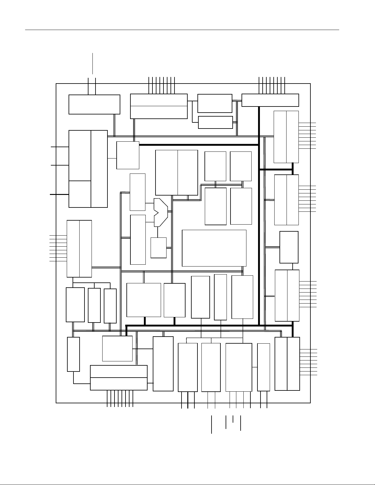
Figure 1. Block Diagram
A
MANAGEMENT
I/O
DS80C400
MDC MDIO
MII I/O (15)
OW
OWSTP
1-WIRE
CONTROLLER
MII
MII
BUFFER CONTROL UNIT
P1.0–P1.7
PORT 1
PORT LATCH
SRAM
9kk x 8
B
P0.0–P0.7
SERIAL
PORT 0
PORT 1
TIMER 2
PORT 7
PORT LATCH
STACK
MATH
ADDER
ONE’S COMP.
ACCELERATOR
POINTER
256 x 8
SFRs/ SRAM
TIMED
INTERRUPT
ACCESS
LOGIC
PORT 2
P2.0–P2.7 P7.0–P7.7
PORT LATCH
P3.0–P3.7
PORT 3
SERIAL
TIMER 3
PORT 0
PORT LATCH
TIMER 0
DATA BUS
TIMER 1
CAN
SRAM
256 x 8
PORT LATCH
PORT 5
P5.0–P5.7
ACCUMULATOR
DPTR0
DPTR1
DPTR2
PSW
DPTR3
CAN 0
CONTROLLER
COUNTER
PROGRAM
POWER
CC
MONITOR
V
(1)
(4)
(4)
SS
CC1
CC3
V
V
V
OSCILLATOR-
FAIL DETECT
ROM
BOOT
64k x 8
WATCHDOG
RESET
CONTROL
RST
RSTOL
REGISTER
INTRUCTION
MEMORY
CONTROL
CLOCK AND
EA
MUX
PSEN
DDRESS BUS
PORT LATCH
PORT LATCH
OSCILLATOR
ALE
XTAL1
XTAL2
SERIAL
PORT 2
PORT 6
PORT 4
P6.0–P6.7
P4.0– 4.7
3 of 125
 Loading...