dallas semiconductor DS5002FP service manual
CE2
PE2
W
PE3
PE4
C
C
PF V
G
P
C
C
N
BD4
查询DS5002FMN-16供应商
www.maxim-ic.com
DS5002FP
Secure Microprocessor Chip
GENERAL DESCRIPTION
The DS5002FP secure microprocessor chip is a
secure version of the DS5001FP 128k soft
microprocessor chip. In addition to the memory and
I/O enhancements of the DS5001FP, the secure
microprocessor chip incorporates the most
sophisticated security features available in any
processor. The security features of the DS5002FP
include an array of mechanisms that are designed to
resist all levels of threat, including observation,
analysis, and physical attack. As a result, a massive
effort is required to obtain any information about
memory contents. Furthermore, the “soft” nature of
the DS5002FP allows frequent modification of the
secure information, thereby minimizing the value of
any secure information obtained by such a massive
effort.
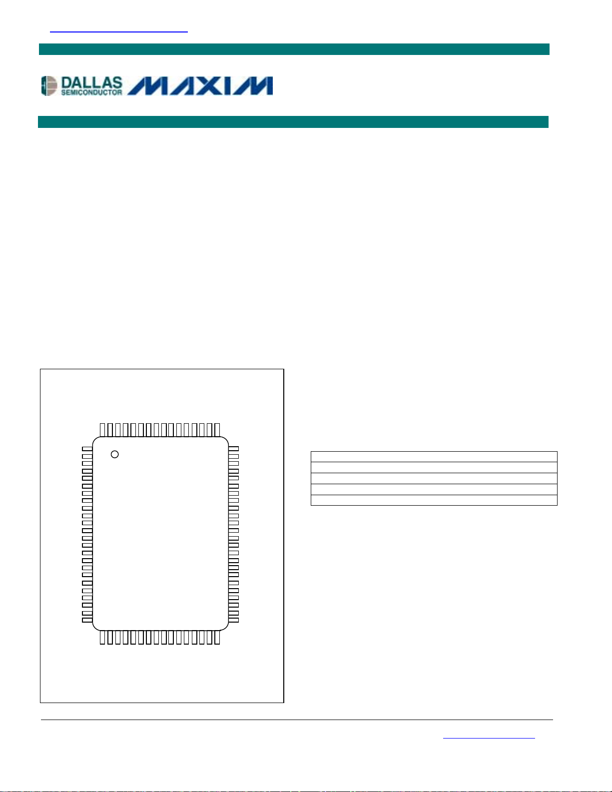
PIN CONFIGURATION
TOP VIEW
E1
P0.7/AD7
N.C.
Dallas
E1
BD7
ALE
BD6
N.C.
BD5
P2.7/A15
P2.6/A14
64
63
E3
62
E4
61
BD3
60
P2.5/A13
59
BD2
58
P2.4/A12
57
BD1
56
P2.3/A11
55
BD0
54
VLI
53
SDI
52
GND
51
P2.2/A10
50
P2.1/A9
49
P2.0/A8
48
XTAL1
47
XTAL2
46
P3.7/RD
45
P3.6/WR
44
P3.5/TI
43
42
RST
41
P3.4/T0
P0.3/AD3
P0.2/AD2
P0.1/AD1
P0.0/AD0
P0.4AD4
BA9
BA8
BA13
R/
V
V
MSEL
P1.0
BA14
P1.1
BA12
P1.2
BA7
P1.3
BA6
E1
BA11
P0.5/AD5
P0.6/AD6
BA10
80 79 78 77 76 75 74 73 72 71 70 69 68 67 66 65
1
2
3
4
5
6
7
8
Semiconductor
9
10
11
12
CC0
13
CC
14
15
16
17
18
19
20
21
22
23
24
25 26 27 28 29 30 31 32 33 34 35 36 37 38 39 40
DS5002FP
FEATURES
§ 8051-Compatible Microprocessor for
Secure/Sensitive Applications
Access 32kB, 64kB, or 128kB of NV SRAM for
Program and/or Data Storage
In-System Programming Through On-Chip Serial
Port
Can Modify Its Own Program or Data Memory in
the End System
§ Firmware Security Features
Memory Stored in Encrypted Form
Encryption Using On-Chip 64-Bit Key
Automatic True Random Key Generator
Self Destruct Input (SDI)
Optional Top Coating Prevents Microprobe
(DS5002FPM)
Improved Security Over Previous Generations
Protects Memory Contents from Piracy
§ Crash-Proof Operation
Maintains All Nonvolatile Resources for Over 10
Years in the Absence of Power
Power-Fail Reset
Early Warning Power-Fail Interrupt
Watchdog Timer
ORDERING INFORMATION
PART TEMP RANGE PIN-PACKAGE
DS5002FP-16 0°C to +70°C 80 QFP
DS5002FPM-16 0°C to +70°C 80 QFP
DS5002FP-16N -40°C to +85°C 80 QFP
DS5002FMN-16 -40°C to +85°C 80 QFP
Selector Guide appears at end of data sheet.
BA5
BA4
BA3
BA2
BA1
BA0
P1.4
P1.5
P1.6
P1.7
PRO
RST
P3.1/TXD
P3.0/RXD
P3.2/INT0
P3.3/INT1
QFP
Note: Some revisions of this device may incorporate deviations from published specifications known as errata. Multiple revisions of any device
may be simultaneously available through various sales channels. For information about device errata, click here: www.maxim-ic.com/errata
1 of 25
REV: 030503
.

DS5002FP Secure Microprocessor Chip
ELECTRICAL SPECIFICATIONS
The DS5002FP adheres to all AC and DC electrical specifications published for the DS5001FP. The absolute
maximum ratings and unique specifications for the DS5002FP are listed below.
ABSOLUTE MAXIMUM RATINGS
Voltage Range on Any Pin Relative to Ground -0.3V to (VCC + 0.5V)
Voltage Range on V
Relative to Ground -0.3V to +6.0V
CC
Operating Temperature Range -40°C to +85°C
Storage Temperature* -55°C to +125°C
Soldering Temperature See IPC/JEDEC J-STD-020A
This is a stress rating only and functional operation of the device at these or any other conditions beyond those indicated in the operation
sections of this specification is not implied. Exposure to absolute maximum rating conditions for extended periods of time can affect reliability.
*Storage temperature is defined as the temperature of the device when VCC = 0V and VLI = 0V. In this state the contents of SRAM are not
battery-backed and are undefined.
DC CHARACTERISTICS
(VCC = 5V ±10%, TA = 0°C to +70°C.)
PARAMETER SYMBOL CONDITIONS MIN TYP MAX UNITS
Input Low Voltage VIL (Note 1) -0.3 +0.8 V
+
V
Input High Voltage V
Input High Voltage
(RST, XTAL1,
PROG)
Output Low Voltage at IOL = 1.6mA
(Ports 1, 2, 3,
PF)
Output Low Voltage at IOL = 3.2mA
(Ports 0, ALE, BA15–0, BD7–0, R/
CE1N, CE 1–4, PE 1–4, V
RST
W,
)
Output High Voltage at IOH = -80µA
(Ports 1, 2, 3)
Output High Voltage at IOH = -400µA
(Ports 0, ALE, BA15–0, BD7–0, R/
CE1N, CE 1–4, PE 1–4, V
RST
W,
)
Input Low Current
V
= 0.45V (Ports 1, 2, 3)
IN
Transition Current; 1 to 0
V
= 2.0V (Ports 1, 2, 3)
IN
SDI Input Low Voltage V
SDI Input High Voltage V
SDI Pulldown Resistor R
(Note 1) 2.0
IH1
V
(Note 1) 3.5
IH2
V
(Notes 1, 13) 0.15 0.45 V
OL1
(Note 1) 0.15 0.45 V
V
OL2
V
(Note 1) 2.4 4.8 V
OH1
(Note 1) 2.4 4.8 V
V
OH2
-50 µA
I
IL
0°C to +70°C -500
I
TL
I
TL
ILS
IHS
SDI
-40°C to +85°C
(Note 12)
-600
(Note 1) 0.4 V
(Notes 1, 11) 2.0 V
25 60 k!
CC
0.3
+
V
CC
0.3
V
CCO
V
V
µA
µA
2 of 25

DS5002FP Secure Microprocessor Chip
DC CHARACTERISTICS (continued)
(VCC = 5V ±10%, TA = 0°C to +70°C.)
PARAMETER SYMBOL CONDITIONS MIN TYP MAX UNITS
Input Leakage Current (Port 0,
MSEL)
RST Pulldown Resistor RRE
VRST Pullup Resistor
PROG Pullup Resistor
Power-Fail Warning Voltage V
Minimum Operating Voltage V
I
0.45 < VIN < VCC +10 µA
IL
0°C to +70°C 40 150
-40°C to +85°C (Note 12) 30 180
R
4.7 k!
VR
40 k!
R
PR
0°C to +70°C (Note 1) 4.25 4.37 4.5
PFW
CCMIN
-40°C to +85°C (Notes 1, 12) 4.1 4.37 4.6
0°C to +70°C (Note 1) 4.00 4.12 4.25
-40°C to +85°C (Notes 1, 12) 3.85 4.09 4.25
k!
V
V
Lithium Supply Voltage VLI (Note 1) 2.5 4.0 V
Operating Current at 16MHz ICC (Note 2) 36 mA
Idle Mode Current at 12MHz I
Stop Mode Current I
IDLE
STOP
0°C to +70°C (Note 3) 7.0
-40°C to +85°C (Notes 3, 12) 8.0
mA
(Note 4) 80 µA
Pin Capacitance CIN (Note 5) 10 pF
Output Supply Voltage (V
Output Supply Battery-Backed
Mode (V
, CE1–4, PE 1–2)
CCO
Output Supply Current (Note 6) I
) V
CCO
V
CCO1
CCO1
CCO2
Current (Note 7)
Reset Trip Point in Stop Mode
(Notes 1, 2)
0°C to +70°C (Notes 1, 8)
-40°C to +85°C (Notes 1, 8,
12)
V
I
LI
= VCC - 0.45V 75 mA
CCO
0°C to +70°C 5 75 Lithium-Backed Quiescent
-40°C to +85°C 75 500
BAT = 3.0V (0°C to +70°C)
(Note 1)
BAT = 3.0V (-40°C to +85°C)
(Notes 1, 12)
BAT = 3.3V (0°C to +70°C)
(Note 1)
CC
-0.45
V
LI
-0.65
V
LI
-0.9
4.0 4.25
3.85 4.25
4.4 4.65
V
V
nA
V
AC CHARACTERISTICS
(VCC = 0V to 5V, TA = 0°C to +70°C.)
PARAMETER SYMBOL CONDITIONS MIN TYP MAX UNITS
SDI Pulse Reject (Note 10) t
SDI Pulse Accept (Note 10) t
SPR
SPA
4.5V < VCC < 5.5V 2
V
= 0V, V
CC
4.5V < VCC < 5.5V 10
V
CC
= 0V, V
= 2.9V 4
BAT
= 2.9V 50
BAT
µs
µs
3 of 25
DS5002FP Secure Microprocessor Chip
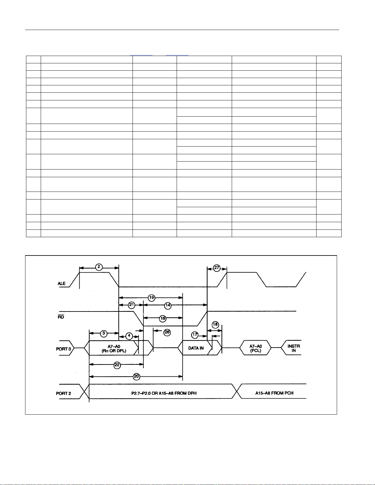
AC CHARACTERISTICS—EXPANDED BUS MODE TIMING SPECIFICATIONS
(VCC = 5V ±10%, TA = 0°C to +70°C.) (Figure 1 and Figure 2)
# PARAMETER SYMBOL CONDITIONS MIN MAX UNITS
1 Oscillator Frequency 1 / t
2 ALE Pulse Width t
3 Address Valid to ALE Low t
4 Address Hold After ALE Low t
14
RD Pulse Width
15
WR Pulse Width
16
RD Low to Valid Data In
17
Data Hold after
18
Data Float after
RD High
RD High
19 ALE Low to Valid Data In t
20 Valid Address to Valid Data In t
21
ALE Low to
Address Valid to
22
Low
23
Data Valid to
24
Data Valid to
25
Data Valid after
26
RD Low to Address Float
27
RD or WR High to ALE High
RD or WR Low
RD or WR
WR Going Low
WR High
WR High
Figure 1. Expanded Data Memory Read Cycle
1.0 16 MHz
CLK
2t
ALPW
t
AVALL
t
AVAAV
6t
t
RDPW
6t
t
WRPW
t
RDLDV
t
RDHDV
t
RDHDZ
ALLVD
AVDV
t
ALLRDL
t
AVRDL
t
DVWRL
t
DVWRH
t
WRHDV
t
RDLAZ
t
RDHALH
12MHz 5t
16MHz 5t
0 ns
2t
12MHz 8t
16MHz 8t
12MHz 9t
16MHz 9t
3t
4t
t
12MHz 7t
16MHz 7t
t
0 ns
t
- 40 ns
CLK
- 40 ns
CLK
- 35 ns
CLK
- 100 ns
CLK
- 100 ns
CLK
- 165
CLK
- 105
CLK
- 70 ns
CLK
- 150
CLK
- 90
CLK
- 165
CLK
- 105
CLK
- 50 3t
CLK
- 130 ns
CLK
- 60 ns
CLK
- 150
CLK
- 90
CLK
-50 ns
CLK
- 40 t
CLK
+ 50 ns
CLK
+ 50 ns
CLK
ns
ns
ns
ns
4 of 25
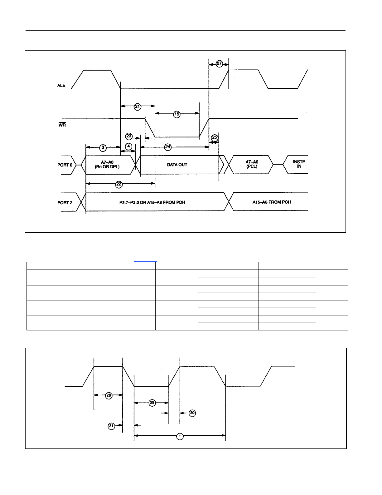
Figure 2. Expanded Data Memory Write Cycle
DS5002FP Secure Microprocessor Chip
AC CHARACTERISTICS—EXTERNAL CLOCK DRIVE
(VCC = 5V ± 10%, TA = 0°C to +70°C.) (Figure 3)
# PARAMETER SYMBOL CONDITIONS MIN MAX UNITS
28 External Clock High Time t
29 External Clock Low Time t
30 External Clock Rise Time t
31 External Clock Fall Time t
Figure 3. External Clock Timing
CLKHPW
CLKLPW
CLKR
CLKF
12MHz 20
16MHz 15
12MHz 20
16MHz 15
12MHz 20
16MHz 15
12MHz 20
16MHz 15
ns
ns
ns
ns
5 of 25
DS5002FP Secure Microprocessor Chip
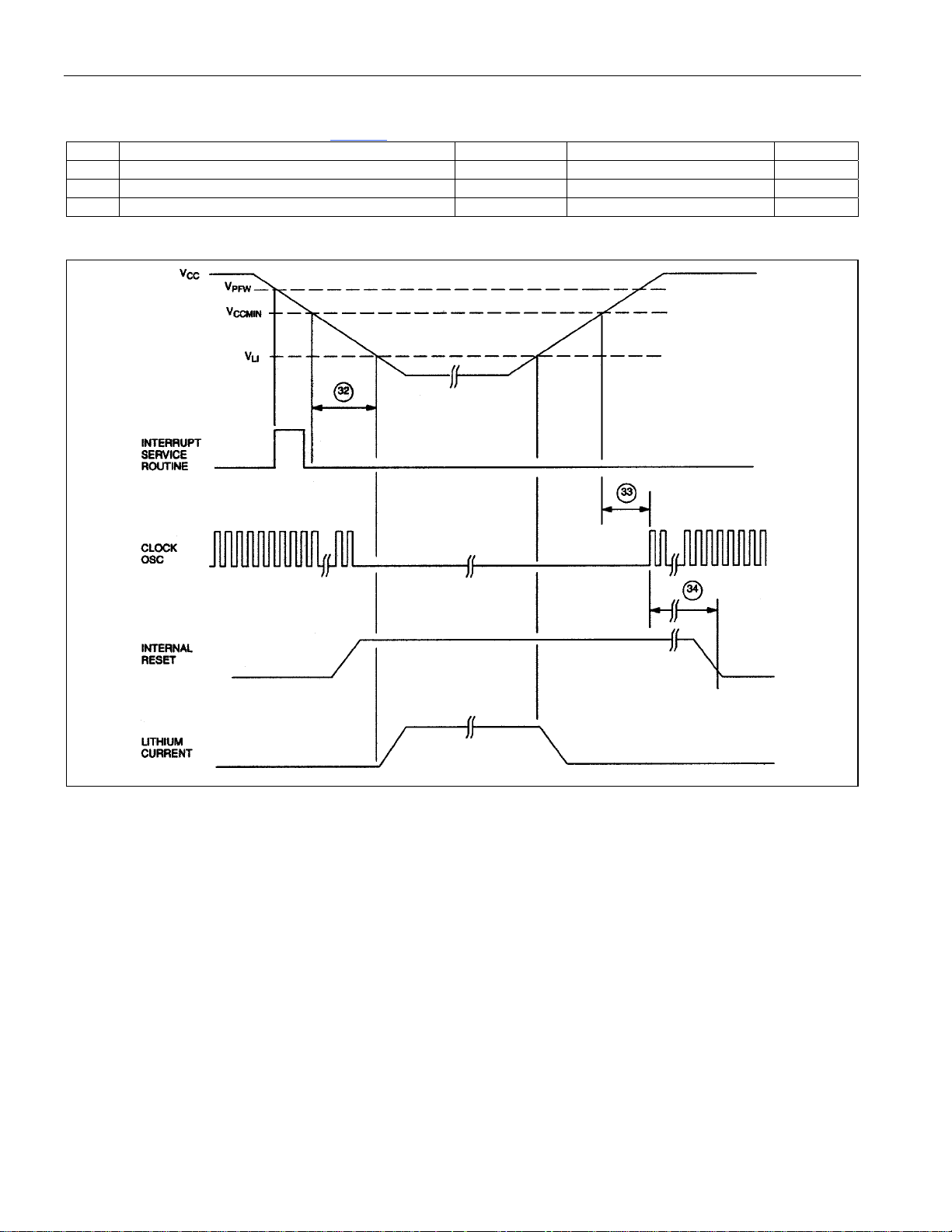
AC CHARACTERISTICS—POWER CYCLE TIME
(VCC = 5V ±10%, TA = 0°C to +70°C.) (Figure 4)
# PARAMETER SYMBOL MIN MAX UNITS
32 Slew Rate from V
33 Crystal Startup Time t
34 Power-on Reset Delay t
Figure 4. Power Cycle Timing
to VLI t
CCMIN
130 µs
F
(Note 9)
CSU
21504 t
POR
CLK
6 of 25
DS5002FP Secure Microprocessor Chip
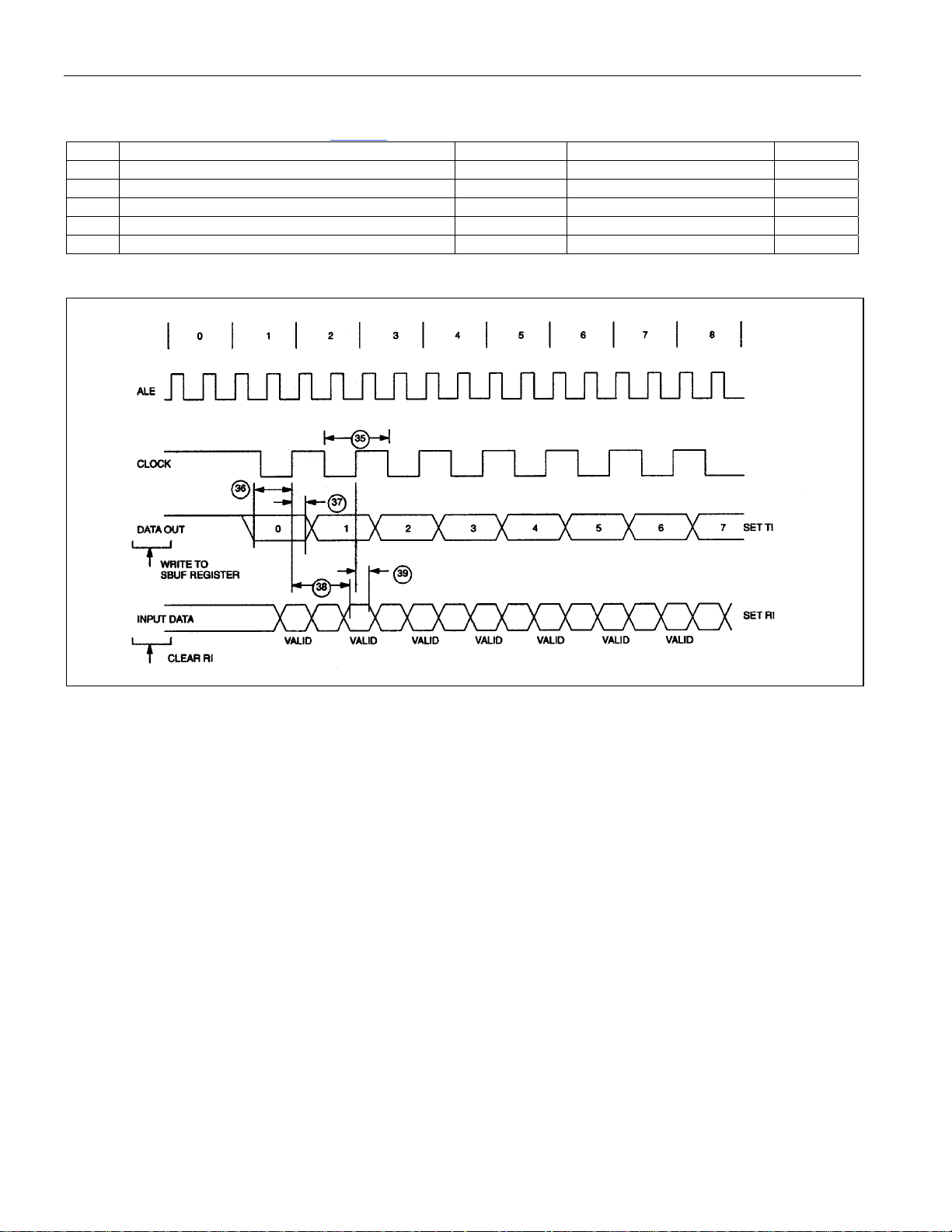
AC CHARACTERISTICS—SERIAL PORT TIMING, MODE 0
(VCC = 5V ±10%, TA = 0°C to +70°C.) (Figure 5)
# PARAMETER SYMBOL MIN MAX UNITS
35 Serial Port Clock Cycle Time t
36 Output Data Setup to Rising Clock Edge t
37 Output Data Hold after Rising Clock Edge t
38 Clock Rising Edge to Input Data Valid t
39 Input Data Hold after Rising Clock Edge t
Figure 5. Serial Port Timing, Mode 0
12t
SPCLK
10t
DOCH
2t
CHDO
10t
CHDV
0 ns
CHDIV
µs
CLK
- 133 ns
CLK
- 117 ns
CLK
- 133 ns
CLK
7 of 25
DS5002FP Secure Microprocessor Chip
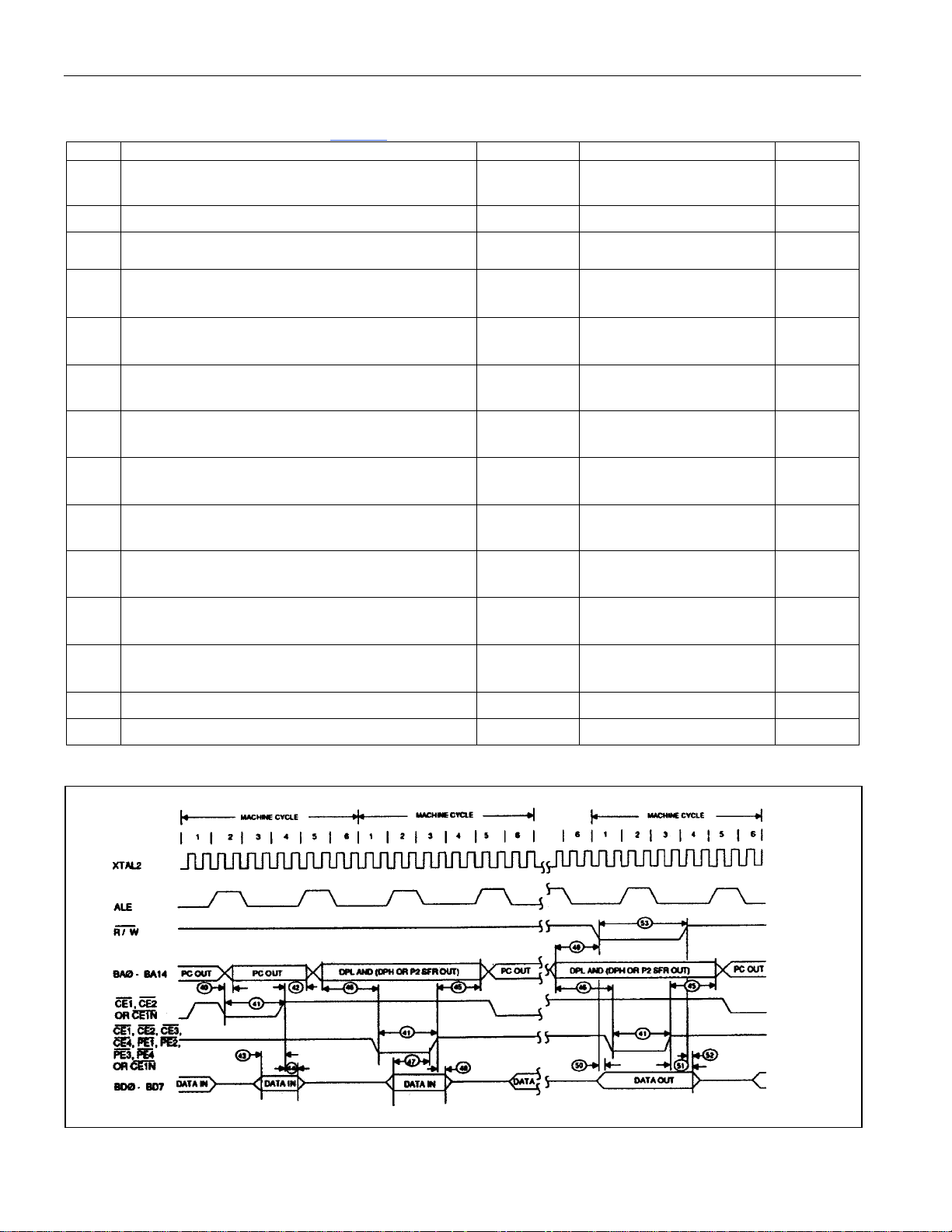
AC CHARACTERISTICS—BYTE-WIDE ADDRESS/DATA BUS TIMING
(VCC = 5V ±10%, TA = 0°C to +70°C.) (Figure 6)
# PARAMETER SYMBOL MIN MAX UNITS
Delay to Byte-Wide Address Valid from
40
CE2, or CE1N Low During Op Code Fetch
41
Pulse Width of
Byte-Wide Address Hold After
42
CE1N High During Op Code Fetch
Byte-Wide Data Setup to
43
High During Op Code Fetch
CE1–4, PE1–4, or CE1N
CE1, CE2, or CE1N
CE1, CE2, or
CE1,
30 ns
t
CE1LPA
t
CEPW
t
CE1HPA
t
OVCE1H
4t
2t
1t
- 35 ns
CLK
- 20 ns
CLK
+ 40 ns
CLK
Byte-Wide Data Hold After
44
High During Op Code Fetch
Byte-Wide Address Hold After
45
CE1N High During MOVX
Delay from Byte-Wide Address Valid
46
PE1–4, or CE1N Low During MOVX
Byte-Wide Data Setup to
47
CE1N High During MOVX (Read)
Byte-Wide Data Hold After
48
CE1N High During MOVX (Read)
Byte-Wide Address Valid to R/
49
MOVX (Write)
Delay from R/
50
MOVX (Write)
Valid Data Out Hold Time from
51
CE1N High
52
Valid Data Out Hold Time from R/
53
Write Pulse Width (R/
W Low to Valid Data Out During
CE1, CE2, or CE1N
CE1–4, PE1–4, or
CE1–4, PE1–4, or
W Active During
W Low Time)
Figure 6. Byte-Wide Bus Timing
CE1–4, PE1–4, or
CE1–4,
CE1–4, PE1–4, or
W High
0 ns
t
CE1HOV
4t
t
CEHDA
4t
t
CELDA
1t
t
DACEH
0 ns
t
CEHDV
t
3t
AVRWL
20 ns
t
RWLDV
1t
t
CEHDV
0 ns
t
RWHDV
t
6t
RWLPW
- 30 ns
CLK
- 35 ns
CLK
+ 40 ns
CLK
- 35 ns
CLK
- 15 ns
CLK
- 20 ns
CLK
8 of 25
 Loading...