dallas semiconductor DS4812 service manual

查询DS3881供应商
www.dalsemi.com
PRELIMINARY
DS4812
Low Voltage, High Slew Rate,
Rail-To-Rail Dual Op-Amp
FEATURES
High Slew Rate: 10V/µs
High Gain Bandwidth: 6.5 MHz
Supply Voltage Range 2.5 to 5.5V
Rail-to-Rail Output Swing
1.75 mA Supply Current per Channel
ORDERING INFORMATION
Part Number Description
DS4812 8-pin DIP
DS4812S 8-pin SOIC
DS4812U
DS4812X 8-bump CSP
For mechanical dimensions see web site.
8-pin µ-SOP
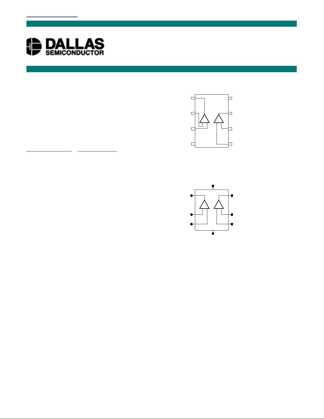
PACKAGES/PINOUTS
1
AOUT
2
AIN-
A
-
+
3
AIN+
45
GND
300-mil DIP
150-mil SOIC
118-mil µ-SOP
VDD
1
AOUT
A
-
+
2
AIN-
3
AIN+
GND
8
VDD
7
BOUT
B
-
+
6
BIN-
BIN+
8
7
BOUT
B
-
+
6
BIN-
5
BIN+
4
8-bump CSP
DESCRIPTION
The DS4812 BiCMOS dual operational amplifier combines high slew rate and rail-to-rail output swing.
The device provides 10V/µs of slew rate and 6.5 MHz of bandwidth while only consuming 1.5 mA of
supply current per channel. Ideal low voltage BiFET substitute for low gain, high speed applications.
1 of 19 101000

ABSOLUTE MAXIMUM RATINGS
Supply Voltage, VDD (see Note 1)............5.5V
DS4812
Differential Input Voltage (see Note 2)....± V
Input Voltage Range, VI(see Note 1) .......-0.3V to V
DD
DD
Input Current, IDD.....................................± 4 mA
Output Current, IO....................................± 50 mA
Total current into VDD..............................± 50 mA
Total current out of GND.........................± 50 mA
Duration of short-circuit current (See Note 3) unlimited
Operating Temperature............................0 oC to +70 oC
Storage Temperature................................-55 oC to +125 oC
Soldering Temperature.............................See J-STD-020A Specification
NOTES:
1. Relative to GND.
2. Non-inverting input relative to inverting input. Excessive current flows when input is brought below
GND - 0.3V.
3. The output may be shorted to either supply. Temperature and/or supply voltages must be limited to
ensure that the maximum dissipation rating is not exceeded.
RECOMMENDED OPERATING CONDITIONS
PARAMETER SYMBOL MIN TYP MAX UNITS NOTES
Supply Voltage V
Input Voltage Range V
Common-Mode Input Voltage V
Free-Air Operating Temperature T
DD
I
CM
A
2.5 5.5 V 1
0V
0V
070
- 1.7 V 1
DD
- 1.7 V
DD
o
C
NOTES:
1. Voltage referenced to GND.
2 of 19

ELECTRICAL CHARACTERISTICS
DS4812
Conditions: (T
: 0°C – 70°C. VDD = 3.0V)
A
PARAMETER SYMBOL MIN TYP MAX UNITS NOTES
Input Offset Voltage
= 0.5V, RS = 50Ω, V
(V
IC
OUT
= 1.5V)
V
IO
15mV
Temperature Coefficient of Input Offset
Voltage
(V
= 0.5V, RS = 50Ω, V
IC
OUT
= 1.5V)
Input Offset Current
(V
= 0.5V, RS = 50Ω, V
IC
OUT
= 1.5V)
Input Bias Current
(V
= 0.5V, RS = 50Ω, V
IC
OUT
= 1.5V)
Common-mode Input Voltage Range
| ≤ 10mV
|V
IO
High Level Output Voltage
(IOH = -0.5 mA)
Low Level Output Voltage
(IOL = 0.5 mA)
αV
I
I
V
V
V
IO
IB
ICR
OH
OL
IO
0 1.3 V
2.5 2.8 V
10
µV/°C
1 500 pA
2 500 pA
0.15 0.5 V
Large Signal Differential Voltage
Amplification
(V
= 0.5V, RL = 10 kΩ, 1V ≤ VO ≤ 2V)
IC
Common Mode Input Capacitance c
Common Mode Rejection Ratio
(0V ≤ V
≤ 1.0V, VO = 1.5V)
IC
A
VD
i(c)
60 68 dB
4pF
CMRR 40 50 dB
Supply Voltage Rejection Ratio
(3V ≤ V
DD
≤ 5V, V
= VDD/2 – 1V, no
IC
k
SVR
70 80 dB
load)
Amplifier Supply Current (per channel)
(VO = 1.5V, no load)
Slew Rate at Unity Gain
= 50 pF)
(C
L
Unity Gain Bandwidth
(CL = 50 pF)
Phase Margin at Unity Gain
= 50 pF)
(C
L
Gain Margin
(CL = 50 pF)
I
DD
SR 5 7.5
1.5 2.5 mA
V/µs
UGBW 5.0 MHz
φ
M
54 Degree
6dB
3 of 19

ELECTRICAL CHARACTERISTICS cont.
DS4812
Conditions: (T
: 0°C – 70°C. VDD = 5.0V)
A
PARAMETER SYMBOL MIN TYP MAX UNITS NOTES
Input Offset Voltage
= 1.5V, RS = 50Ω, V
(V
IC
OUT
= 2.5V)
V
IO
15mV
Temperature Coefficient of Input Offset
Voltage
(V
= 1.5V, RS = 50Ω, V
IC
OUT
= 2.5V)
Input Offset Current
(V
= 1.5V, RS = 50Ω, V
IC
OUT
= 2.5V)
Input Bias Current
(V
= 1.5V, RS = 50Ω, V
IC
OUT
= 2.5V)
Common-mode Input Voltage Range
| ≤ 10 mV
|V
IO
High Level Output Voltage
(IOH = -1.0 mA)
Low Level Output Voltage
(IOL = 1.0 mA)
αV
I
I
V
V
V
IO
IB
ICR
OH
OL
IO
0 3.3 V
4.5 4.8 V
10
µV/°C
1 500 pA
2 500 pA
0.15 0.5 V
Large Signal Differential Voltage
Amplification
(V
= 1.5V, RL = 10 kΩ, 1.5V ≤ VO ≤ 3.5V)
IC
Common Mode Input Capacitance c
Common Mode Rejection Ratio
(0V ≤ V
≤ 2.7V, VO = 2.5V)
IC
Supply Voltage Rejection Ratio
(3V ≤ V
DD
≤ 5V, V
= VDD/2 – 1V, no load)
IC
Amplifier Supply Current (per channel)
(VO = 2.5V, no load)
Slew Rate at Unity Gain
(CL = 50 pF)
Unity Gain Bandwidth
(C
= 50 pF)
L
Phase Margin at Unity Gain
(C
= 50 pF)
L
Gain Margin
= 50 pF)
(C
L
A
VD
i(c)
60 72 dB
4pF
CMRR 45 55 dB
k
SVR
I
DD
SR 7 10
70 80 dB
1.75 2.5 mA
V/µs
UGBW 6.5 MHz
φ
M
46 Degree
4dB
4 of 19

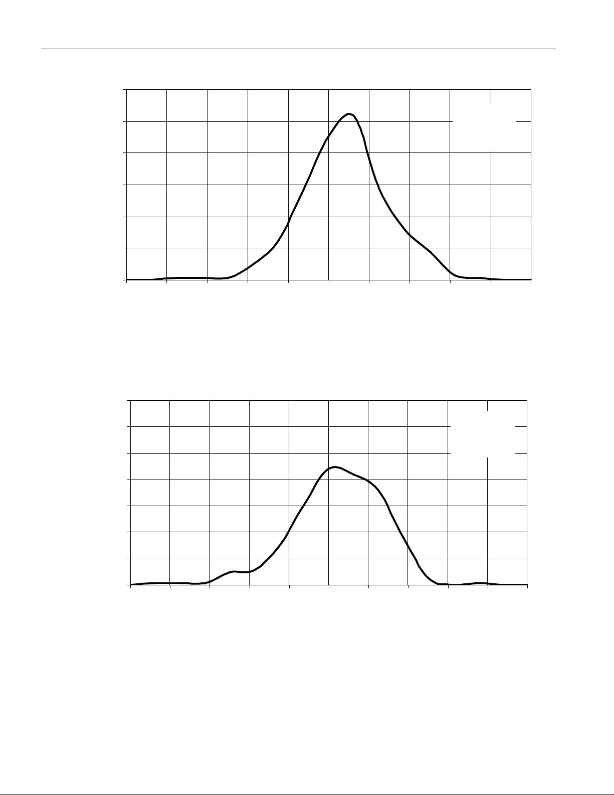
DISTRI BUTIO N OF DS481 2
INPUT OFFSET VOLTAG E
30%
VDD = 3.0 V
25%
= 10K
R
L
T
= 25oC
A
20%
15%
10%
5%
Percentage of Amplifiers - %
0%
-2.0 -1.6 -1.2 -0.8 -0.4 0.0 0.4 0.8 1.2 1.6 2.0
V
- I nput O f f set Voltage - m V
IO
Figure 1.0
DS4812
Percentage of Amplifiers - %
DISTRI BUTI ON O F DS481 2
INPUT OFFSET VOLTAGE
35%
30%
25%
VDD = 5. 0 V
R
= 10K
L
T
= 25oC
A
20%
15%
10%
5%
0%
-2 -1.6 -1.2 -0.8 -0.4 0 0.4 0.8 1.2 1.6 2
V
- Input Off set Vol t age - m V
IO
Figure 2.0
5 of 19

DS4812
V
V
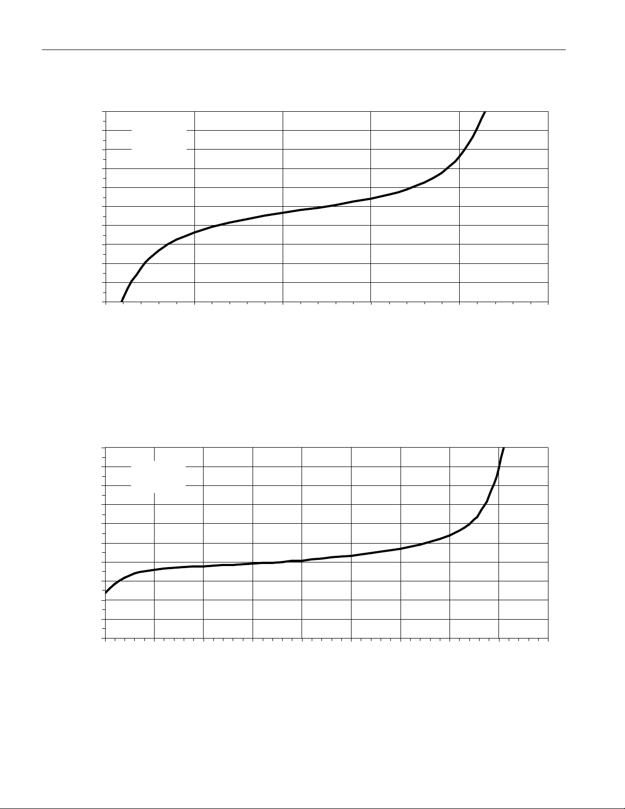
INPUT O FF SET VO L TAG E
vs
COMM ON- MODE I N PUT V OLTAGE
5
4
3
VDD = 3. 0 V
T
= 25oC
A
2
1
0
-1
-2
-3
- Input Offset Voltage - m
IO
V
-4
-5
-0.5 0 0.5 1 1.5 2
V
- Common-Mode Input Voltage - V
IC
Figure 3.0
INPUT O FF SET VO L TAG E
vs
COMMON-MODE INPUT VOLTAGE
5
4
3
VDD = 5. 0 V
= 25oC
T
A
2
1
0
-1
-2
- Input Offset Voltage - m
-3
IO
V
-4
-5
-0.500.511.522.533.54
V
- Common-Mode Input Voltage - V
IC
Figure 4.0
6 of 19
 Loading...