Dallas Semiconductor DS2890P-T-R, DS2890P, DS2890-T-R, DS2890, DS2890X Datasheet
1 of 27 061500
FEATURES
Single element 256-position linear taper
potentiometer
Supports potentiometer terminal working
voltages up to 11V
Potentiometer terminal voltage independent
of supply voltage
Potentiometer wiper position controlled and
read over minimal 1-Wire bus interface
100 kΩ resistor element value
Provides 1-Wire and VDD power modes
Supports Conditional Search based on
power-on default wiper position
Multiple DS2890’s can be identified on a
common 1-Wire bus and operated
independently
Unique factory lasered 64-bit registration
number assures error free device selection
and absolute part identity
Built-in multi-drop controller ensures
compatibility with other 1-Wire Network
products
Supports Overdrive mode which boosts
communication speed up to 142 kbits per
second
-40
o
C to +85oC operating temperature range
2.8V – 6.0V operating voltage range
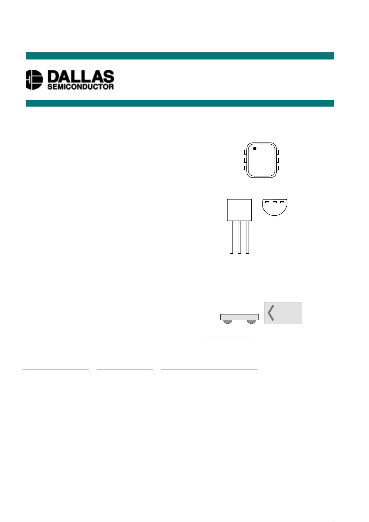
PIN ASSIGNMENT
Top View
6-pin TSOC
1-WIRE
GND
VDD
1
2
3
6
5
4
RH
WIPER
RL
TO-92 Package
123
GND
1-WIRE
RH
123
Bottom View
Flip Chip Package
side view
top view
Visit www.dalsemi.com for Flip Chip pinout and
mechanical data.
ORDERING INFORMATION
PART NUMBER RESISTANCE
*
PACKAGE DESCRIPTION
DS2890-000
100 kΩ
T0-92
DS2890P-000
100 kΩ
6-pin TSOC
DS2890X-000
100 kΩ
Flip Chip Pkg., Tape & Reel
DS2890T-000
100 kΩ
Tape & Reel of DS2890
DS2890V-000
100 kΩ
Tape & Reel of DS2890P
* Contact the factory for availability of alternate resistance values
www.dalsemi.com
PRELIMINARY
DS2890
1-Wire
®
Digital Potentiomete
r

DS2890
2 of 27
PIN DESCRIPTION
SIGNAL
NAME TYPE FUNCTION
1-WIRE I/O 1-Wire bus interface. Open drain, requires external pull-up resistor. Range:
2.8V – 6.0V. See HARDWARE CONFIGURATION for pull-up resistor
recommendations.
RH
I/O High end terminal of potentiometer resistor element. Range: 0V – 11.0V.
Range independent of 1-Wire or VDD supply levels as well as the voltage
levels applied to the other potentiometer terminals.
RL
I/O Low end terminal of potentiometer resistor element. Range: 0V – 11.0V.
Range independent of 1-Wire or V
DD
supply levels as well as the voltage
levels applied to the other potentiometer terminals.
WIPER
I/O Potentiometer wiper terminal. Range 0V – 11.0V. Range independent of
1-Wire or VDD supply levels as well as the voltage levels applied to the other
potentiometer terminals.
V
DD
PWR Auxiliary power supply input. Range: 2.8V – 6.0V
GND
PWR Ground
DESCRIPTION
The DS2890 is a linear taper digitally controlled potentiometer with 256 wiper positions. Device
operation, including wiper position, is controlled over the single contact 1-Wire bus for the ultimate in
electrical interface simplicity. With a wide 0–11 volt working voltage range for the potentiometer
terminals, the DS2890 is ideal for a broad range of industrial and control applications. Potentiometer
terminal voltage is independent of device supply voltage as well as the voltage applied to the other
potentiometer terminals. Communication with the DS2890 follows the standard Dallas Semiconductor
1-Wire protocol and can be accomplished with minimal hardware such as a single port pin of a
microcontroller. Multiple DS2890 devices can reside on a common 1-Wire bus and be operated
independently of each other. Each DS2890 has its own unalterable 64-bit ROM registration number that
is factory lasered into the chip. The registration number guarantees unique identification for absolute
traceability and is used to address the device in a multi-drop 1-Wire Network environment. The DS2890
will respond to a 1-Wire Conditional Search command if the potentiometer wiper is set at the power-on
default position. This feature enables the bus master to easily determine whether a potentiometer has
gone through a power-on reset and needs to be re-configured with a required wiper position setting. The
DS2890 supports two power modes: 1-Wire only mode in which device power is supplied parasitically
from the 1-Wire bus or VDD mode where power is supplied from an external supply; when operating from
VDD mode wiper resistance is reduced.
DS2890
3 of 27
OPERATION
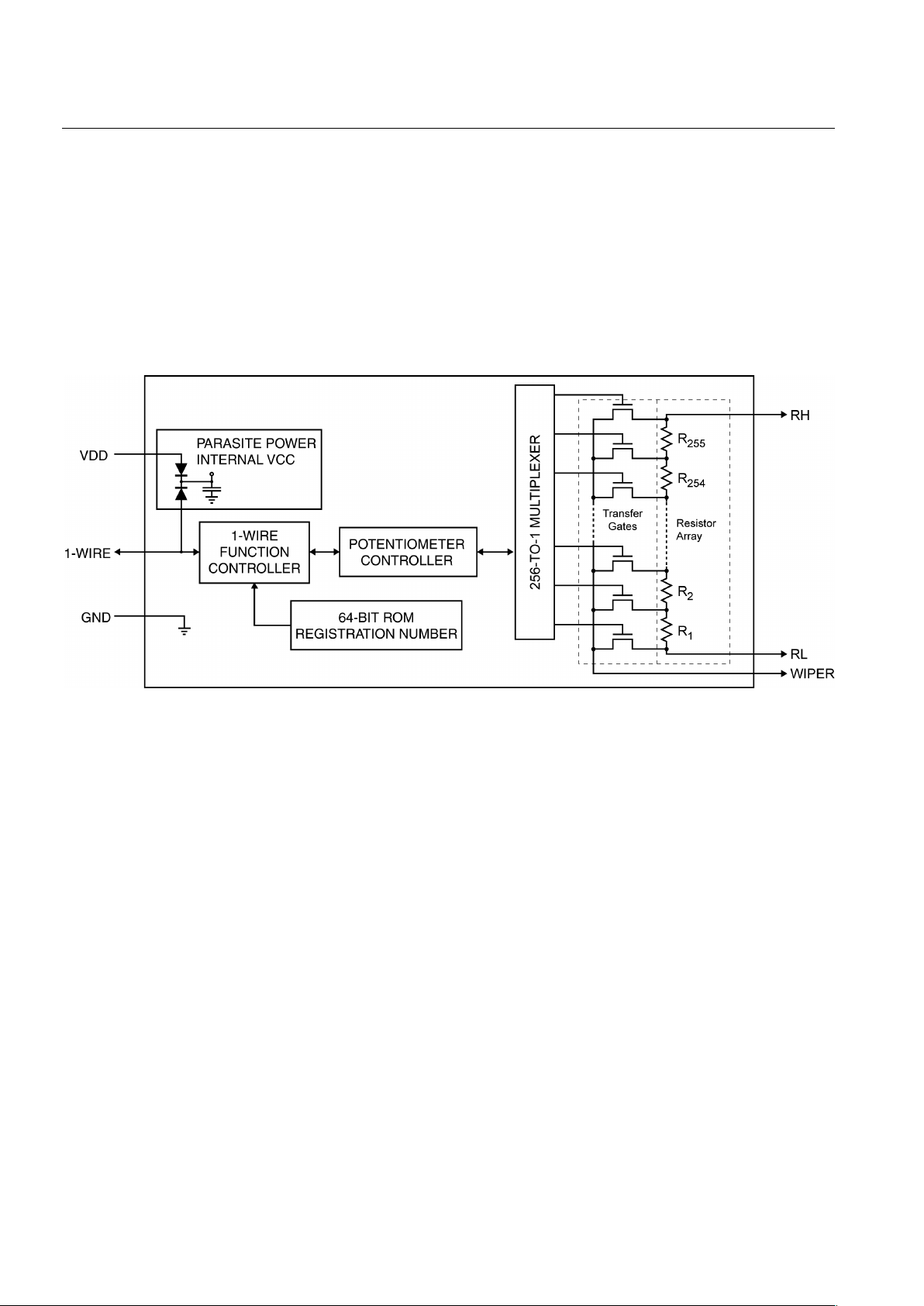
The DS2890 is a single element digital potentiometer; a block diagram of the device is shown in Figure 1.
The device has a total of 256 linearly spaced tap points including the RL and RH terminals; a total of 255
resistive segments exist between the RL and RH terminals. These tap points are ac cessible t o th e W IPER
terminal whose position is controlled via the 1-Wire bus interface. Wiper position and device state are
maintained as long as the 1-Wire bus is active or the V
DD
supply is applied within operating limits.
Otherwise, a power-on reset will occur and the wiper position and operating state will return to power-on
default conditions.
Figure 1. DS2890 BLOCK DIAGRAM
As shown in the figure the device has five major elements: the 1-Wire Function Controller, the
Potentiometer Controller, the 64-bit ROM, the resistor array, and Parasite Power circuitry. Each of these
elements is discussed in detail throughout the remainder of the data sheet. DS2890 control including
device selection, positioning/reading the potentiometer wiper, and device operating state is performed
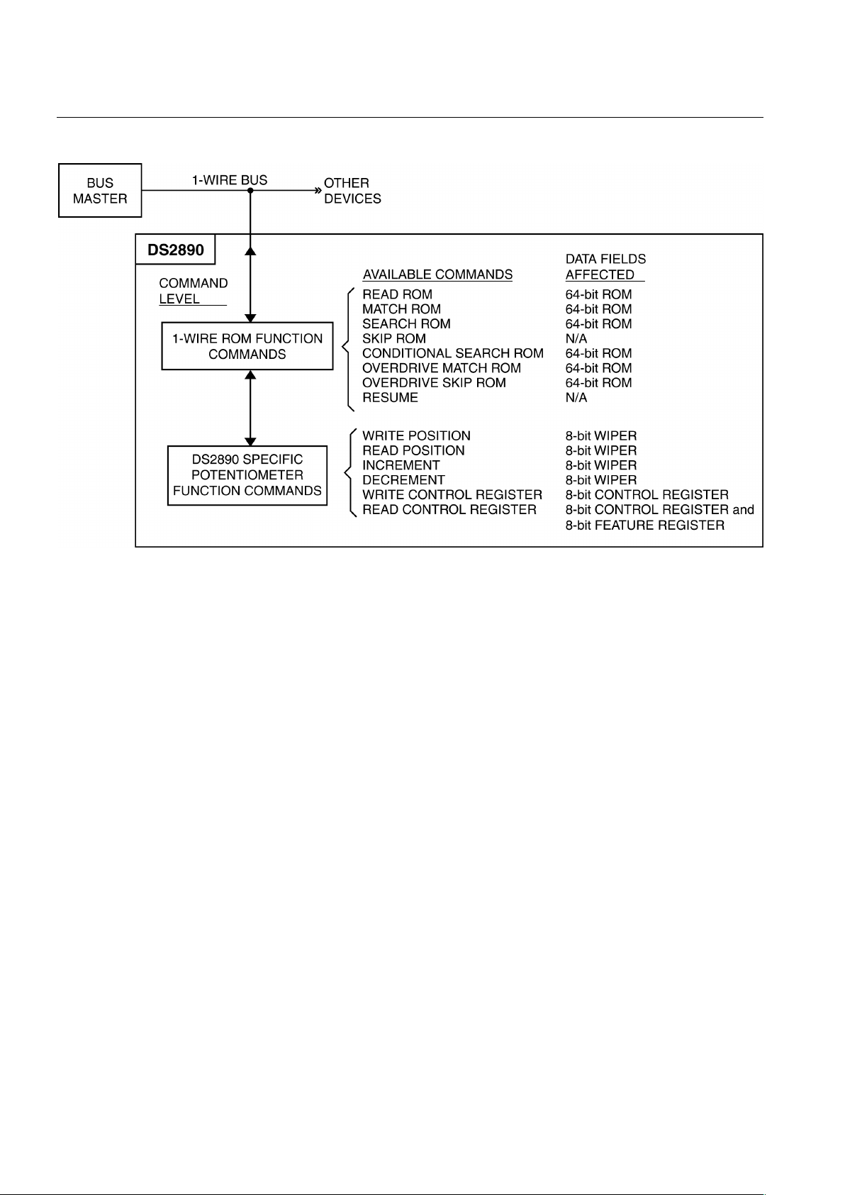
over the 1-Wire bus. The hierarchical structure of the 1-Wire protocol as applicable to the DS2890 is
shown in Figure 2. As shown, the control sequence starts with the 1-Wire bus master issuing one of eight
ROM function commands. After a ROM function command is successfully completed potentiometer
functions may be executed. The protocol for ROM and potentiometer functions are described in the
“COMMAND FLOW” section. For the 3-pin TO-92 package configuration and operation see the
“TO-92 PACKAGE OPERATION” section.
DS2890
4 of 27
Figure 2. 1-WIRE COMMAND HIERARCHICAL STRUCTURE
DATA I/O BIT ORDER
All data is read and written least significant bit (LSB) first.
POTENTIOMETER FEATURE REGISTER
Although the feature set of the DS2890 is primarily fixed, a mechanism to identify feature characteristics
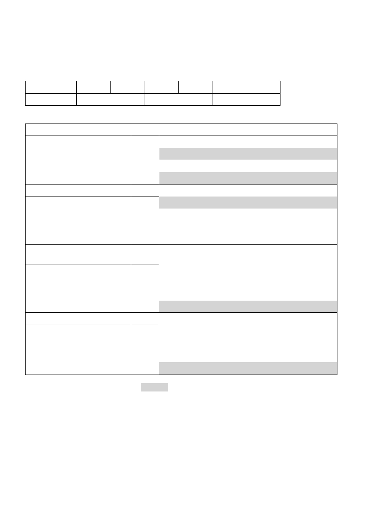
of future 1-Wire potentiometers has been developed and implemented in the DS2890. As shown in
Figure 3, the feature register is an encoded read-only byte that describes the cha ract eristics of the DS2890
and future 1-Wire potentiometers. Feature values that correspond to the DS2890 are highlighted. The
feature register is read with the READ CONTROL REGISTER potentiometer function command (see
“POTENTIOMETER FUNCTION COMMANDS”).
DS2890
5 of 27
Figure 3. 1-WIRE POTENTIOMETER FEATURE REGISTER
Feature Register Bit Encoding
b7 b6 b5 b4 b3 b2 b1 b0
PR NWP NP WSV PC
Feature Register Bit Definitions
Feature Description Bit(s) Definition
If 0: logarithmic potentiometer element(s)
PC: potentiometer characteristic b0
If 1: linear potentiometer element(s)
If 0: wiper setting(s) are non-volatile
WSV: wiper setting volatility b1
If 1: wiper setting(s) are volatile
NP: number of potentiometers b3..b2 2 bit binary value representing number of potentiometers:
If 00b: 1 potentiometer
If 01b: 2 potentiometers
If 10b: 3 potentiometers
If 11b: 4 potentiometers
NWP: number of wiper positions b5..b4
2 bit binary value representing number of wiper positions
for each potentiometer:
If 00b: 32 positions
If 01b: 64 positions
If 10b: 128 positions
If 11b: 256 positions
PR: potentiometer resistance b7..b6 2 bit binary value representing potentiometer resistance:
If 00b: 5 kΩ
If 01b: 10 kΩ
If 10b: 50 kΩ
If 11b: 100 kΩ
DS2890 feature values are highlighted: value
The DS2890 will respond with a feature register value of F3h when a READ CONTROL
REGISTER command is executed, see section “POTENTIOMETER FUNCTION COMMANDS”.
POTENTIOMETER CONTROL REGISTER
The potentiometer control register is used to turn on/off the DS2890 charge pump (see section
“POTENTIOMETER WIPER RESISTANCE AND CHARGE PUMP CONSIDERATIONS” for a
discussion of the charge pump) and has control capabilities for future 1-Wire potentiometers that could
contain multiple resistor elements. The format of the control register is shown in Figure 4.

DS2890
6 of 27
Figure 4. POTENTIOMETER CONTROL REGISTER
Control Register Bit Encoding
b7 b6 b5 b4 b3 b2 b1 b0
XCPC X X
WN
WN
Control Register Bit Definitions*
Description Bit(s) Definition
WN: wiper number to control b1..b0
2 bit binary value representing the potentiometer wiper to
control:
If 00b: potentiometer 1 wiper
If 01b: potentiometer 2 wiper
If 10b: potentiometer 3 wiper
If 11b: potentiometer 4 wiper
WN: inverted wiper number to
control
b3..b2
1’s complement of potentiometer wiper to control:
If 11b: potentiometer 1 wiper
If 10b: potentiometer 2 wiper
If 01b: potentiometer 3 wiper
If 00b: potentiometer 4 wiper
If 0: the charge pump is OFF
CPC: charge pump control b6
If 1: the charge pump is ON
X: don’t care. b4,b5,b7
These bits are reserved for future use by Dallas
Semiconductor. These bits should be written to a value of
0.
*NOTE:
Control Register power-on defaults: Charge Pump is OFF (CPC=0), Wiper Number to control is wiper #1
(WN=00b,
WN=11b).
Valid DS2890 control values are highlighted:
value
Thus for the DS2890, valid control register values are:
Control Register Value Description
00001100b charge pump off, potentiometer #1 wiper selected
01001100b charge pump on, potentiometer #1 wiper selected
As shown in Figure 17 and discussed in the “POTENTIOMETER FUNCTION COMMANDS” section,
no change in device state will occur if an invalid control register value is sent.
DS2890
7 of 27
POWER
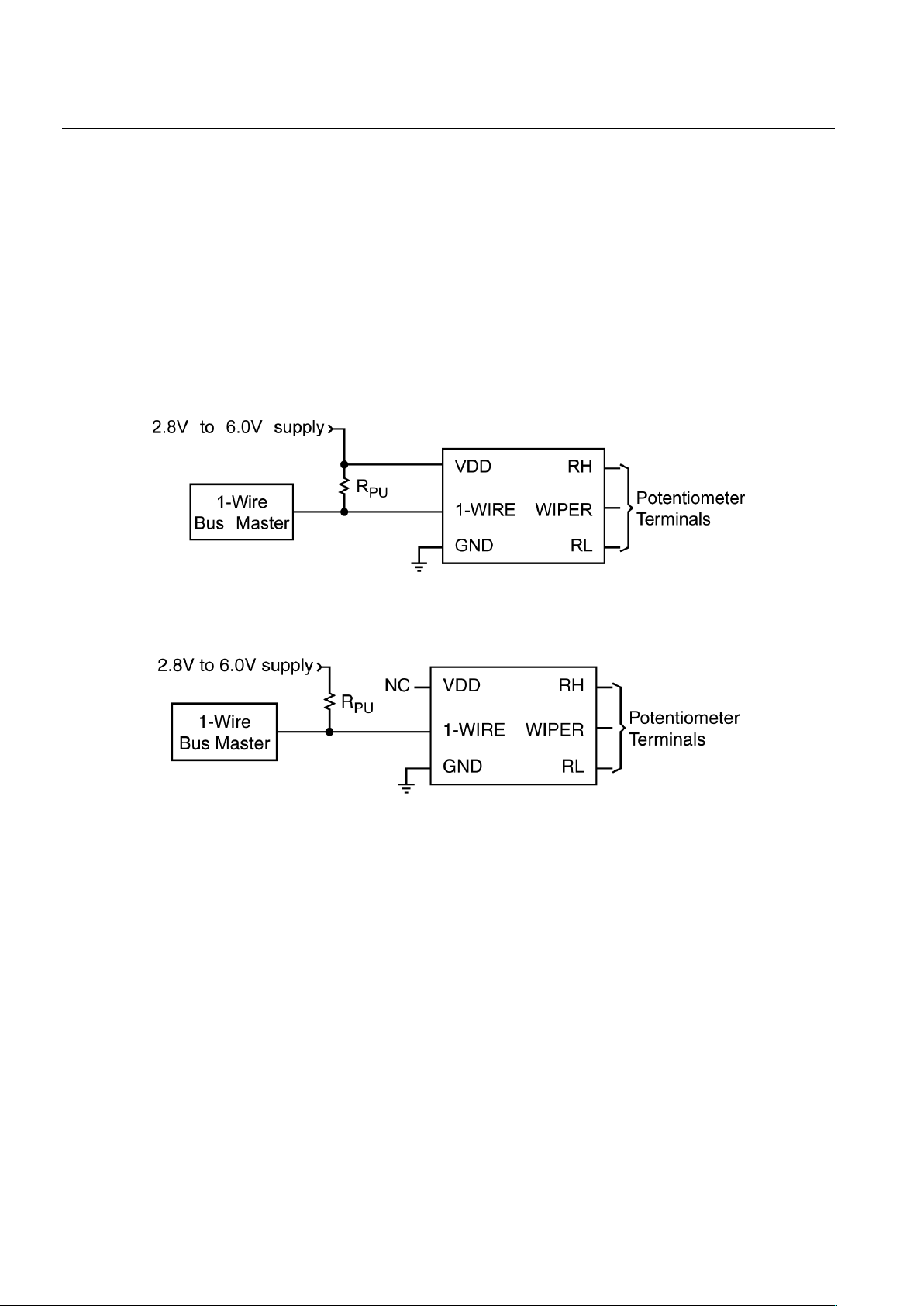
With the charge pump off, the DS2890 can derive its power entirely from the 1-Wire bus by storing
energy on an internal capacitor during periods of time when the 1-Wire bus is in a high state. During bus
low times the device continues to operate from the energy stored on the internal capacitor; the capacitor is
then recharged when the bus returns to a hi gh state. This t echniqu e of operatin g entirel y from the 1-W ire
bus by powering from energy stored on an internal capacitor during bus low times in known as “parasite
powered” operation. As an option, an auxiliary power source may be connected to the V
DD
power pin.
The auxiliary power mode is appropriate for applications where device charge pump activation is
necessary, the device may be temporarily disconnected from the 1-Wire bus, or bus low times may be
very long. See Figure 5 for example configurations for both power modes.
Figure 5. POWER SUPPLY CONFIGURATION OPTIONS
(a) Auxiliary VDD Supply Configuration
(b) 1-Wire Parasite Power Configuration
POTENTIOMETER WIPER RESISTANCE AND CHARGE PUMP
CONSIDERATIONS
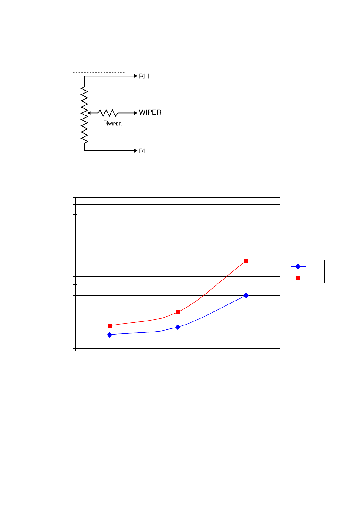
A simplified diagram of the DS2890 resistor array is shown in Figure 6. In this figure the rDS resistance
of the wiper transistors in Figure 1 are modeled as wiper resistance R
WIPER
. The value of R
WIPER
varies
with device configuration, operational state, and wiper terminal voltage. If an auxiliary external V
DD
supply configuration is used as shown In Figure 5a, the DS2890 charge pump may be enabled to reduce
potentiometer wiper resistance. A consequence of enabling the charge pump is increased device power
consumption. This increase is beyond the level that can be supported when operating in 1-Wire parasite
power mode (see POWER section). Therefore if it is necessary to enable the charge pump in an
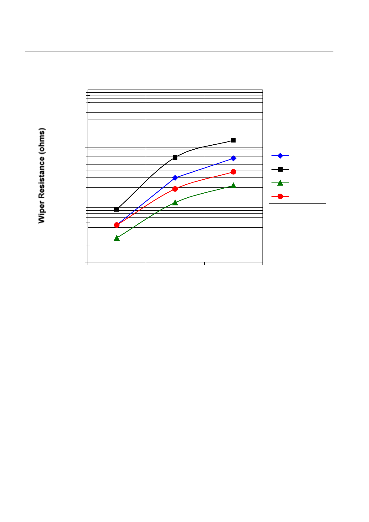
application, the power supply configuration as shown in Figure 5a must be used. Figure 7 and Figure 8
are graphs of wiper resistance with the charge pump turned ON and OFF respectively.
DS2890
8 of 27
Figure 6. POTENTIOMETER RESISTOR MODEL
Figure 7. TYPICAL WIPER RESISTANCE VS WIPER VOLTAGE,
CHARGE PUMP ON
100
1000
10000
0.1 5.5 11
Wiper Volt age ( V)
Wiper Resistance (ohms)
25C
85C
DS2890
9 of 27
Figure 8. TYPICAL WIPER RESISTANCE VS WIPER VOLTAGE,
CHARGE PUMP OFF
100
1000
10000
100000
0.1 5.5 11
Wiper Voltage (V)
3V, 25C
3V, 85C
5V, 25C
5v, 85C
TO-92 PACKAGE OPERATION
When packaged in a 3-pin TO-92, the DS2890 takes on a configuration as shown in Figure 9. As shown,
the RL and Wiper terminals and are conn ected to GND and the resistance between the RH terminal and
GND is varied. Note that the DS2890 charge pump must be turned off (default state) for this
configuration. (This is a power consumption issue as described in the section “POTENTIOMETER
WIPER RESISTANCE AND CHARGE PUMP CONSIDERATIONS”.)
 Loading...