Dallas Semiconductor DS276SN-T-R, DS276SN, DS276S-T-R, DS276S, DS276E Datasheet
...
1 of 11 112299
FEATURES
Low-power serial transmitter/receiver for
battery-backed systems
Transmitter steals power from receive signal
line to save power
Single 3V or 5V operation
Full duplex operation up to 20k bps
Ultra-low static current
Compatible with RS-232-E signals
PIN ASSIGNMENT
PIN DESCRIPTION
RX
OUT
RS-232 Receiver Output
V
DRV+
Transmit Driver Positive Supply
TXIN RS-232 Driver Input
GND System Ground (0V)
TX
OUT
RS-232 Driver Output
V
DRV-
Transmit Driver Negative Supply
RXIN RS-232 Receiver Input
VCC System Logic Supply (3-5V)
ORDERING INFORMATION
DS276 8-Pin DIP
DS276S 8-Pin SOIC
DESCRIPTION
The DS276 Line-Powered RS-232 Transceiver Chip is a CMOS device that provides a low-cost, very
low-power interface to RS-232 serial ports. The receiver input translates RS-232 signal levels to common
CMOS/TTL levels. The transmitter can be used with independently supplied positive and negative
supplies, but in most cases will be used with the positive supply, sharing the logic supply and the negative
supply stolen from the receive RS-232 signal when that signal is in a negative state (marking). By using
an external reservoir capacitor and Schottky diode (see Figure 4) this negative supply can be maintained
even during full-duplex operation. Since most serial communication ports remain in a negative state
statically, using the receive signal for negative power greatly reduces the DS276’s static power
consumption. This feature is especially important for battery-powered systems such as laptop computers,
remote sensors, and portable medical instruments. During an actual communication session, the DS276’s
transmitter will use system power (3-12 volts) for positive transitions while still employing the receive
signal for negative transitions.
DS276
Low Power Transceiver Chip
www.dalsemi.com
DS276 8-Pin DIP (300-mil)
DS 276S 8-Pin SOIC
(
150-mil
)
RX
OUT
V
DRV+
TX
IN
GND
V
CC
RX
IN
V
DRV-
1
2
3
4
8
7
6
5
TX
OUT

DS276
2 of 11
OPERATION
Designed for the unique requirements of battery-backed systems, the DS276 provides a low-pow er full-or
half-duplex interface to an RS-232 serial port. Typically, a designer must use an RS-232 device which
uses system power during both negative and positive transitions of the transmit signal to the RS-232 port.
If the connector to the RS-232 port is left connected for an appreciable time after the communication
session has ended, power will statically flow into that port, draining the battery capacity. The DS276
eliminates this static current drain by stealing current from the receive line (RXIN) of the RS-232 port
when that line is at a negative level (marking). Since most asynchronous communication over an RS-232
connection typically remains in a marking state when data is not being sent, the DS276 will not consume
system power in this condition. Sys-tem power would only be used when positive-going transitions are
needed on the transmit RS-232 output (TX
OUT
) when data is sent. However, since synchronous
communication sessions typically exhibit a very low duty-cycle, overall system power consumption
remains low.
RECEIVER SECTION
The RXIN pin is the receive input for an RS-232 signal whose levels can range from ±3 to ±15 volts. A
negative data signal is called a mark while a positive data signal is called a space. These signals are
inverted and then level-shifted to normal +3 or +5 volt CMOS/TTL logic levels. The logic output
associated with RXIN is RX
OUT
which swings from VCC to ground. Therefore, a mark on RXIN produces a
logic 1 at RX
OUT
; a space produces a logic 0.
The input threshold of RXIN is typically around 1.8 volts with 500 millivolts of hysteresis to improve
noise rejection. Therefore, an input positive-going signal must exceed 1.8 volts to cause RX
OUT
to switch
states. A negative-going signal must now be lower than 1.3 volts (typically) to cause RX
OUT
to switch
again. An open on RXIN is interpreted as a mark, producing a logic 1 at RX
OUT
.
TRANSMITTER SECTION
TXIN is the CMOS/TTL-compatible input for data from the user system. A logic 1 at TXIN produces a
mark (negative data signal) at TX
OUT
while a logic 0 produces a space (positive data signal). As
mentioned earlier, the transmitter section employs a unique driver design that can use the RXIN line for
swinging to negative levels. RXIN can be connected via external circuitr y to V
DRV-
to allow stored charge
to supply this voltage during marking (or idle) states. When TX
OUT
needs to transition to a positive level,
it uses the V
DRV+
power pin for this level. V
DRV+
can be a voltage supply between 3 to 12 volts, and in
many situations it can be tied directly to the V
CC
supply. It is important to note that V
DRV+
must be greater
than or equal to V
CC
at all times.
The voltage range on V
DRV+
permits the use of a 9V battery in order to provide a higher voltage level
when TX
OUT
is in a space state. When VCC is shut off to the DS276 and V
DRV+
is still powered (as might
happen in a battery-backed condition), only a small leakage current (about 50-100 nA) will be drawn. If
TX
OUT
is loaded during such a condition, V
DRV+
will draw current only if RXIN is not in a negative state.
During normal operation (V
CC
= 3 or 5 volts), V
DRV+
will draw less than 2 uA when TX
OUT
is marking. Of
course, when TX
OUT
is spacing, V
DRV+
will draw substantially more currentabout 3 mA, depending
upon its voltage and the impedance that TX
OUT
sees. The TX
OUT
output is slew rate-limited to less than 30
volts/us in accordance with RS-232 specifications. In the event TX
OUT
should be inadvertently shorted to
ground, internal current-limiting circuitry prevents damage, even if continuously shorted.
RS-232 COMPATIBILITY
The intent of the DS276 is not so much to meet all the requirements of the RS-232 specification as to
offer a low-power solution that will work with most RS-232 ports with a connector length of less than 10

DS276
3 of 11
feet. As a prime example, the DS276 will not meet the RS-232 requirement that the signal levels be at
least ±5 volts minimum when terminated by a 3 kΩ=load and V
DRV+
= +3-5 volts. Typically 2.5 to 4 volts
will be present at TX
OUT
when spacing under this condition, depending on the suppl y voltage. However,
since most RS-232 receivers will correctly interpret any voltage over 2 volts as a space, there will be no
problem transmitting data.
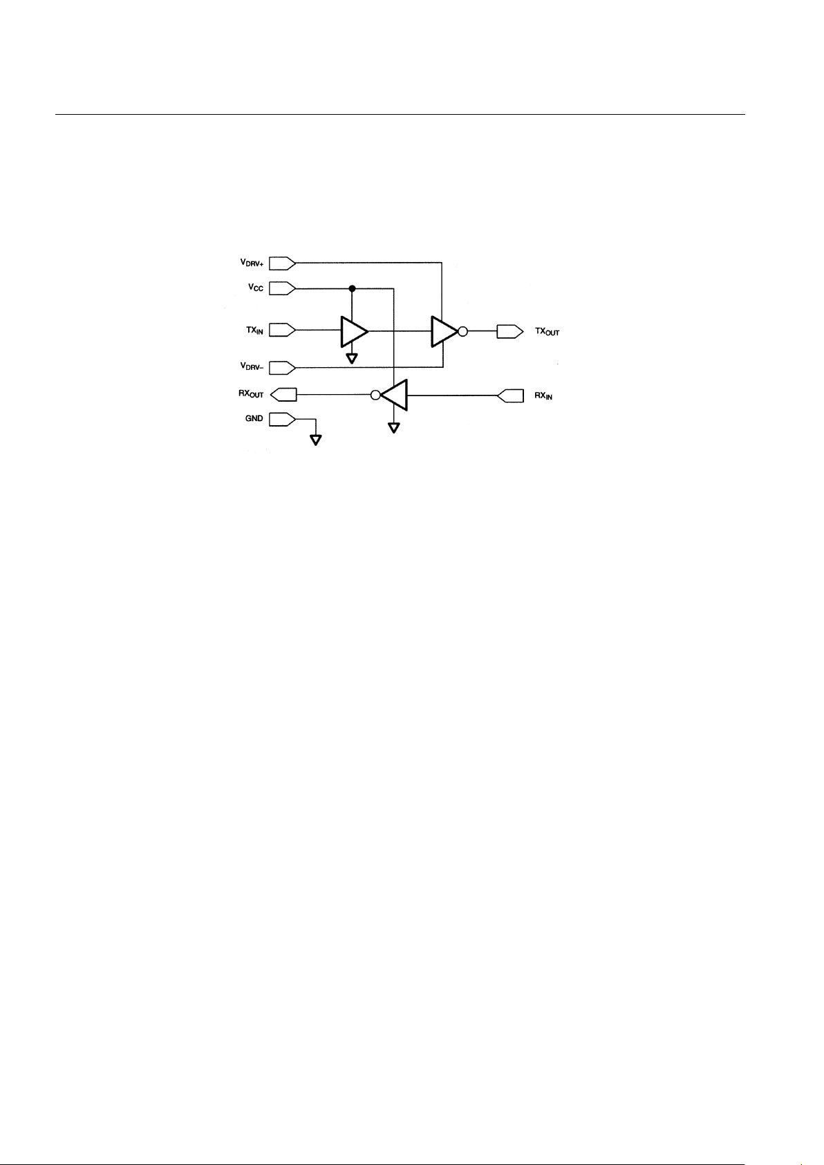
DS276 BLOCK DIAGRAM Figure 1
APPLICATIONS INFORMATION
The DS276 is designed as a low-cost, RS-232-E interface expressly tailored for the unique requirements
of battery-operated handheld products. As shown in the electrical specifications, the DS276 draws
exceptionally low operating and static current. During normal operation when data from the handheld
system is sent from the TX
OUT
output, the DS276 only draws significant V
DRV+
current when TX
OUT
transitions positively (spacing). This current flows primarily into the RS-232 receiver’s 3-7 kΩ=load at
the other end of the attaching cable. When TX
OUT
is marking (a negative data signal), the V
DRV+
current
falls dramatically since the negative voltage is provided by the transmit signal from the other end of the
cable. This represents a large reduction in overall operating current, since t ypical RS-232 interface chips
use charge-pump circuits to establish both positive and negative levels at the transmit driver output. To
obtain the lowest power consumption from the DS276, observe the following guidelines: First, to
minimize V
DRV+
current when connected to an RS-232 port, always maintain TXIN at a logic 1 wh en data
is not being transmitted (idle state). This will force TX
OUT
into the marking state, minimizing V
DRV+
current. Second, V
DRV+
current will drop significantly when VCC is grounded. Therefore, if V
DRV+
is
derived independently from VCC (for example connected to a 9V battery), the logic supply voltage can b e
turned off to achieve the lowest possible power state.
FULL-DUPLEX OPERATION
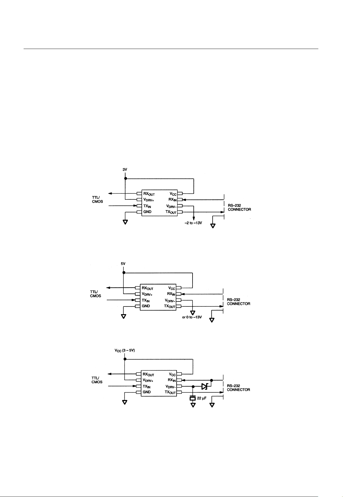
The DS276 is intended for full-duplex operation using the full-duplex circuit shown in Figure 4 to
generate a negative rail from RXIN. The 22 µF capacitor forms a negative-charge reservoir; consequentl y,
when the TXD line RXIN is spacing (positive), TX
OUT
still has a negative source available for a time
period determined by the capacitor and the load resistance at the other end (3-7 kΩ).
SUPPLY VOLTAGE OPTIONS
The DS276 is intended primarily for use in single supply 3- or 5- volts systems. However, several supply
configurations are possible.
3V OPERATION
The simplest configuration is to use a single 3V supply for VCC and V
drv+
, and connect V
drv-
to ground.
This will result in the lowest power consumption and will give adequate serial communication between

DS276
4 of 11
two similar devices over short distances, and into larger loads than the 3 kΩ=RS-232 standard (Figure 2).
If V
drv+
is increased to 5V, and V
drv-
decreased (to less than -2V) communication with standard RS-232
devices is possible, although of course the output voltage swing of the DS276 remains below the RS-232
specification. The V
drv-
supply can be derived using the “stealing” technique shown in Figure 4.
5V OPERATION
The use of a single 5V supply for VCC and V
drv+
, and V
drv-
derived using the circuit in Figure 4 can
produce reliable communication with standard RS-232 devices, although the DS276 output voltage
swings are below the RS-232 minimum (Figure 3).
Increasing the magnitude of the voltage to V
drv+
to 10 volts or more will result in “true” RS-232 output
voltage levels.
SINGLE 3V OPERATION Figure 2
(See Note 3)
SINGLE 5V OPERATION Figure 3
(not true RS-232)
(See Note 1 and 3)
"STEALING" NEGATIVE SUPPLY Figure 4
(See Note 2)
 Loading...