dallas semiconductor DS2760 service manual
r
www.dalsemi.com
C
V
PRELIMINARY
DS2760
High Precision Li-Ion Battery Monito
FEATURES
Li-Ion safety circuit
- Overvoltage protection
- Overcurrent/short circuit protection
- Undervoltage protection
Available in two configurations:
- Internal 25 mΩ sense resistor
- External user-selectable sense resistor
Current measurement
- 12-bit bi-directional measurement
- Internal sense resistor configuration:
0.625 mA LSB and ±1.8A dynamic range
- External sense resistor configuration:
15.625 µV LSB and ±64 mV dynamic range
Current accumulation
- Internal sense resistor: 0.25 mAhr LSB
- External sense resistor: 6.25 µVhr LSB
Voltage measurement with 4.88 mV resolution
Temperature measurement using integrated
sensor with 0.125°C resolution
System power management and control feature
support
32 bytes of lockable EEPROM
16 bytes of general purpose SRAM
Dallas 1-Wire
device address
Low power consumption:
- Active current: 80 µA max
- Sleep current: 2 µA max
®
interface with unique 64-bit
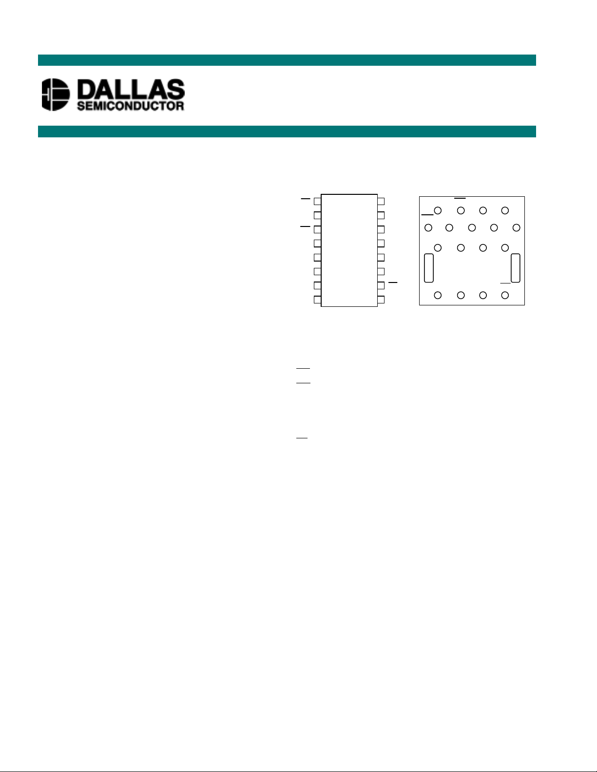
PIN ASSIGNMENT
CC VIN
1
1
2
2
PLS
3
2
DC
SNS
SNS
SNS
4
5
6
DQ
7
IS2
8
DS2760
16-Pin TSSOP Package
16
15
14
13
12
11
10
PLS CC VIN VDD
VDD
PIO
VSS
VSS
VSS
PS
IS1
9
DC NC NC NC PIO
SNS
NC N
Probe
SNS
DQ IS2 IS1 PS
DS2760
Flip-Chip Packaging
PIN DESCRIPTION
- Charge control output
CC
- Discharge control output
DC
DQ - Data input/output
PIO - Programmable I/O pin
PLS - Battery pack positive terminal input
- Power switch sense input
PS
VIN - Voltage sense input
VDD- Power supply input (2.5V-5.5V)
VSS - Device ground
SNS - Sense resistor connection
IS1 - Current sense input
IS2 - Current sense input
NC - Not connected
SNS Probe – Do not connect
VSS Probe – Do not connect
SS
VSS
1 of 25 092000

DS2760
ORDERING INFORMATION
DS2760E TSSOP, External Sense
Res., 4.35V V
OV
DS2760EA TSSOP, External Sense
Res., 4.275V V
OV
DS2760T DS2760E on Tape & Reel
DS2760TA DS2760EA on Tape &
Reel
DS2760E-025 TSSOP, 25 mΩ Sense
Res., 4.35V V
OV
DS2760EA-025 TSSOP, 25 mΩ Sense
Res., 4.275V V
OV
DS2760T-025 DS2760E-025 in Tape &
Reel
DS2760TA-025 DS2760EA-025 in Tape
& Reel
DS2760X Flipchip, Ext. Sense Res.,
T&R, 4.35V V
OV
DS2760XA Flipchip, Ext. Sense Res.,
T&R, 4.275V V
OV
DS2760X-025 Flipchip, 25 mΩ Sense
Res., T&R, 4.35V V
OV
DS2760XA-025 Flipchip, 25 mΩ Sense
Res., T&R, 4.275V V
OV
DESCRIPTION
The DS2760 High Precision Li-Ion Battery Monitor is a data acquisition, information storage, and safety
protection device tailored for cost-sensitive battery pack applications. This low-power device integrates
precise temperature, voltage, and current measurement, nonvolatile data storage, and Li-Ion protection
into the small footprint of either a TSSOP package or flip-chip. The DS2760 is a key component in
applications including remaining capacity estimation, safety monitoring, and battery-specific data storage.
Via its 1-Wire interface, the DS2760 gives the host system read/write access to status and control
registers, instrumentation registers, and general purpose data storage. Each device has a factoryprogrammed 64-bit net address which allows it to be individually addressed by the host system,
supporting multi-battery operation.
The DS2760 is capable of performing temperature, voltage and current measurement to a resolution
sufficient to support process monitoring applications such as battery charge control, remaining cap acity
estimation, and safety monitoring. Temperature is measured using an on-chip sensor, eliminating the need
for a separate thermistor. Bi-directional current measurement and accumulation are accomplished using
either an internal 25 mΩ sense resistor or an external device. The DS2760 also features a pro grammable
I/O pin that allows the host system to sense and control other electronics in the pack, including switches,
vibration motors, speakers and LEDs.
Three types of memory are provided on the DS2760 for battery information storage: EEPROM, lockable
EEPROM and SRAM. EEPROM memory saves important battery data in true nonvolatile memory that
is unaffected by severe battery depletion, accidental shorts or ESD events. Lock able EEPROM becomes
ROM when locked to provide additional security for unchanging battery data. SRAM provides
inexpensive storage for temporary data.
2 of 25
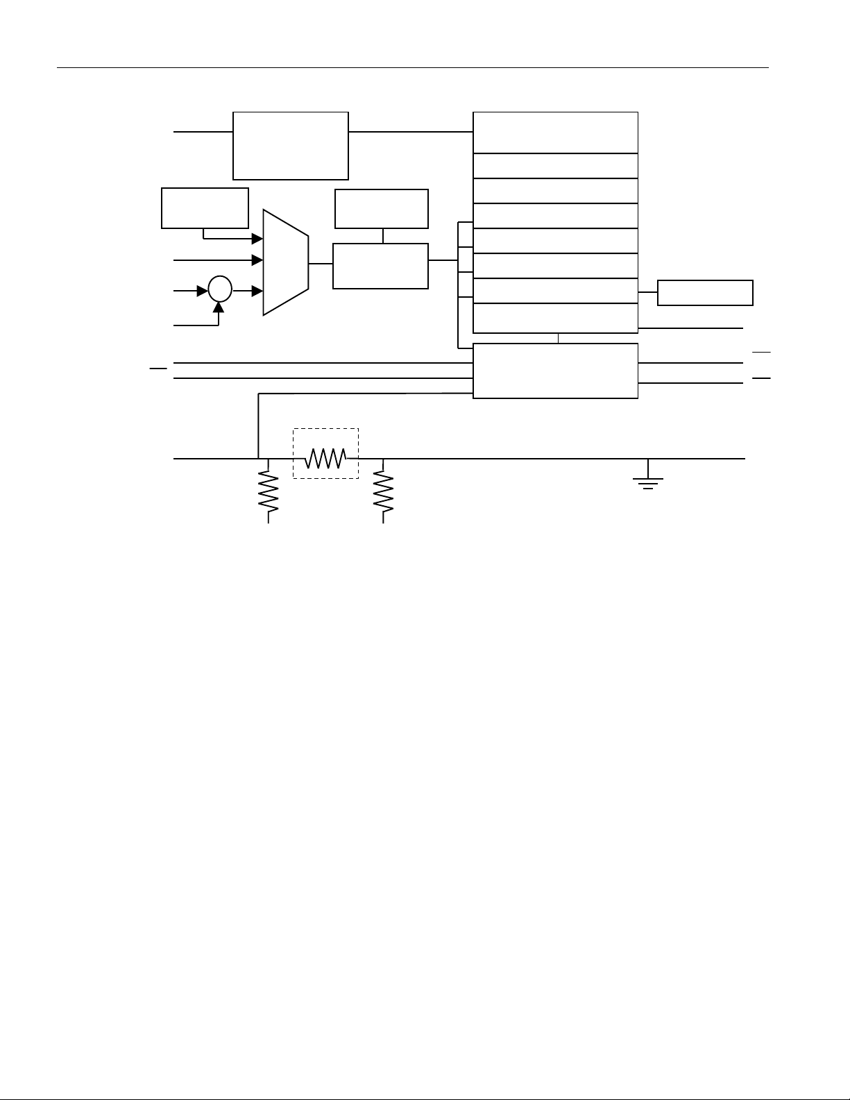
BLOCK DIAGRAM – Figure 1
Y
DS2760
DQ
VIN
IS1
IS2
PLS
PS
SNS
THERMAL
SENSE
+
1-WIRE
INTERFACE
ADDRESS
MUX
-
AND
LOCKABLE EEPROM
VOLTAGE
REFERENCE
ADC
ACCUM. CURRENT
STATUS / CONTROL
LI-ION PROTECTION
internal sense resistor configuration only
25 mΩ
REGISTERS AND
USER MEMOR
SRAM
TEMPERATURE
VOLTAGE
CURRENT
chip ground
TIMEBASE
PIO
CC
DC
VSS
IS2 IS1
3 of 25

DETAILED PIN DESCRIPTION – Table 1
SYMBOL DESCRIPTION
DS2760
CC
Charge Protection Control Output. Controls an external p-channel high-side charge
protection FET.
DC
Discharge Protection Control Output. Controls an external p-channel high-side
discharge protection FET.
DQ
Data Input/Out. 1-Wire data line. Open-drain output driver. Connect this pin to the
DATA terminal of the battery pack. Pin has an internal 1 µA pull-down for sensing
disconnection.
PIO
Programmable I/O Pin. Used to control and monitor user-defined external circuitry.
Open drain to VSS.
PLS
Battery Pack Positive Terminal Input. The device monitors the state of the battery
pack’s positive terminal through this pin in order to detect events such as the attachment
of a charger or the removal of a short circuit.
PS
Power Switch Sense Input. The device wakes up from Sleep Mode when it senses the
closure of a switch to VSS on this pin. Pin has an internal 1 µA pull-up.
VIN Voltage Sense Input. The voltage of the Li-Ion cell is monitored via this input pin.
VDD
Power Supply Input. Connect to the positive terminal of the Li-Ion cell through a
decoupling network.
VSS
Device Ground. Connect directly to the negative terminal of the Li-Ion cell. For the
external sense resistor configuration, connect the sense resistor between VSS and SNS.
SNS Sense Resistor Connection. Connect to the negative terminal of the battery pack. In the
internal sense resistor configuration, the sense resistor is connected between VSS and
SNS.
IS1
IS2
Current Sense Input. This pin is internally connected to VSS through a 4.7 kΩ resistor.
Connect a 0.1µF capacitor between IS1 and IS2 to complete a low-pass input filter.
Current Sense Input. This pin is internally connected to SNS through a 4.7 kΩ resistor.
4 of 25
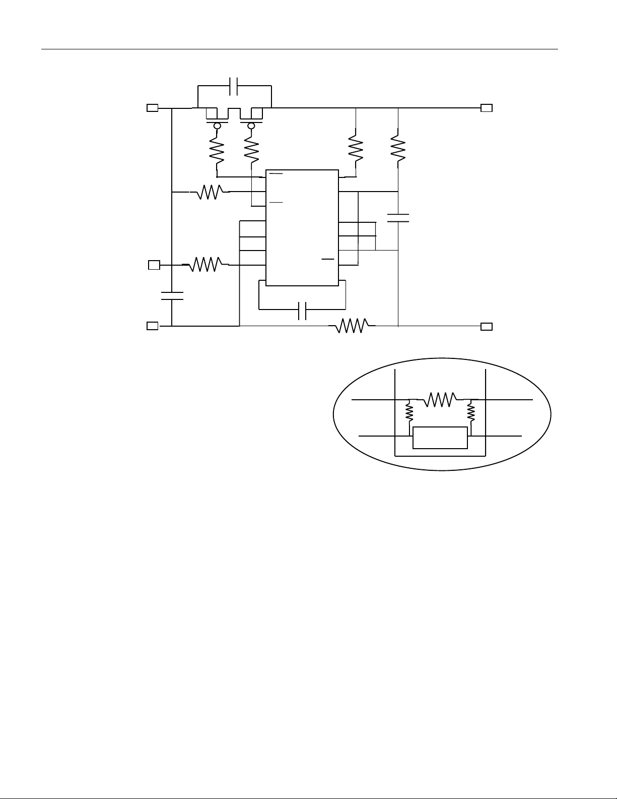
APPLICATION EXAMPLE – Figure 2
0
(1)
(2)
102
DS2760
PACK+
DATA
PACK-
1
1 kΩ
150Ω
150
2
BAT+
1 kΩ
1kΩ
150Ω
DS2760
CC
PLS
DC
SNS
SNS
Ω
SNS
DQ
IS2
VIN
VDD
PIO
VSS
VSS
VSS
PS
IS1
104
104
BAT-
R
SENS
DS2760
SNS
VSS
1 – R
2 – R
is present for external sense resistor configurations only
SENS
SENSINT
is present for internal sense resistor configurations only
R
R
KS
IS2 IS1
SENSINT
4.7 kΩ
voltage
R
KS
4.7 kΩ
sense
5 of 25

DS2760
POWER MODES
The DS2760 has two power modes: Active and Sleep. While in Active Mode, the DS2760 continually
measures current, voltage and temperature to provide data to the host system and to support current
accumulation and Li-ion safety monitoring. In Sleep Mode, the DS2760 ceases these activities. The
DS2760 enters Sleep Mode when either of the following conditions occurs:
• the PMOD bit in the Status Register has been set to 1 and the DQ line is low for
longer than 2 seconds (pack disconnection)
• the voltage on VIN drops below undervoltage threshold VUV for t
• the pack is disabled through the issuance of a SWAP command (SWEN bit =1)
The DS2760 returns to Active Mode when any of the following occurs:
• the PMOD bit has been set to 1 and the SWEN bit is set to 0 and the DQ line is pulled
high (pack connection)
• the PS pin is pulled low (power switch)
• the voltage on PLS becomes greater than the voltage on VIN (charger connection) with the
SWEN bit set to 0
• the pack is enabled through the issuance of a SWAP command (SWEN bit =1)
The DS2760 defaults to Active Mode when power is first applied.
(cell depletion)
UVD
LI-ION PROTECTION CIRCUITRY
During Active Mode, the DS2760 constantly monitors cell voltage and current to protect the batte ry from
overcharge (overvoltage), overdischarge (undervoltage) and excessive charge and discharge currents
(overcurrent, short circuit). Conditions and DS2760 responses are described in the sections below and
summarized in Table 2 and Figure 3.
LI-ION PROTECTION CONDITIONS AND DS2760 RESPONSES – Table 2
ActivationCondition
Name
Overvoltage V
Undervoltage V
Threshold Delay Response
IN
IN
> V
< V
OV
UV
t
OVD
t
UVD
CC
CC, DC
high
high,
Sleep Mode
Overcurrent, Charge V
Overcurrent, Discharge V
Short Circuit V
VIS = V
IS1
– V
. Logic high = V
IS2
IS
IS
SNS
< -V
PLS
(1)
> V
> V
OC
OC
(1)
SC
t
OCD
t
OCD
t
SCD
for CC and VDD for
CC, DC
DC
.
high
high
DC
high
DC
All voltages are with respect to VSS. I
references current delivered from pin SNS.
(1) for the internal sense resistor configuration, the overcurrent thresholds are expressed in terms of
current: I
(2) with test current I
(3) with test current I
> IOC for charge direction and I
SNS
current flowing from PLS to VSS (pull-down on PLS)
TST
current flowing from VDD to PLS (pull-up on PLS)
TST
< -IOC for discharge direction
SNS
Release
Threshold
V
< V
IN
CE
V
> VDD
PLS
(charger connected)
V
< VDD - V
PLS
V
> VDD - V
PLS
V
> VDD - V
PLS
TP
TP
TP
(2)
(3)
(3)
SNS
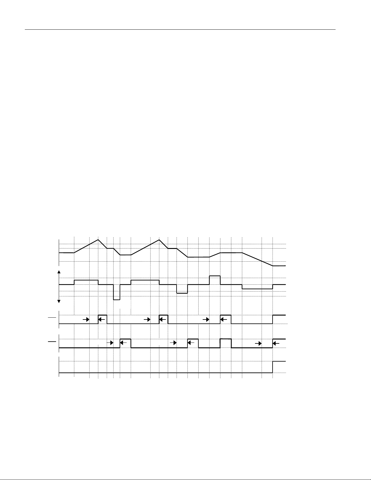
Overvoltage. If the voltage of the cell exceeds overvoltage threshold VOV for a period longer than
overvoltage delay t
, the DS2760 shuts off the external charge FET and sets the OV flag in the
OVD
Protection Register. When the cell voltage falls below charge enable threshold VCE, the DS2760 turns the
charge FET back on (unless another protection condition prevents it). Discharging remains enabled
during overvoltage.
6 of 25
DS2760
SC
OC
U
Undervoltage. If the voltage of the cell drops below undervoltage threshold VUV for a period longer than
undervoltage delay t
, the DS2760 shuts off the charge and discharge FETs, sets the UV flag in the
UVD
Protection Register, and enters Sleep Mode.
Overcurrent, Charge Direc tion. The voltage difference between th e IS1 pin and the IS2 pin (V
– V
) is the filtered voltage drop across the current sense resistor. If VIS exceeds overcurrent threshold
IS2
VOC for a period longer than overcurrent delay t
, the DS2760 shuts off both external FETs and sets the
OCD
IS
= V
IS1
COC flag in the Protection Register. The charge current path is not re-established until the voltage on the
PLS pin drops below VDD – V
. The DS2760 provides a test current of value I
TP
from PLS to VSS to
TST
pull PLS down when the offending charge current source has been removed.
Overcurrent, Discharge Direction. If VIS is less than -VOC for a period longer than t
, the DS2760
OCD
shuts off the external discharge FET and sets the DOC flag in the Protection Register. The discharge
current path is not re-established until the voltage on PLS rises above VDD - VTP. The DS2760 provides
a test current of value I
from VDD to PLS to pull PLS up when the offending low-impedance load has
TST
been removed.
Short Circuit. If the voltage on the SNS pin with respect to VS S exceeds short cir cuit threshold VSC for
a period longer than short circuit delay t
, the DS2760 shuts off the external discharge FET and sets the
SCD
DOC flag in the Protection Register. The discharge current path is not re-established until the voltage on
PLS rises above VDD - VTP. The DS2760 provides a test current of value I
from VDD to PLS to pull
TST
PLS up when the short circuit has been removed.
LITHIUM-ION PROTECTION CIRCUITRY EXAMPLE WAVEFORMS – Figure 3
V
OV
V
CELL
charge
V
discharge
CC
IS
(1)
t
OVD
t
OVD
t
OCD
V
V
V
0
-V
-V
V
VSS
CE
UV
OC
OC
SC
PLS
DC
t
D
t
D
t
VD
Sleep
Mode
(1) To allow the device to react quickly to short circuits, detection is actually done on the SNS pin rather
than on the filtered IS1 and IS2 pins. The actual short circuit detect condition is V
SNS
> VSC.
7 of 25
VDD
VSS
active
inactive

DS2760
r
r
Summary. All of the protection conditions described above are OR'ed together to affect the CC and
DC
outputs.
= (Undervoltage) or (Overcurrent, EITHER Direction) or (Short Circuit) or
DC
(Protection Register bit DE = 0) or (Sleep Mode)
= (Overvoltage) or (Overcurrent, Charge Direction) or (Protection Register bit CE = 0) or
CC
(Sleep Mode)
CURRENT MEASUREMENT
In the Active Mode of operation, the DS2760 continually measures the current flow into and out of the
battery by measuring the voltage drop across a current sense resistor. The DS2760 is available in two
configurations: (1) internal 25 mΩ current sense resistor, and (2) external user-selectable sense resistor. In
either configuration, the DS2760 considers the voltage difference between pins IS1 and IS2 (VIS = V
V
) to be the filtered voltage drop across the sense resistor. A positive VIS value indicat es current is
IS2
flowing into the battery (charging), while a negative VIS value indicates current is flowing out of the
battery (discharging). Note than when an external sense resistor is used, one end of the resistor must be
wired directly to VSS (the negative terminal of the cell) for proper operation of the current measurement
circuitry.
IS1
–
VIS is measured with a signed resolution of 12-bit s. Measurements are placed in the Current Register in
two’s-complement format. Currents outside the range of the register are reported at the limit of the range.
The format of the Current Register is shown in Figure 4.
For the internal sense resistor configuration, the DS2760 maintains the Current Register in units of Amps,
with a resolution of 0.625 mA and full scale range of no less than ±1.8A (see Note 7 on IFS spec for more
details). The DS2760 automatically compensates for internal sense resistor process variations and
temperature effects when reporting current.
For the external sense resistor configuration, the DS2760 writes the measured VIS voltage to the Current
Register, with a resolution of 15.625 µV and a full scale range of ±64 mV.
CURRENT REGISTER FORMAT – Figure 4
MSB—Address 0E LSB—Address 0F
S2112
1029
2827262
MSb LSb MSb LSb
5
2423222120XXX
Units: 0.625 mA for internal sense resisto
15.625 µV for external sense resisto
CURRENT ACCUMULATOR
The Current Accumulator facilitates remaining capacity estimation by tracking the net current flow into
and out of the battery. Current flow into the battery increments the Current Accumulator while current
flow out of the battery decrements it. Data is maintained in the Current Accumulator in two’scomplement format. The format of the Current Accumulator is shown in Figure 5.
8 of 25
 Loading...