Dallas Semiconductor DS2480S Datasheet
DS2480
FEATURES
• Universal, common–ground serial port to 1–Wire
line driver for MicroLANTM applications
TM
• Works with all iButtons and MicroLAN–compatible
1–Wire slave devices
• Communicates at regular and Overdrive 1–Wire
speed and serial port data rates of 9600 (default),
19200, 57600 and 1 15200 bps
• Supports 12V EPROM programming and stiff 5V
pull–up for Crypto iButton, sensors and EEPROM
• Self–calibrating time base with ±5% tolerance for
serial and 1–Wire communication
• Slew rate controlled 1–Wire pull–down and active
pull–up to accommodate long lines and reduce radiation
• User–selectable RXD/TXD polarity minimizes com-
ponent count when interfacing to 5V based RS232
systems or directly to UARTs
• Programmable 1–Wire timing and driver characteris-
tics accommodate a wide range of MicroLAN configurations at regular speed
• Smart protocol combines data and control information
without requiring extra pins
• Compatible to optical, IR and RF to RS232 converters
• Low cost 8–pin SOIC surface mount package
• Operates over 4.5V to 5.5V from –40°C to +85°C
Serial 1–Wire
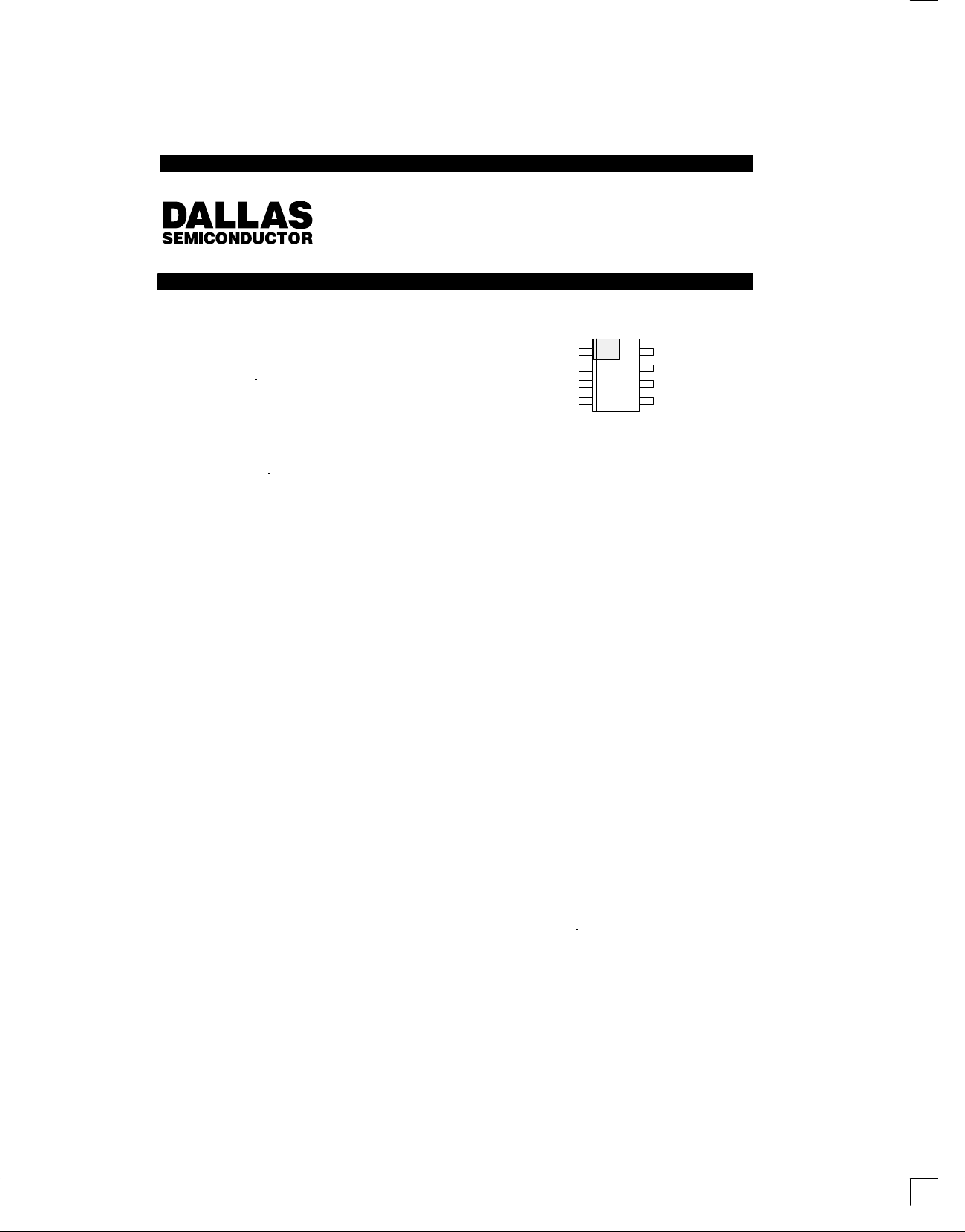
PIN ASSIGNMENT
GND
1–W
NC
V
DD
PIN DESCRIPTION
GND Ground
1–W 1–Wire Input/Output
NC No Connection
V
DD
V
PP
POL RXD/TXD Polarity Select
TXD Serial Data from UART
RXD Serial Data to UART
ORDERING INFORMATION
DS2480S 8–pin SOIC
TM
Line Driver
RXD
8
1
TXD
7
2
POL
6
3
5
4
8–PIN SOIC
(150 MIL)
4.5 to 5.5 Volts
Optional EPROM
Programming Voltage
V
PP
DS2480
DESCRIPTION
The DS2480 is a serial port to 1–Wire interface chip that
supports standard and Overdrive speeds. It connects
directly to UART s and 5V RS232 systems. Interfacing to
RS232C (±12V levels) requires a passive clamping circuit and one 5V to ±12V level translator. Internal timers
relieve the host of the burden of generating the time–
critical 1–Wire communication waveforms. In contrast
to the DS9097(E) where a full character must be sent by
the host for each 1–Wire time slot, the DS2480 can
translate each character into eight 1–Wire time slots
thereby increasing the data throughput significantly. In
addition, the DS2480 can be set to communicate at four
different data rates including 1 15.2 kbps, 57.6 kbps and
19.2 kbps with 9.6 kbps being the power–on default.
Command codes received from the host’s crystal controlled UART serve as a reference to continuously calibrate the on–chip timing generator . The DS2480 uses a
unique protocol that merges data and control information without requiring control pins. This approach maintains compatibility to off–the–shelf serial to wireless
converters allowing easy realization of 1–Wire media
jumpers. The various control functions of the DS2480
are optimized for MicroLAN 1–Wire networks and support the special needs of all current 1–Wire devices
including the Crypto i
Memories, EEPROM devices and 1–Wire Thermometers.
Button, EPROM–based Add–Only
042498 1/26
DS2480
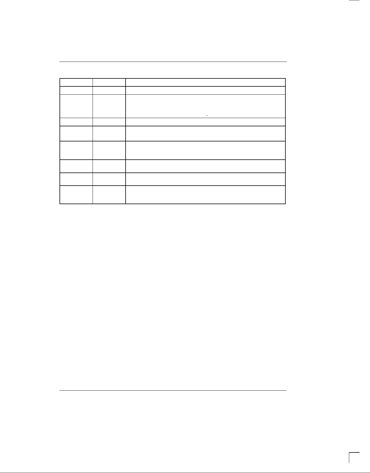
DETAILED PIN DESCRIPTION
PIN SYMBOL DESCRIPTION
1 GND Ground Pin: common ground reference and ground return for 1–Wire bus
2 1–W 1–Wire Input/Output Pin: 1–Wire bus with slew–rate–controlled pull–down,
active pull–up, ability to switch in V
through a low–impedance path to program EEPROM, perform a temper-
in V
DD
ature conversion or operate the Crypto i
3 NC No Connection Pin.
4 V
DD
Power Input Pin: power supply for the chip and 1–Wire pull–up voltage. 5V ±
10%; may be derived from 12V VPP with an external voltage regulator.
5 V
PP
EPROM Programming Voltage: 12V supply input for EPROM programming;
if EPROM programming is not required, this pin must be tied to V
come up before V
DD
.
6 POL RXD/TXD Polarity Select: RXD/TXD polarity select; tied to GND for RS232
(12V or 5V) connection, tied to V
7 TXD Serial Data from UART : data input from host (inverted or true); maximum volt-
age swing –0.3V to V
+ 0.3V; for logic thresholds see DC specifications.
DD
8 RXD Serial Data to UART: signal output to host; push–pull driver with CMOS com-
patible levels; for true ±12V RS232 systems an external level–translator must
be provided.
to program EPROM, and ability to switch
PP
Button.
for direct connection to UART chip.
DD
. VPP must
DD
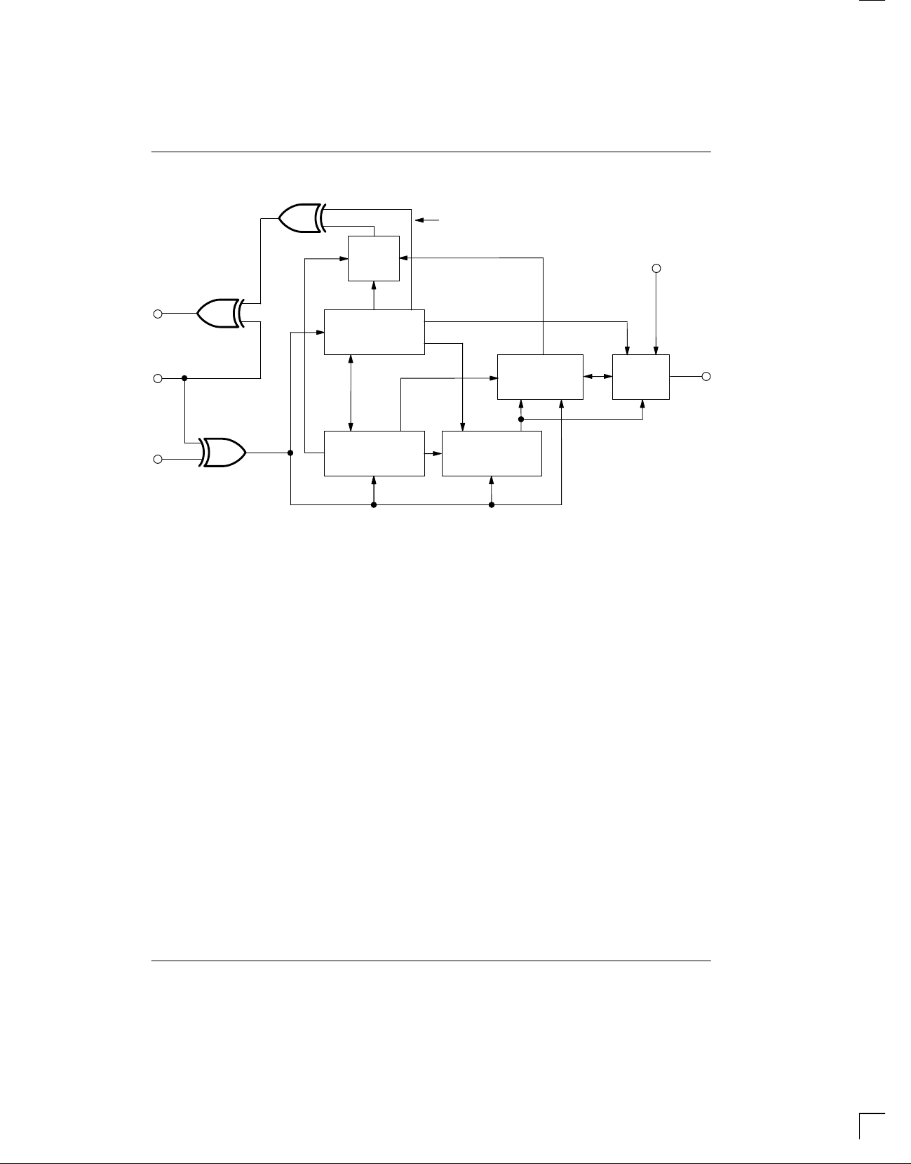
OVERVIEW
The DS2480 directly interfaces a 5V serial communication port with its lines TXD (transmit) and RXD (receive)
to a 1–Wire bus. In addition the device performs a speed
conversion allowing the data rate at the communication
port to be different from the 1–Wire date rate. Several
parameters relating to the 1–Wire port and its timing as
well as the communication speed at both the port and
the 1–Wire bus are configurable. The circuit to achieve
these functions is outlined in Figure 1, Block Diagram.
The device gets its input data from the serial communication port of the host computer through pin TXD. For
compatibility with active–high as well as active–low systems, the incoming signal can be inverted by means of
the polarity input POL. The polarity chosen by hard–wiring the logic level of this pin is also valid for the output pin
RXD. If for minimizing the interface hardware an asymmetry between RXD and TXD is desired, this can be
achieved by setting the most significant bit of the Speed
Control parameter to a 1 (see Configuration Parameter
Value Codes). With the MS bit of the speed control set to
1, the polarity at TXD is still selected by the logic level at
POL, but the polarity at RXD will be the opposite of what
the logic level at POL specifies.
As data enters the core of the DS2480’s logic circuitry, it
is analyzed to separate data and command bytes and to
calibrate the device’s timing generator . The timing generator controls all speed relations of the communication
interface and the 1–Wire bus as well as the wave forms
on the 1–Wire bus.
Command bytes either affect the configuration setting
or generate certain wave forms on the 1–Wire bus. Data
bytes are simply translated by the protocol converter
into the appropriate 1–Wire activities. Each data byte
generates a return byte from the 1–Wire bus, that is
communicated back to the host through the RXD pin as
soon as the activity on the 1–Wire bus is completed.
The 1–Wire driver shapes the slopes of the 1–Wire
wave forms, applies programming pulses or strong
pull–up to 5 volts and reads the 1–Wire bus using a non–
TTL threshold to maximize the noise margin for best
performance on large 1–Wire MicroLAN networks.
042498 2/26
DS2480 BLOCK DIAGRAM Figure 1
RXD
CONFIGURATION
POL
MUX
REGISTER
MS BIT OF SPEED CONTROL
(1 = RXD IS INVERTED)
PROTOCOL
CONVERTER
1–WIRE
DRIVER
DS2480
V
PP
1–W
TXD
PROTOCOL
PROTOCOL
ANALYZER
ANALYZER
DEVICE OPERATION
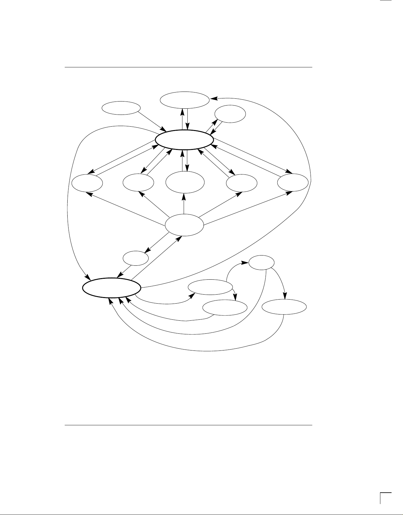
The DS2480 can be described as a complex state
machine with two static and several dynamic states.
Two device–internal flags as well as functions assigned
to certain bit positions in the command codes determine
the behavior of the chip, as shown in the state transition
diagram (Figure 2). The DS2480 requires and generates a communication protocol of 8 data bits per character, 1 stop bit and no parity. It is permissible to use two
stop bits on the TXD line. However, the DS2480 will only
assert a single stop bit on RXD.
When powering up, the DS2480 performs a master
reset cycle and enters the Command Mode, which is
one of the two static states. The device now expects to
receive one 1–Wire reset command on the TXD line
sent by the host at a data rate of 9600 bits per second
(see section Communication Commands for details).
This command byte is required solely for calibration of
TIMING
GENERATOR
the timing generator the DS2480 and is not translated
into any activity on the 1–Wire bus. After this first command byte the device is ready to receive and execute
any command as described later in this document.
A master reset cycle can also be generated by means of
software. This may be necessary if the host for any reason has lost synchronization with the device. The
DS2480 will perform a master reset cycle equivalent to
the power–on reset if it detects start polarity in place of
the stop bit. The host has several options to generate
this condition. These include making the UART generate a break signal, sending a NULL character at a data
rate of 4800 bps and sending any character with parity
enabled and selecting space polarity for the parity bit.
As with the power–on reset, the DS2480 requires a
1–Wire reset command sent by the host at a data rate of
9600 bps for calibration.
042498 3/26
DS2480
STATE TRANSITION DIAGRAM Figure 2
E1h
RESET
SOFTWARE
MASTER RESET
110XSS01
N.C.
110XSS01
111T11Q1
PULSE
TX E3h
N.C.
POWER OFF
N.C.
111T11Q1
E3h
CODE = E3h
INACTIVE
POWER
ON
ARRIVAL
COMMAND MODE
0ZZZVVV1
N.C.
CONFIGURATION
0ZZZVVV1
CHECK
MODE
ARRIVAL
N.C.
101HSS01
N.C.
ACC. OFF
TX
CODE
SEARCH
ACCEL.
101HSS01
100VSSP1
100VSSP1
TX BYTE
N.C.
POWER OFF
SINGLE BIT
FUNCTION
STR. PULL–UP
ARMED
DATA MODE
ALL OTHER
CODES
N.C. = UNCONDITIONAL
LEGEND: V BINARY VALUE (TYPE OF WRITE TIME SLOT)
042498 4/26
SS 1–WIRE SPEED SELECTION CODE
P IF LOGIC 1, GENERATES STRONG PULL–UP TO 5V IMMEDIATELY FOLLOWING THE TIME SLOT
T TYPE OF PULSE; 0 = STRONG PULL–UP (5V), 1 = PROGRAMMING PULSE (12V)
Q 1 = ARM STRONG PULL–UP AFTER EVERY BYTE; 0 = DISARM
H SEARCH ACCELERATOR CONTROL; 1 = ACCELERATOR ON, 0 = ACCELERATOR OFF
ZZZ CONFIGURATION PARAMETER CODE (WRITE), 000 = READ CONFIGURATION PARAMETER
VVV CONFIGURATION PARAMETER VALUE CODE (WRITE), CONFIGURATION PARAMETER CODE (READ)
X DON’T CARE
ACCELERATOR FLAG
N.C.
STR. PULL–UP NOT ARMED
CHECK SEARCH
PERFORM SEARCH
SEQUENCE
ACC.ON
GENERATE STRONG
PULL–UP TO 5V
N.C.

DS2480
After the DS2480 has reached the command mode, the
host can send commands such as 1–Wire Reset, Pulse,
Configuration, Search Accelerator and Single Bit functions or switch over to the second static state called
Data Mode. In data mode the DS2480 simply converts
bytes it receives at the TXD pin into their equivalent
1–Wire wave forms and reports the results back to the
host through the RXD pin. If the Search Accelerator is
on, each byte seen at TXD will generate a 12–bit
sequence on the 1–Wire bus (see section Search
Accelerator for details). If the Strong Pull–up to 5V is
enabled (see Pulse command) each byte on the 1–Wire
bus will be followed by a pause of predefined duration
where the bus is pulled to 5V via a low impedance transistor in the 1–Wire driver circuit.
While being in the Data Mode the DS2480 checks each
byte received from the host for the reserved code that is
used to switch back to Command Mode. To be able to
write any possible code (including the reserved one) to
the 1–Wire bus, the transition to the Command Mode is
as follows: After having received the code for switching
to Command Mode, the device temporarily enters the
Check Mode where it waits for the next byte. If both
bytes are the same, the byte is sent once to the 1–Wire
bus and the device returns to the Data Mode. If the
second byte is different from the reserved code, it will be
executed as command and the device finally enters the
Command Mode. As a consequence, if the reserved
code that normally switches to Command Mode is to be
written to the 1–Wire bus, this code byte must be sent
twice (duplicated). This detail must be considered carefully when developing software drivers for the DS2480.
After having completed a memory function with a device
on the 1–Wire bus it is recommended to issue a Reset
Pulse. This means that the DS2480 has to be switched
to Command mode. The host then sends the appropriate command code and continues performing other
tasks. If during this time a device arrives at the 1–Wire
bus it will generate a presence pulse. The DS2480 will
recognize this unsolicited presence pulse and notify the
host by sending a byte such as XXXXXX01b. The Xs
represent undefined bit values. The fact that the host
receives the byte unsolicited together with the pattern
01b in the least significant two bits marks the bus arrival.
If the DS2480 is left in Data Mode after completing a
memory function command it will not report any bus
arrival to the host.
COMMAND CODE OVERVIEW
The DS2480 is controlled by a variety of commands. All
command codes are 8 bits long. The most significant bit
of each command code distinguishes between communication and configuration commands. Configuration
commands access the configuration registers. They
can write or read any of the configurable parameters.
Communication commands use data of the configuration register in order to generate activity on the 1–Wire
bus and/or (dis)arm the strong pull–up after every byte
or (de)activate the Search Accelerator without generating activity on the 1–Wire bus. Details on the command
codes are included in the State Transition diagram
(Figure 2). A full explanation is given in the subsequent
sections Communication Commands and Configuration Commands.
In addition to the command codes explained in the subsequent sections the DS2480 understands the following reserved command codes:
E1h switch to Data Mode
E3h switch to Command Mode
F1h pulse termination
Except for these reserved commands, the Search
Accelerator control and the first byte after power–on
reset or master reset cycle, every legal command byte
generates a response byte. The pulse termination code
triggers the response byte of the terminated pulse command. Illegal command bytes do not generate a command response byte.
Once the device is switched back from Data Mode to
Command Mode one must not repeat the E3h command while the Command Mode is still active.
COMMUNICATION COMMANDS
The DS2480 supports four communication function
commands: Reset, Single Bit, Pulse, and Search Accelerator control. Details on the assignment of each bit of
the command codes are shown in Table 1. The corresponding command response bytes are detailed in
Table 2. The Reset, Search Accelerator Control and
Single Bit commands include bits to select the 1–Wire
communication speed (regular, flexible regular, Overdrive). Even if a command does not generate activity on
the 1–Wire bus, these bits are latched inside the device
and will take effect immediately.
042498 5/26

DS2480
COMMUNICATION COMMAND CODES Table 1
FUNCTION BIT 7 BIT 6 BIT 5 BIT 4 BIT 3, BIT 2 BIT 1 BIT 0
Single Bit 1 0 0 0 = write 0
1 = write 1
00 reg. speed
01 flex. speed
See Text 1
10 OD. speed
11 reg. speed
Search
Accelerator
Control
1 0 1 0 = accelerator off
1 = accelerator on
See Text
00 reg. speed
01 flex. speed
10 OD. speed
0 1
11 reg. speed
Reset 1 1 0 (don’t care) 00 reg. speed
0 1
01 flex. speed
10 OD. speed
11 reg. speed
Pulse 1 1 1 0 = 5V strong pull–up
11 pulse See Text 1
1 = 12V prog. pulse
COMMUNICATION COMMAND RESPONSE Table 2
FUNCTION BIT 7 BIT 6 BIT 5 BIT 4 BIT 3 BIT 2 BIT 1 BIT 0
Single Bit 1 0 0 same as sent 1–Wire read back,
Reset 1 1 See
01000 = 1–Wire shorted
Text
Pulse 1 1 1 same as sent undefined
both bits same value
01 = presence pulse
10 = alarming presence
pulse
11 = no presence pulse
(The Search Accelerator Control command does not generate a response byte.)
Reset
The Reset command must be used to begin all 1–Wire
end of the time slot reveal the value found on the 1–Wire
bus when reading.
communication. The speed selection included in the
command code immediately takes effect. The response
byte includes a code for the reaction on the 1–Wire bus
(bits 0 and 1) and a code for the chip revision (bits 2 to 4).
If bit 5 of the response byte reads ‘1’, a programming
voltage is present on the V
pin, indicating that one
PP
may try programming EPROM devices.
For a time slot without a subsequent strong pull–up, bit 1
of the command must be set to 0. For a time slot immedi-
ately followed by a strong pull–up bit 1 must be set to 1.
As soon as the strong pull–up is over, the device will
send a second response byte, code EFh (read 1) or ECh
(read 0), depending on the value found on the 1–Wire
bus when reading. The strong pull–up directly following
Single Bit
The Single Bit command is used to generate a single
the single bit is used in conjunction with the Crypto
i
Button.
time slot on the 1–Wire bus at the speed indicated by
bits 2 and 3. The type of the time slot (write zero or write
one) is determined by the logic value of bit 4. A read data
time slot is identical to the write one time slot. Bits 0 and
1 of the response byte transmitted by the DS2480 at the
042498 6/26
Search Accelerator Control
The Search Accelerator Control command is used to set
or reset the Search Accelerator control flag. Bit 4 of the
command code contains the state to which the acceler-
DS2480
ator control flag is to be set. If the flag is set to a 1 (on) the
device translates every byte received in data mode into
a 12–bit sequence on the 1–Wire bus. For details on
how the Search Accelerator works please refer to the
section Search Accelerator Operation. Before activating the Search Accelerator, one must make sure that the
strong pull–up after every byte is disarmed (see Pulse
Command). The Search Accelerator command does
not generate a command response byte.
Although the Search Accelerator Control command
itself does not generate any 1–Wire activity, it can be
used to select the communication speed on the 1–Wire
bus. The speed selection (if different from the previous
setting, e.g., from a Reset command) will take effect
immediately.
Pulse
The Pulse command serves several functions that are
selected by the contents of bit 1 and bit 4 of the command code. The main functions are generating a strong
pull–up to 5V and generating 12V programming pulses
for EPROM devices (if the 12V are available at the V
pin). The secondary function of the pulse command is
arming and disarming a strong pull–up after every subsequent byte in data mode. The arm/disarm function is
controlled by bit 1 of the command code. Bit 4 determines whether the device will generate a strong pull–up
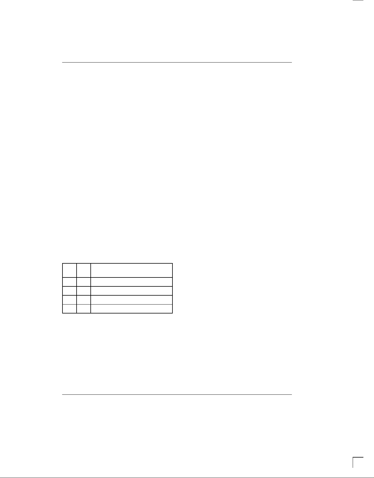
to 5V or a 12V programming pulse. The table below
summarizes these options.
BIT
BIT
4
1
FUNCTION
0 0 strong pull–up to 5V and disarm
1 0 12V Programming Pulse and disarm
0 1 strong pull–up to 5V and arm
1 1 12V Programming Pulse and arm
The strong pull–up to 5V is required to program
EEPROM devices or to operate special function
devices that require a higher current for a limited time
after having received a “go and convert” command.
Therefore and because it significantly reduces the
effective data throughput on the 1–Wire bus, the strong
pull–up is disarmed most of the time. Although arming or
disarming is simultaneously possible while generating a
programming pulse, this is not recommended since it is
PP
likely to destroy the DS2480 if non–EPROM devices are
connected to the 1–Wire bus.
The duration of the strong pull–up or programming
pulse is determined by configuration parameters and
ranges from a few microseconds up to unlimited (see
section Configuration Commands). However, unlimited
duration is not allowed in conjunction with arming the
strong–pull–up after every byte. As long as the DS2480
is in Command Mode the host may terminate a strong
pull–up or programming pulse prematurely at any time
by sending the command code F1h.
The response byte is generated as soon as the strong
pull–up or programming pulse is over (either because
the predefined time has elapsed or due to termination).
The response byte mainly returns the command code
as sent by the host, but the two least significant bits are
undefined.
If the strong pull–up is armed and the device is in Data
Mode, the end of the strong pull–up will be signaled as
code F6h if the most significant bit of the preceding data
byte on the 1–Wire bus was a 1 and 76h otherwise. The
host will see this response byte in addition to the
response on the data byte sent (see also section Wave
Forms later in this document).
SEARCH ACCELERATOR INTRODUCTION
The Search Accelerator is a logic block inside the
DS2480 that allows using the Search ROM function
very efficiently under modern operating systems such
as Windows and Windows 95/NT. Without the DS2480
all 1–Wire port adapters have to involve the computer’s
CPU for every single time slot or pulse to be generated
on the 1–Wire bus.
Under DOS, accessing peripherals such as the UART
or parallel port is very straight forward and therefore
fast. Under Windows the situation is different and it may
take several milliseconds or more to get the first time
slot generated on the 1–Wire bus. Every subsequent
time slot will be generated in much less time, since the
computer simply sends out (“streams”) a long chain of
bytes. This works reasonably well when reading or writing large blocks of data.
042498 7/26
DS2480
Searching the 1–Wire bus to identify all ROM IDs of the
devices connected, however, requires reading two bits,
making a decision and then writing a bit. This procedure
is to be repeated 64 times to identify and address a
single device. With the overhead of modern operating
systems this fairly simple process takes a lot of time,
reducing the discovery rate of devices on the 1–Wire
bus from a typical value of 40 to 50 per second under
DOS to less than 10 under Windows. T o solve this problem the Search Accelerator was developed.
The Search Accelerator receives from the host information on the preferred path to chose during the execution
of the Search ROM function as one contiguous chain of
bytes and then translates it into the appropriate time
slots on the 1–Wire bus. In addition, the Search Accelerator reports back to the host the ROM ID of the device
actually addressed and the bit positions in which conflicts were found. (If the ROM ID of one device has a 0 in
a bit position where another device has a 1, this is called
a “conflict” on the electrical level and “discrepancy” on
the logical level. See the Book of DS19xx i
Button Standards for a more detailed discussion of the Search
ROM). This helps the host to select the preferred path
for the next Search ROM activity.
Since the ROM ID of all MicroLAN compatible devices is
64 bits long and a conflict may occur in any of these bits,
the total length of data reported to the host is 128 bits or
16 bytes. T o avoid data overrun (if the CPU sends data
faster than it can be processed) the protocol for the
Search Accelerator operation was defined so that one
has to send as many bytes as one will receive. This way
the CPU sends 16 bytes for each path and the UART
guarantees the correct data timing and frees the CPU
for other tasks while the DS2480 performs a Search
ROM function.
SEARCH ACCELERATOR OPERATION
After the Search Accelerator is activated and the data
mode is selected, the host must send 16 bytes to complete a single Search ROM pass on the 1–Wire bus.
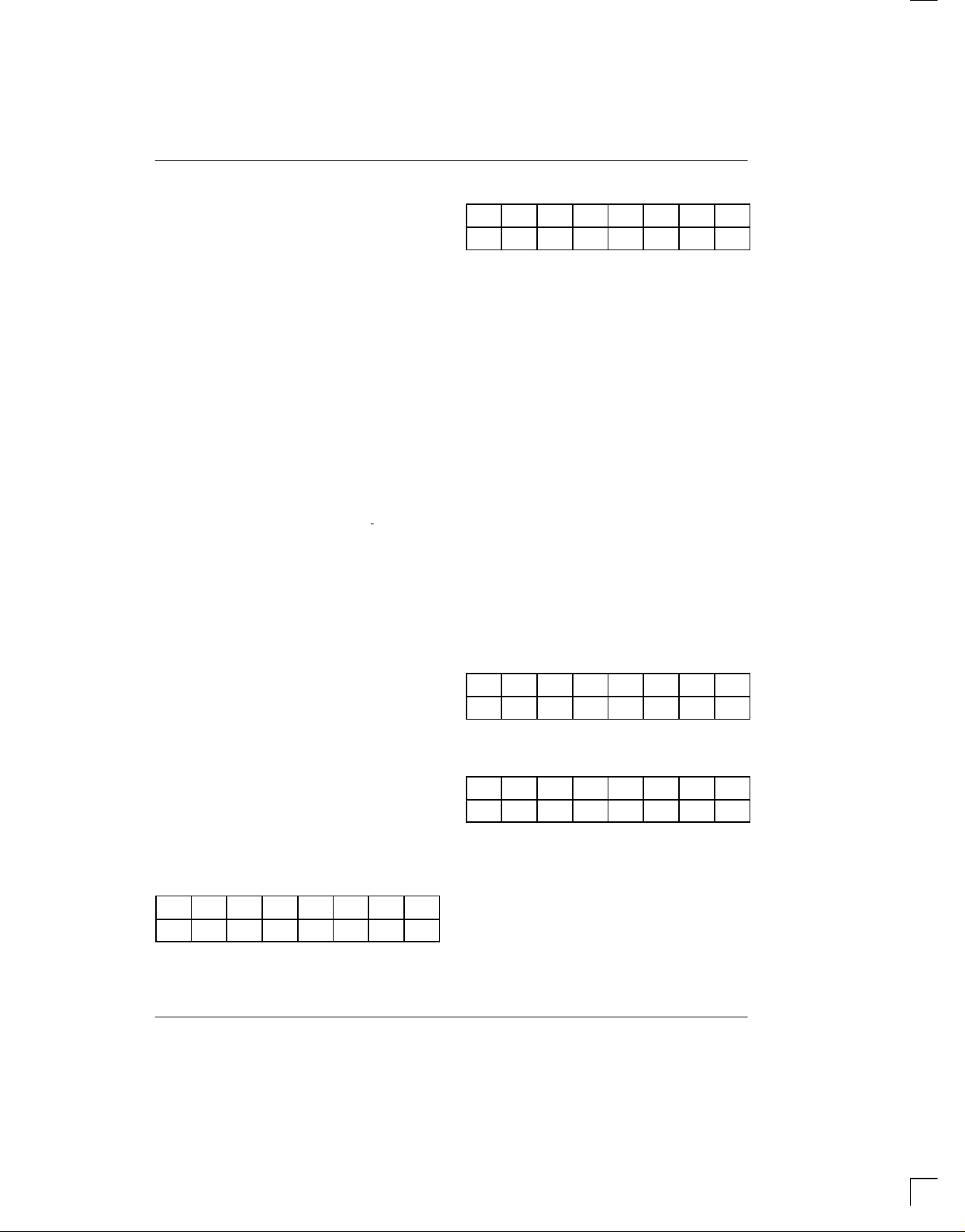
These bytes are constructed as follows:
first byte
7
6 5 4 3 2 1 0
r
3
et cetera
x
3r2
x
2r1
x
1r0
x
0
16th byte
6 5 4 3 2 1 0
7
r
63x63r62x62r61x61r60x60
In this scheme, the index (values from 0 to 63, “n”) designates the position of the bit in the ROM ID of a MicroLAN compatible device. The character “x” marks bits
that act as filler and do not require a specific value (don’t
care bits). The character “r” marks the path to go at that
particular bit in case of a conflict during the execution of
the ROM Search.
For each bit position n (values from 0 to 63) the DS2480
will generate three time slots on the 1–Wire bus. These
are referenced as:
b0 for the first time slot (read data)
b1 for the second time slot (read data) and
b2 for the third time slot (write data).
The type of time slot b2 (write 1 or write 0) is determined
by the DS2480 as follows:
b2 = r
if conflict (as chosen by the host)
n
= b0 if no conflict (there is no alternative)
= 1 if error (there is no response)
The response the host will receive during a complete
pass through a Search ROM function using the Search
Accelerator consists of 16 bytes as follows:
first byte
7
6 5 4 3 2 1 0
r’3d3r’2d2r’1d1r’0d
0
et cetera
16th byte
7
6 5 4 3 2 1 0
r’63d63r’62d62r’61d61r’60d
60
As before, the index (values from 0 to 63, “n”) designates the position of the bit in the ROM ID of a MicroLAN
compatible device. The character “d” marks the discrepancy flag in that particular bit position. The discrepancy
flag will be 1 if there is a conflict or no response in that
particular bit position and 0 otherwise. The character
“r’ ” marks the actually chosen path at that particular bit
position. The chosen path is identical to b2 for the particular bit position of the ROM ID.
042498 8/26
 Loading...