DS2436
Battery ID/Monitor Chip
P
RELIMINARY
www.dalsemi.com
DS2436
GNDDQVDD
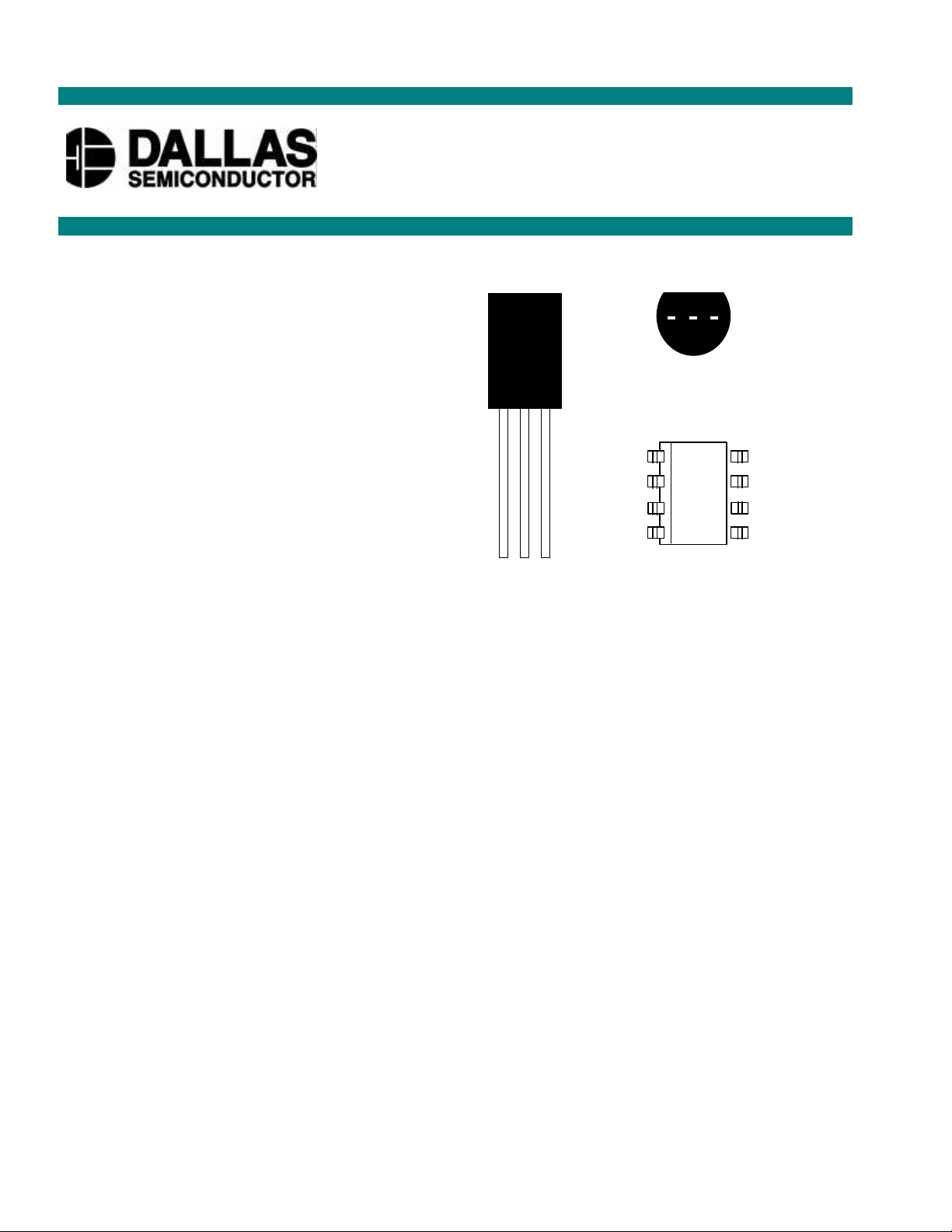
TO-92 PACKAGE
BOTTOM
2
3
DD
NC
NC
NC
NC
NC
DQ
GND
1234876
5
FEATURES
§ Unique 1-Wire™ interface requires only one
port pin for communication
§ Provides unique 64-bit identification number
to battery packs
§ On-board A/D converter monitors battery
voltage for end-of-charge and end-ofdischarge determination
§ Eliminates thermistors by sensing battery
temperature on-chip
§ 256-bit nonvolatile user memory available
for storage of data such as fuel gauge and
manufacturing information
§ 2-byte cycle counter
§ Operating range of -40°C to +85°C
§ Applications include portable computers,
portable/ cellular phones, consumer
electronics, and handheld instrumentation
PACKAGE OUTLINE
DALLAS
DS2436Z
DS2436B
150-mil, 8-Pin SOIC
PIN DESCRIPTION
GND - Ground
DQ - Data In/Out
V
- Supply/Battery Connection
DD
V
DESCRIPTION
The DS2436 Battery Identification/Monitor Chip provides a convenient method of tagging and
identifying battery packs, by manufacturer, chemistry, or other identifying parameters. The DS2436
allows the battery pack to be coded with a unique 64-Bit ROM ID and a 16-Bit Manufacturer ID, and also
store information regarding the battery life and charge/ discharge characteristics in its nonvolatile
memory.
The DS2436 also performs the essential function of monitoring battery temperature, without the need for
a thermistor in the battery pack.
A cycle counter assists to determine the remaining cycle life of the battery.
Finally, the DS2436 measures battery voltage and sends that measured value to a host CPU for use in
end-of-charge or end-of-discharge determination or basic fuel gauge operation.
Information is sent to/from the DS2436 over a 1-Wire interface, so that battery packs need only have
three output connectors: power, ground, and the 1-Wire interface.
1 of 29 092199

DS2436
DETAILED PIN DESCRIPTION
SYMBOL DESCRIPTION
GND
DQ Data input/output pin for 1-Wire communication port
V
DD
NC
Ground pin
Supply Pin- input power supply (battery connection)
No Connect
OVERVIEW
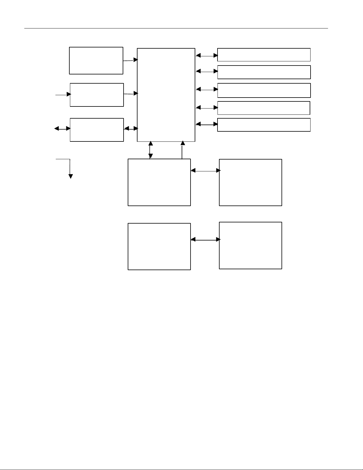
The block diagram of Figure 1 shows the major components of the DS2436. The DS2436 has seven
major data components: 1) 64-bit lasered ROM ID, 2) Scratchpad Memory, 3) Nonvolatile Memory, 4)
On-board SRAM, 5) Temperature sensor, 6) Battery voltage A/D converter, and 7)16-bit Manufacturer
ID Register.
Communication to the DS2436 is via a 1-Wire port. With the 1-Wire port, the memory and control
functions will not be available until the ROM function protocol has been established. The master must
first provide one of four ROM function commands: 1) Read ROM, 2) Match ROM, 3) Search ROM, or 4)
Skip ROM. These commands operate on the 64-bit ROM ID portion of each device and can identify a
specific device if many are present on the 1-Wire line as well as indicate to the bus master how many and
what types of devices are present. After a ROM function sequence has been successfully executed, the
memory and control functions are accessible. The master may then provide any one of the fifteen memory
and control function commands.
Access to the DS2436 memory is through the 1-Wire interface and scratchpad memory. Charging
parameters and other data such as battery chemistry, fuel gauge information, and other user data may be
stored in the DS2436, allowing this information to be permanently stored in the battery pack.
PARASITE POWER
The ID ROM registers and memory of the DS2436 can be read even when the battery is completely
discharged by using parasite-powered operation. When parasite powered, the DS2436 “steals” power
from the DQ line whenever it is high. DQ will provide sufficient power for read operations as long as
specified timing and voltage requirements are met (see the section titled “1-Wire Bus System”).
2 of 29

DS2436 BLOCK DIAGRAM Figure 1
64-BIT ROM ID AND
CONTROL LOGIC AND
256-BIT
64
-BIT
TEMPERA
TU
RE
DS2436
V
DQ
DD
GDD
MEASURING
CIRCUITRY
A/D CONVERTER
1-WIRE PORT
MEMORY FUNCTION
CONTROL
256-BIT SCRATCHPAD
TEMPERATURE REGISTER
STATUS REGISTER
VOLTAGE REGISTER
CYCLE COUNTER
MANUFACTURER ID
NONVOLATILE RAM
64-BIT SCRATCHPAD
RAM
3 of 29

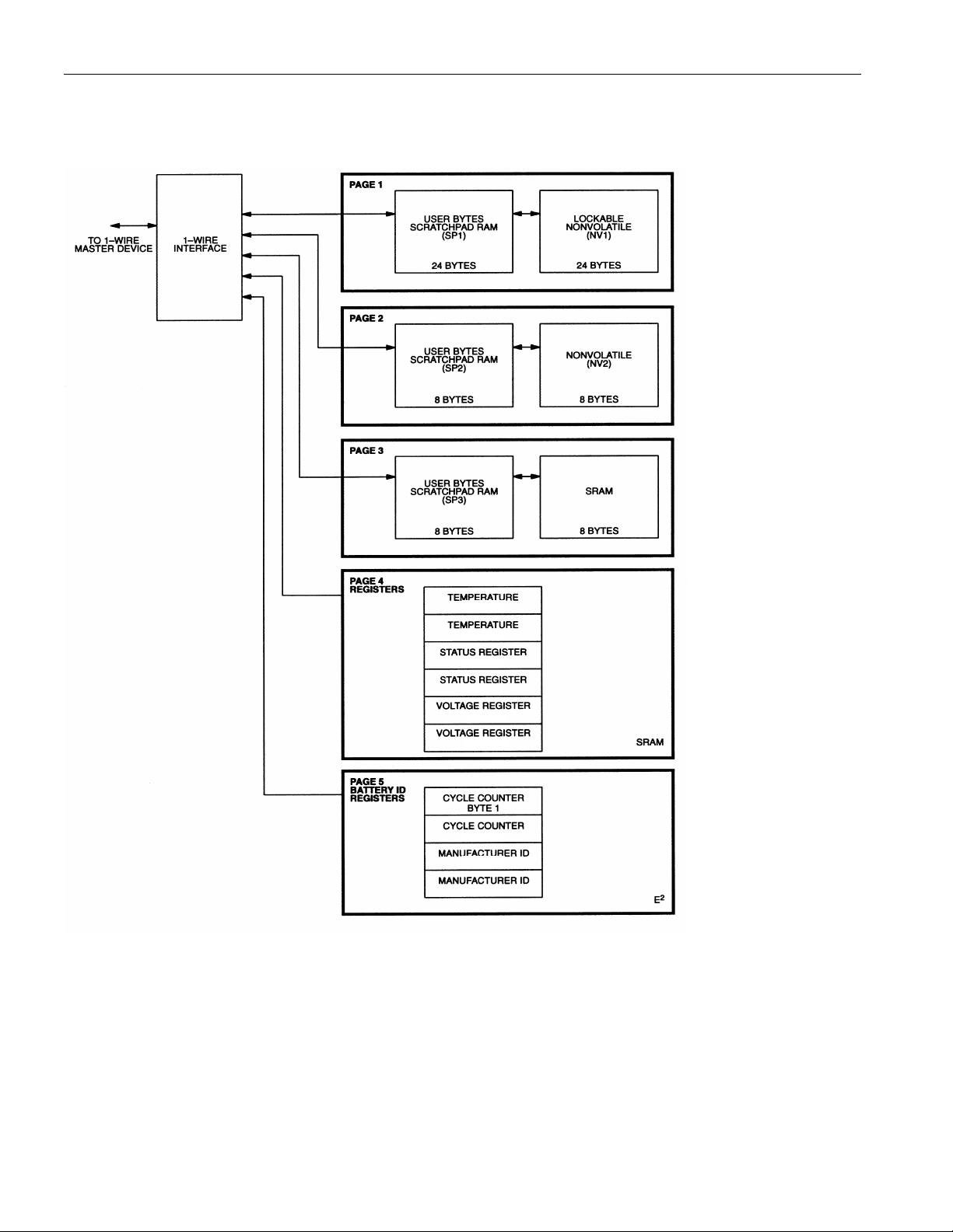
DS2436 MEMORY PARTITIONING Figure 2
LSB
LSB
LSB
LSB
MSB
MSB
MSB
MSB
LSB
MSB
DS2436
4 of 29

DS2436 MEMORY MAP Figure 3
BYTE ADDRESS
PAGE 1 USER BYTE 0 00h
USER BYTE 1 01h
USER BYTE 2 02h
USER BYTE 3 03h
SP1 USER BYTE 4 04h
OR USER BYTE 5 05h
NV1 USER BYTE 6 06h
USER BYTE 7 07h
USER BYTE 8 08h
USER BYTE 9 09h
USER BYTE 10 0Ah
USER BYTE 11 0Bh
USER BYTE 12 0Ch
USER BYTE 13 0Dh
USER BYTE 14 0Eh
USER BYTE 15 0Fh
USER BYTE 16 10h
USER BYTE 17 11h
USER BYTE 18 12h
USER BYTE 19 13h
USER BYTE 20 14h
USER BYTE 21 15h
USER BYTE 22 16h
USER BYTE 23 17h
24 18h
DS2436
RESERVED
ADDRESS
SPACE
31 1Fh
5 of 29

DS2436 MEMORY MAP (cont’d) Figure 3
BYTE ADDRESS
PAGE 2 USER BYTE 0 20h
USER BYTE 1 21h
USER BYTE 2 22h
USER BYTE 3 23h
SP2 USER BYTE 4 24h
OR USER BYTE 5 25h
NV2 USER BYTE 6 26h
USER BYTE 7 27h
8 28h
RESERVED
ADDRESS
SPACE
DS2436
31 3Fh
6 of 29

DS2436 MEMORY MAP (cont’d) Figure 3
BYTE ADDRESS
PAGE 3 USER BYTE 0 40h
USER BYTE 1 41h
USER BYTE 2 42h
USER BYTE 3 43h
SP3 USER BYTE 4 44h
OR USER BYTE 5 45h
SRAM USER BYTE 6 46h
USER BYTE 7 47h
RESERVED
ADDRESS
SPACE
DS2436
31 5Fh
7 of 29

DS2436 MEMORY MAP (cont’d) Figure 3
BYTE ADDRESS
PAGE 4 TEMPERATURE LSB 0 60h
TEMPERATURE MSB 1 61h
STATUS LSB 2 62h
REGISTERS STATUS LSB 3 63h
4 64h
5 65h
6 66h
7 67h
8 68h
9 69h
10 6Ah
11 6Bh
RESERVED
ADDRESS
SPACE
VOLTAGE LSB 23 77h
VOLTAGE MSB 24 78h
12 6Ch
13 6Dh
14 6Eh
15 6Fh
16 70h
17 71h
18 72h
19 73h
20 74h
21 75h
22 76h
DS2436
RESERVED
ADDRESS
SPACE
31 7Fh
8 of 29

DS2436 MEMORY MAP (cont’d) Figure 3
BYTE ADDRESS
PAGE 5 MFG ID LSB 0 80h
MFG ID MSB 1 81h
CYCLE CTR LSB 2 82h
REGISTERS CYCLE CTR LSB 3 83h
RESERVED
ADDRESS
SPACE
DS2436
31 9Fh
9 of 29
 Loading...