Dallas Semiconductor DS2433S-Z01-T-R, DS2433S-Z01, DS2433-Z01-T-R, DS2433-Z01, DS2433X-Z01 Datasheet

1 of 2 030100
FEATURES
4096 bits Electrically Erasable Programmable
Read Only Memory (EEPROM)
Unique, factory-lasered and tested 64-bit
registration number (8-bit family code + 48bit serial number + 8-bit CRC tester) assures
absolute identity because no two parts are
alike
Built-in multidrop controller ensures
compatibility with other MicroLAN products
Memory partitioned into sixteen 256-bit
pages for packetizing data
256-bit scratchpad with strict read/write
protocols ensures integrity of data transfer
Reduces control, address, data and power to a
single data pin
Directly connects to a single port pin of a
microprocessor and communicates at up to
16.3k bits per second
Overdrive mode boosts communication speed
to 142k bits per second
8-bit family code specifies DS2433-Z01
communication requirements to reader
Presence detector acknowledges when reader
first applies voltage
Low cost PR-35, 8-pin SOIC, or solder
bumped flip chip package
Reads and writes over a wide voltage range of
2.8V to 6.0V from -40°C to +85°C
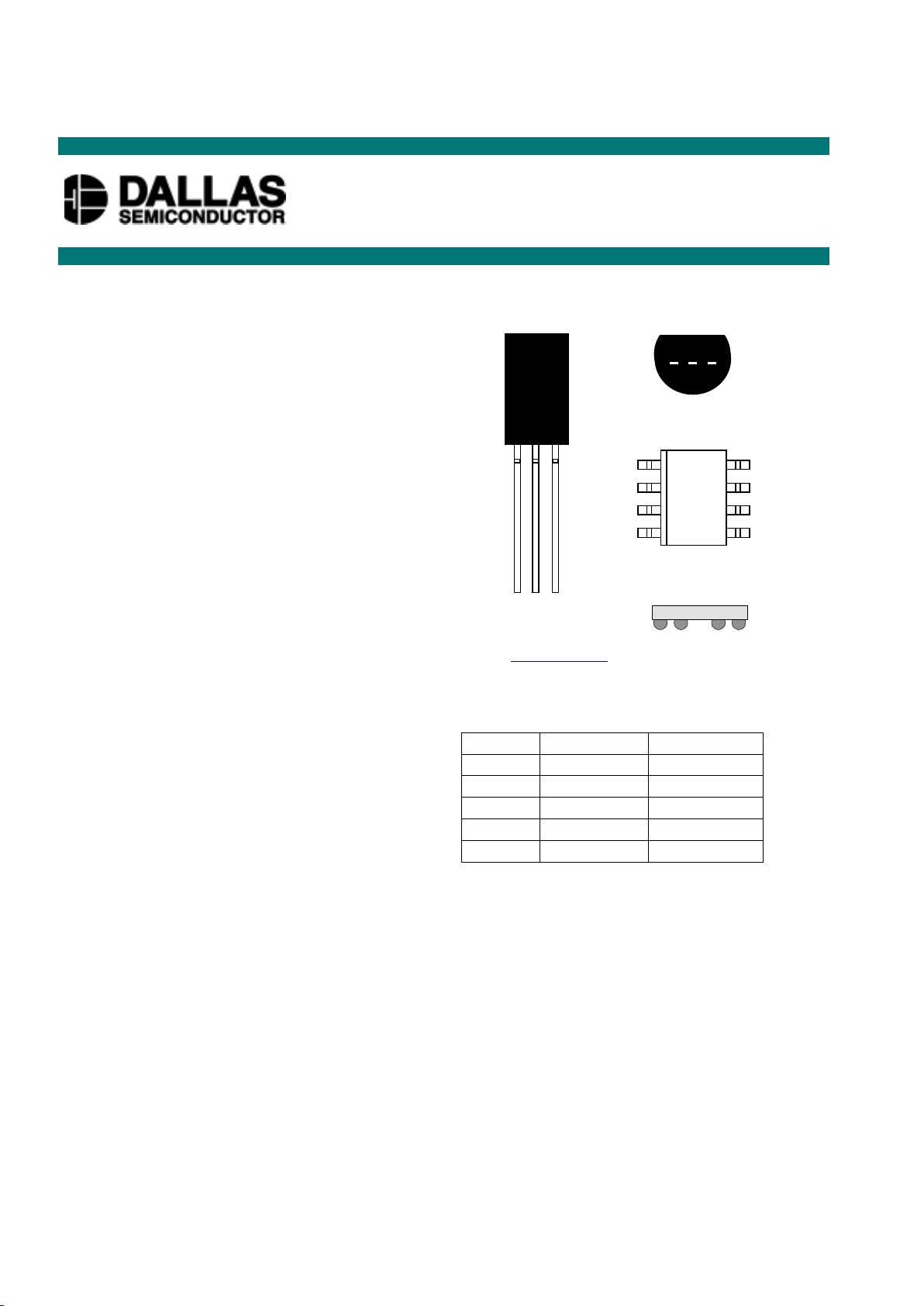
PIN ASSIGNMENT
PIN DESCRIPTION
PR-35 SOIC
Pin 1 Ground NC
Pin 2 Data NC
Pin 3 NC Data
Pin 4 -- Ground
Pin 5-8 -- NC
ORDERING INFORMATION
DS2433-Z01 PR-35 package
DS2433S-Z01 8-pin SOIC package
DS2433T-Z01 Tape & Reel version of DS2433-Z01
DS2433Y-Z01 Tape & Reel version of DS2433S-Z01
DS2433X-Z01 Flip Chip Pkg., Tape & Reel
DESCRIPTION
The DS2433-Z01 is identical to the standard DS2433 with the exception that the write cycle endurance
specification is relaxed to 10,000 cycles as specified in Table 1. The device consists of a factory-lasered
registration number that includes a unique 48-bit serial number, an 8-bit CRC, and an 8-bit Family Code
(23h) plus 4096 bits of user-programmable EEPROM.
DS2433-Z01
4K-Bit 1-WireTM EEPROM
www.dalsemi.com
DATA
GND
NC
NC
2
3
4
8
7
6
5
1
8-PIN SOIC (208 MIL)
123
PR-35
321
BOTTOM VIEW
Flip Chip Package
(Visit www.dalsemi.com for flip chip pinout and mechanical data.)

DS2433-Z01
2 of 2
The power to read and write the DS2433-Z01 is derived entirely from the 1-Wire communication line.
The memory is organized as sixteen pages of 256 bits each. The scratchpad is an additional page that acts
as a buffer when writing to memory. Data is first written to the scratchpad where it may be read back for
verification. A copy scratchpad command will then transfer the data to memory. This process insures
data integrity when modifying the memory. The 64-bit registration number provides a guaranteed unique
identity which allows for absolute traceability and acts as node address if multiple DS2433-Z01 are
connected in parallel to form a local network. Data is transferred serially via the 1-Wire protocol which
requires only a single data lead and a ground return. The PR-35 and SOIC packa ges provide a compact
enclosure that allows standard assembly equipment to handle the device easily for attachment to printed
circuit boards or wiring. Typical applications include storage of calibration constants, board
identification and product revision status.
The DS2433X-Z01 flip chip packaged option is built to the highest quality standards and manufactured
for long term reliability. All Dallas Semiconductor devices are made using the same quality materials
and manufacturing methods. However, standard versions of the DS2433X-Z01 are not exposed to
environmental stresses, such as burn-in, that some industrial applications require. For specific reliability
information on this product please contact Dallas Semiconductor.
Table 1. WRITE CYCLE ENDURANCE SPECIFICATION
Conditions: V
PUP
=5.0V; TA = 25ººººC
PARAMETER SYMBOL MIN TYP MAX UNITS NOTES
Write/Erase Cycles N
CYCLE
10k
Please see the standard DS2433 data sheet for all other device specifications and operational information.
 Loading...