Dallas Semiconductor DS2415V Datasheet

www.dalsemi.com
1-Wire
DS2415
TM
Time Chip
FEATURES
Real Time Clock with fully compatible 1-
Wire MicroLAN interface
Uses the same binary time/date
representation as the DS2404 but with 1
second resolution
Clock accuracy ±2 minutes per month at
25°C
Communicates at 16.3 kbits per second
Unique, factory-lasered and tested 64-bit
registration number (8-bit family code + 48bit serial number + 8-bit CRC tester) assures
absolute traceability because no two parts are
alike
8-bit family code specifies device
communication requirements to bus master
Built-in multidrop controller ensures
compatibility with other MicroLAN products
Operates over a wide VDD voltage range of
2.5V to 5.5V from -40°C to +85°C
Low power, 200 nA typically with oscillator
running
Compact, low cost 6-pin TSOC surface
mount package
PIN ASSIGNMENT
6-Pin TSOC PACKAGE
TOP VIEW
PIN DESCRIPTION
Pin 1 - GND
Pin 2 - 1-Wire
Pin 3 - V
Pin 4 - V
Pin 5 - X1
Pin 6 - X2
DD
BAT
ORDERING INFORMATION
DS2415P 6-pin TSOC package
DS2415V Tape & Reel of DS2415P
DS2415X Chip Scale Pkg., Tape & Reel
DESCRIPTION
The DS2415 1-Wire Time Chip offers a simple solution for storing and retrievin g vital time information
with minimal hardware. The DS2415 contains a unique, lasered ROM and a real time clock/calendar
implemented as a binary counter. Only one pin is required for communication with the devi ce. Utiliz ing a
backup energy source, the data is nonvolatile and allows for st and-alone operation. Th e DS2415 features
can be used to add functions such as calendar, time and date stamp and logbook to any t ype of electronic
device or embedded application that uses a microcontroller.
OVERVIEW
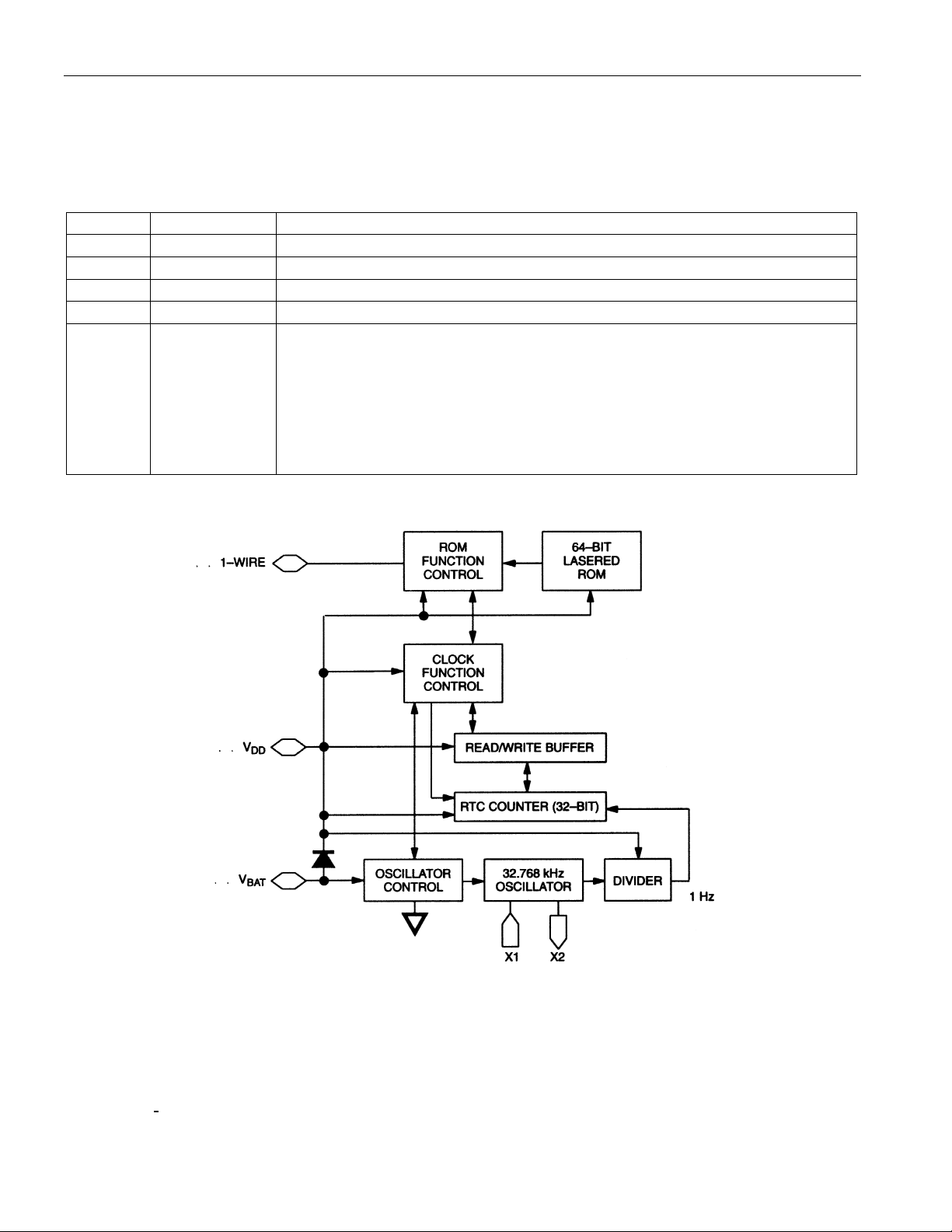
The DS2415 has two main data components: 1) 64-bit lasered ROM, and 2) real time clock counter
(Figure 1). The real time clock utilizes an on-chip oscillator that is connected to an external 32.768 kHz
crystal. All data is read and written least significant bit first. The real time clock functions will not be
available until the ROM function protocol has been established. This protocol is described in the ROM
1 of 14 012200

DS2415
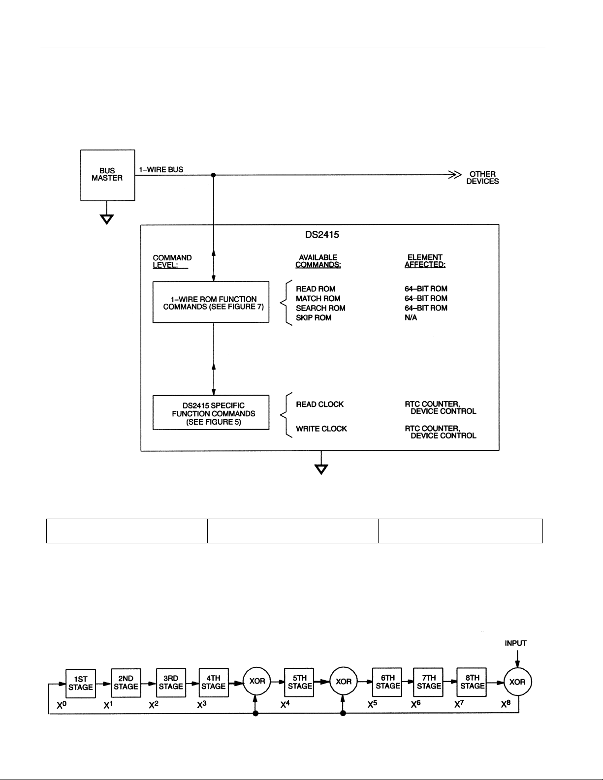
Functions flow chart (Figure 7). The master must first provide one of four ROM function commands: 1)
Read ROM, 2) Match ROM, 3) Search ROM, 4) Skip ROM. After a ROM function sequence has been
successfully executed, the real time clock functions are accessible and the master m a y then provide a re al
time clock function command (Figure 5).
DETAILED PIN DESCRIPTION
PIN SYMBOL DESCRIPTION
1 GND
21-WireData input/output. Open drain.
3VDDInternal power line. Connect a capacitor
4V
5,6 X1,X2
BAT
Ground pin.
Power input pin. 2.5V to 5.5V.
Crystal pins. Connections for a standard 32.768 kHz quartz crystal,
EPSON part number C-002RX or C-004R (be sure to request 6 pF load
capacitance).
NOTE: X1 and X2 are very high-impedance nodes. It is recommended
that they and the crystal be guard-ringed with ground and that high
frequency signals be kept away from the crystal area. See Figure 10 and
Application Note 58 for details.
BLOCK DIAGRAM Figure 1
64-BIT LASERED ROM
Each DS2415 contains a unique ROM code that is 64 bits long. The first 8 bits are a 1-Wire family code.
The next 48 bits are a unique serial number. The last 8 bits are a CRC of the first 56 bits. (See Figure 3.)
The 1-Wire CRC of the lasered ROM is generated using the polynomial X8 + X5 + X4 + 1. Additional
information about the Dallas Semiconductor 1-Wire Cyclic Redundancy Check is available in the Book
of DS19xx iButton Standards. The 64-bit ROM and ROM Function Control section allow the DS2415 to
operate as a 1-Wire device and follow the 1-Wire protocol detailed in the section ”1-Wire Bus S ystem.”
2 of 14

DS2415
The functions required to exercise the control functions of the DS2415 are not accessible until the ROM
function protocol has been satisfied. This protocol is described in the ROM functions flow chart
(Figure 7). The 1-Wire bus master must first provide one of the four ROM function commands. After a
ROM function sequence has been successfully executed, the bus master may then provide one of the
function commands specific to the DS2415 (Figure 5).
HIERARCHICAL STRUCTURE FOR 1-WIRE PROTOCOL Figure 2
64-BIT LASERED ROM Figure 3
MSB LSB
8-Bit CRC Code 48-Bit Serial Number 8-Bit Family Code (24H)
MSB LSB MSB LSB MSB LSB
1-WIRE CRC GENERATOR Figure 4
Polynomial = X8 + X5 + X4 + 1
3 of 14

DS2415
TIMEKEEPING
A 32.768 kHz crystal oscillator is used as the time base for the real time clock counter. The oscillator can
be turned on or off under software control. The oscillator must be on for the real time clock to function.
The real time clock counter is double-buffered. This allows the master to read time without the data
changing while it is being read. To accomplish this, a snapshot of the counter data is transferred to a
read/write buffer, which the user accesses.
DEVICE CONTROL BYTE
The on/off control of the 32.768 kHz crystal oscillator is done through the device control byte. This byte
can be read and written through the Clock Function commands.
Device Control Byte
76543210
U4 U3 U2 U1
Bit 0 - 1 0 No function
Bits 0 and 1 are hard-wired to read all 0s.
Bit 2 - 3 OSC Oscillator Enable/Disable
These bits control/report whether the 32.768 kHz crystal oscillator is running. If the oscillator is running,
both OSC bits will read 1. If the oscillator is turned off these bits will read 0. When writing the device
control byte both occurrences of the OSC bit should have identical data. Otherwise the value in bit
address 3 (bold) takes precedence.
Bit 4 - 7 Un General-purpose user flags
These bits have no particular function within the chip. They can be read and written under the control of
the application software and remain non-volatile as long as there is sufficient voltage at the VDD pin. If
the DS2415 is located inside a battery pack, for example, these bits could convey data on the charging
status from the charging station to the equipment that uses the battery.
OSC
OSC 0 0
Real time Clock
The real time clock is a 32-bit binary counter. It is incremented once per second. The real time clock can
accumulate 136 years of seconds before rolling over. Time/date is represented by the number of seconds
since a reference point, which is determined by the user. For example, 12:00 a.m., January 1, 1970 could
be a reference point.
CLOCK FUNCTION COMMANDS
The “Clock Function Flow Chart” (Figure 5) describes the protocols necessary for accessing the real time
clock. With only 4 bytes of real time clock and one control byte the DS2415 does not provide random
access. Reading and writing always starts with the device control byte followed by the least significant
byte of the time data.
4 of 14

DS2415
READ CLOCK [66h]
The Read Clock command is used to read the device control byte and the contents of the real time clock
counter. After having received the most significant bit of the command code the device copies the actual
contents of the real time clock counter to the read/write buffer. Now the bus master re ads data beginning
with the device control byte followed by the least significant byte through the most significant byte of the
real time clock. After this the bus master may continue reading from the DS2415. The data received will
be the same as in the first pass through the command flow. The Read Clock command can be ended at
any point by issuing a Reset Pulse.
WRITE CLOCK [99h]
The Write Clock command is used to set the real time clock counter and to write the d evice control b yte.
After issuing the command, the bus master writes first the device control byte, which becomes
immediately effective. After this the bus master sends the least significant byte through the most
significant byte to be written to the real time clock counter. The new time data is copied from the
read/write buffer to the real time clock counter and becomes effective as the bus master generates a Reset
Pulse. If the oscillator is intentionally stopped the real time clock counter behaves as a 4-byte nonvolatile memory.
5 of 14
 Loading...