Dallas Semiconductor DS2404-001, DS2404S-C01, DS2404S-001-T-R, DS2404S-001, DS2404B-T-R Datasheet
...
1 of 28 020998
FEATURES
§ 4096 bits of nonvolatile dual-port memory
including real time clock/calendar in binary
format, programmable interval timer, and
programmable power-on cycle counter
§ 1-Wire
TM
interface for MicroLAN
communication at 16.3k bits per second
§ 3-wire host interface for high-speed data
communications at 2M bits per second
§ Unique, factory-lasered and tested 64-bit
registration number (8-bit family code + 48bit serial number + 8-bit CRC tester) assures
absolute traceability because no two parts are
alike
§ Memory partitioned into 16 pages of 256-bits
for packetizing data
§ 256-bit scratchpad with strict read/write
protocols ensures integrity of data transfer
§ Programmable alarms can be set to generate
interrupts for interval timer, real time clock,
and/or cycle counter
§ 16-pin DIP, SOIC and SSOP packages
§ Operating temperature range from -40°C to
+85°C
§ Operating voltage range from 2.8 to 5.5
Volts
ORDERING INFORMATION
DS2404 16-pin DIP
DS2404S 16-pin SOIC
DS2404B 16-pin SSOP
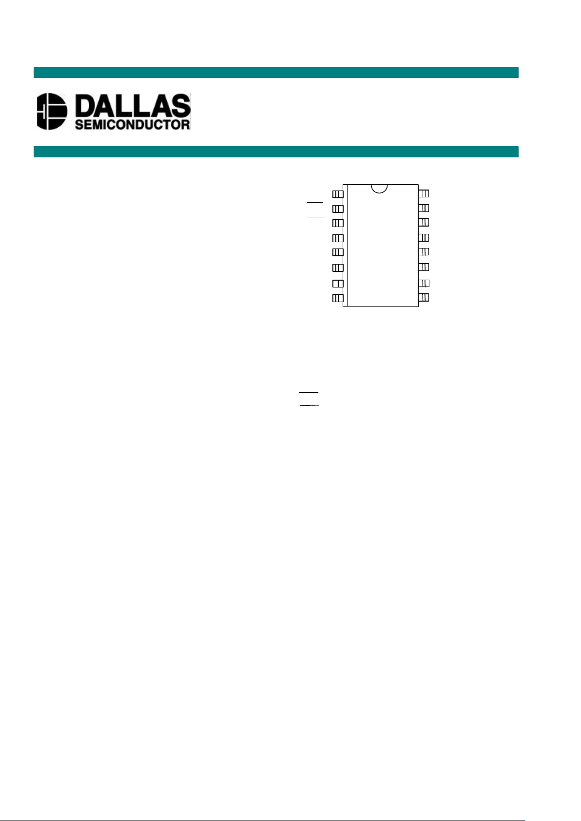
PIN ASSIGNMENT
PIN DESCRIPTION
VCC – 2.8 to 5.5 Volts
IRQ – Interrupt Output
RST – 3-Wire Reset Input
DQ – 3-Wire Input/Output
I/O – 1-Wire Input/Output
CLK – 3-Wire Clock Input
NC – No Connection
GND – Ground
V
BATB
– Battery Backup Input
V
BATO
– Battery Operate Input
1 Hz – 1 Hz Output
X1 ,X2 – Crystal Connections
DESCRIPTION
The DS2404 EconoRAM Time Chip offers a simple solution for storing and retrieving vital data and time
information with minimal hardware. The DS2404 contains a unique lasered ROM, real-time
clock/calendar, interval timer, cycle counter, programmable interrupts and 4096-bits of SRAM. Two
separate ports are provided for communication, 1-Wire and 3-wire. Using the 1-Wire port, only one pin is
required for communication, and the lasered ROM can be read even when the DS2404 is without power.
The 3-wire port provides high speed communication using the traditional Dallas Semiconductor 3-wire
interface. With either interface, a strict protocol for accessing the DS2404 ensures data integrity. Utilizing
backup energy sources, the data is nonvolatile and allows for stand-alone operation.
The DS2404 features can be used to create a stopwatch, alarm clock, time and date stamp, logbook, hour
meter, calendar, system power cycle timer, expiration timer, and event scheduler.
VCC 1 16 VCC
IRQ 2 15 X1
RST 3 14 X2
DQ 4 13 GND
I/O 5 12 NC
CLK 6 11 1HZ
NC 7 10 VBATO
GND 8 9 VBATB
16-PIN DIP (300 MIL)
16-PIN SOIC (300 MIL)
16-PIN SSOP (300 MIL)
See Mechanical Drawings Section
DS2404
EconoRAM Time Chip
www.dalsemi.com

DS2404
2 of 28 020998
DETAILED PIN DESCRIPTION
PIN SYMBOL DESCRIPTION
1,16 V
CC
Power input pins for V
CC
operate mode. 2.8 to 5.5 volts operation.
Either pin can be used for V
CC
. Only one is required for normal
operation. (See V
BATO
pin description and “Power Control” section).
2
IRQ
Interrupt output pin: Open drain.
3
RST
Reset input pin for 3-wire operation. (See “Parasite Power” section.)
4 DQ Data input/output pin for 3-wire operation.
5 I/O Data input/output for 1-Wire operation: Open drain. (See “Parasite
Power” section.)
6 CLK Clock input pin for 3-wire operation.
7,12 NC
No connection pins.
8,13 GND Ground pin: Either pin can be used for ground.
9 V
BATB
Battery backup input pin: Battery voltage can be 2.8 to 5.5 volts.
(See V
BATO
pin description and “Power Control” section.)
10 V
BATO
Battery operate input pin for 2.8 to 5.5 volt operation. The V
CC
&
V
BATB
pins must be grounded when this pin is used to power the chip.
(See “Power Control” section.)
11 1Hz 1 Hz square wave output: Open drain.
14,15 X1,X
2
Crystal pins. Connections for a standard 32.768 kHz quartz crystal,
EPSON part number C-002RX or C-004R (be sure to request 6 pF
load capacitance).
NOTE: X1 and X2 are very high impedance nodes. It is
recommended that they and the crystal be guard-ringed with ground
and that high frequency signals be kept away from the crystal area.
See Figure 18 and Application Note 58 for details.
OVERVIEW
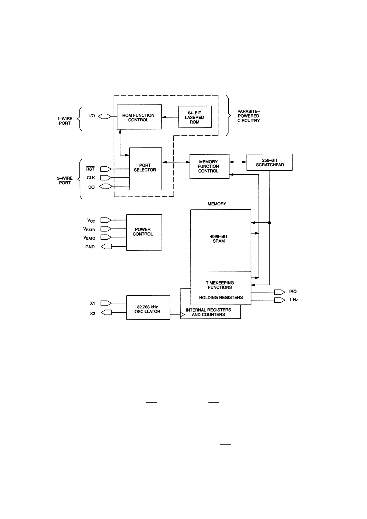
The DS2404 has four main data components: 1) 64-bit lasered ROM, 2) 256-bit scratchpad, 3) 4096-bit
SRAM, and 4) timekeeping registers. The timekeeping section utilizes an on-chip oscillator that is
connected to an external 32.768 kHz crystal. The SRAM and timekeeping registers reside in one
contiguous address space referred to hereafter as memory. All data is read and written least significant bit
first.
Two communication ports are provided, a 1-Wire port and a 3-wire port. A port selector determines
which of the two ports is being used. The communication ports and the ROM are parasite-powered via
I/O, RST , or VCC . This allows the ROM to be read in the absence of power. The ROM data is accessible
only through the 1-Wire port. The scratchpad and memory are accessible via either port.
If the 3-wire port is used, the master provides one of four memory function commands: 1) read memory,
2) read scratchpad, 3) write scratchpad, or 4) copy scratchpad. The only way to write memory is to first
write the scratchpad and then copy the scratchpad data to memory. (See Figure 6.)
If the 1-Wire port is used, the memory functions will not be available until the ROM function protocol
has been established. This protocol is described in the ROM functions flow chart (Figure 9). The master
must first provide one of five ROM function commands: 1) read ROM, 2) match ROM, 3) search ROM,
4) skip ROM or 5) search interrupt. After a ROM function sequence has been successfully executed, the
memory functions are accessible and the master may then provide any one of the four memory function
commands (Figure 6.)
DS2404
3 of 28 020998
The “Power Control” section provides for two basic power configurations, battery operate mode and V
CC
operate mode. The battery operate mode utilizes one supply connected to V
BATO
. The VCC operate mode
may utilize two supplies; the primary supply connects to VCC and a backup supply connects to V
BATB
.
DS2404 BLOCK DIAGRAM Figure 1
COMMUNICATION PORTS
Two communication ports are provided, a 1-Wire and a 3-wire port. The advantages of using the 1-Wire
port are as follows: 1) provides access to the 64-bit lasered ROM, 2) consists of a single communication
signal (I/O), and 3) multiple devices may be connected to the 1-Wire bus. The 1-Wire bus has a
maximum data rate of 16.3k bits/second and requires one 5kΩ external pullup.
The 3-wire port consists of three signals, RST , CLK, and DQ. RST is an enable input, DQ is bidirectional
serial data, and the CLK input is used to clock in or out the serial data. The advantages of using the 3wire port are 1) high data transfer rate (2 MHz), 2) simple timing, and 3) no external pullup required.
Port selection is accomplished on a first-come, first-serve basis. Whichever port comes out of reset first
will obtain control. For the 3-wire port, this is done by bringing RST high. For the 1-Wire port, this is
done on the first falling edge of I/O after the reset and presence pulses. (See “1-Wire Signaling” section.)
DS2404
4 of 28 020998
More information on how to arbitrate port access is found in section “Device Operation Modes” later in
this document.
PARASITE POWER
The block diagram (Figure 1) shows the parasite-powered circuitry. This circuitry “steals” power
whenever the I/O, RST , or VCC pins are high. When using the 1-Wire port in battery operate mode,
RST and V
CC
provide no power since they are low. However, I/O will provide sufficient power as long as
the specified timing and voltage requirements are met. The advantages of parasite power are two-fold: 1)
by parasiting off these pins, battery power is conserved and 2) the ROM may be read in absence of
normal power. For instance, in battery-operate mode, if the battery fails, the ROM may still be read
normally.
In battery-backed mode, if VCC fails, the port switches in the battery but inhibits communication. The
ROM may still be read normally over the 1-Wire port if RST is low.
64-BIT LASERED ROM
Each DS2404 contains a unique ROM code that is 64 bits long. The first eight bits are a 1-Wire family
code (DS2404 code is 04h). The next 48 bits are a unique serial number. The last eight bits are a CRC of
the first 56 bits. (See Figure 2.)
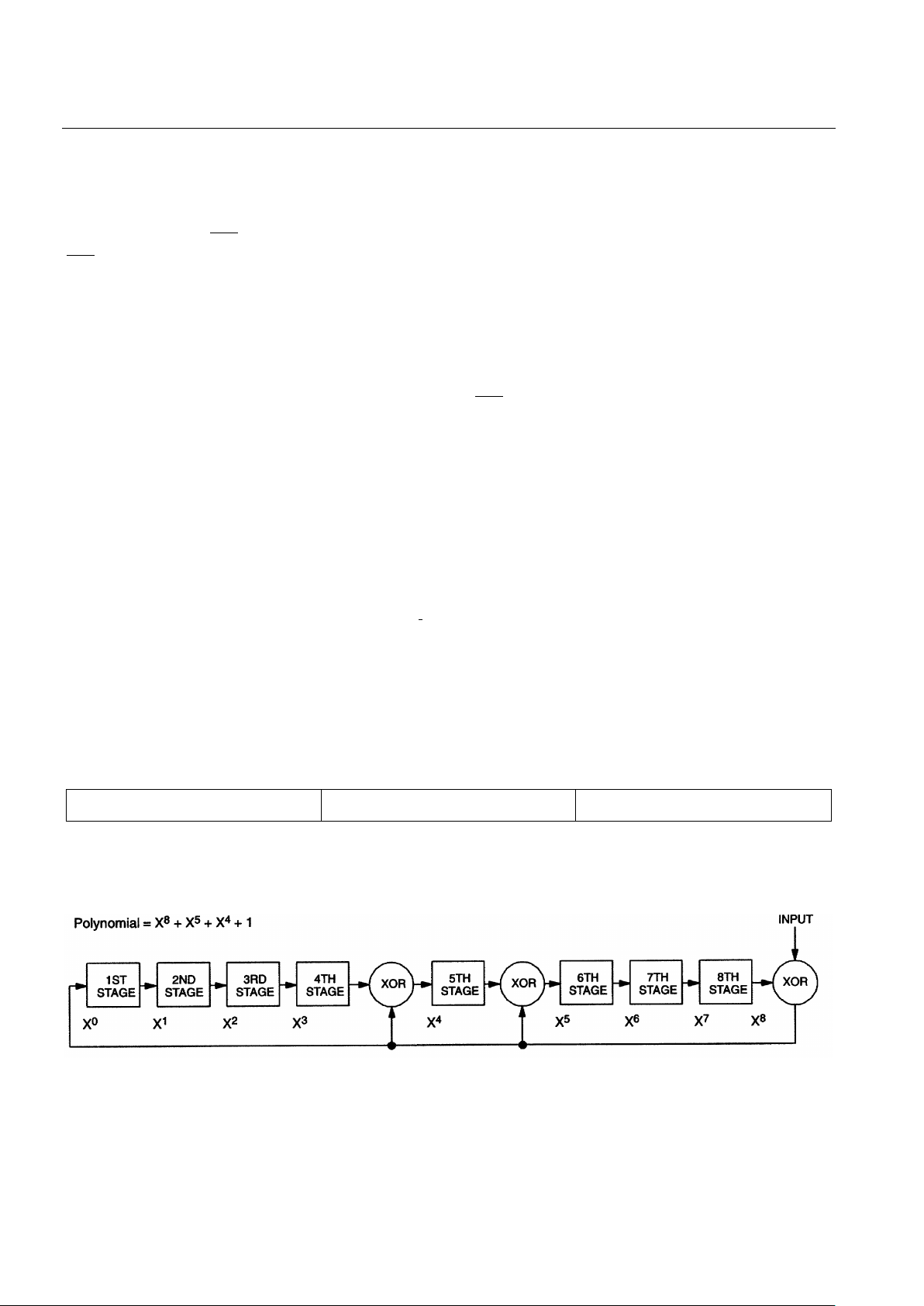
The 1-Wire CRC is generated using a polynomial generator consisting of a shift register and XOR gates
as shown in Figure 3. The polynomial is X8 + X5 + X4 + 1. Additional information about the Dallas 1Wire Cyclic Redundancy Check is available in Application Note 27, “Understanding and Using Cyclic
Redundancy Checks with Dallas Semiconductor iButton Products”.
The shift register bits are initialized to zero. Then starting with the least significant bit of the family code,
one bit at a time is shifted in. After the 8th bit of the family code has been entered, then the serial number
is entered. After the 48th bit of the serial number has been entered, the shift register contains the CRC
value. Shifting in the eight bits of CRC should return the shift register to all zeros.
64-BIT LASERED ROM Figure 2
CRC SERIAL NUMBER DS2404 FAMILY CODE
8-BITS 48-BIT UNQUE NUMBER 04h
MSB LSB
1-WIRE CRC CODE Figure 3
DS2404
5 of 28 020998
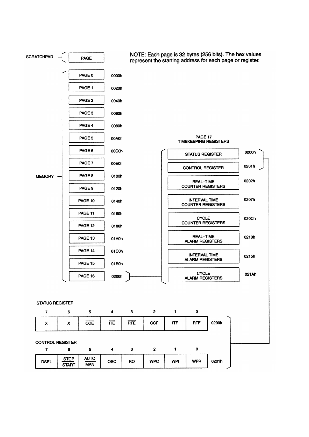
MEMORY MAP Figure 4

DS2404
6 of 28 020998
MEMORY
The memory map in Figure 4 shows a page (32 bytes) called the scratchpad and 17 pages called memory.
Pages 0 through 15 each contain 32 bytes which make up the 4096-bit SRAM. Page 16 has only 30 bytes
which contain the timekeeping registers.
The scratchpad is an additional page of memory that acts as a buffer when writing to memory. Data is
first written to the scratchpad where it can be read back. After the data has been verified, a copy
scratchpad command will transfer the data to memory. This process ensures data integrity when
modifying the memory.
TIMEKEEPING
A 32.768 kHz crystal oscillator is used as the time base for the timekeeping functions. The oscillator can
be turned on or off by an enable bit in the control register. The oscillator must be on for the real time
clock, interval timer, cycle counter and 1 Hz output to function.
The timekeeping functions are double buffered. This feature allows the master to read time or count
without the data changing while it is being read. To accomplish this, a snapshot of the counter data is
transferred to holding registers which the user accesses. This occurs after the eighth bit of the Read
Memory Function command.
Real-Time Clock
The real-time clock is a 5-byte binary counter. It is incremented 256 times per second. The least
significant byte is a count of fractional seconds. The upper four bytes are a count of seconds. The realtime clock can accumulate 136 years of seconds before rolling over. Time/date is represented by the
number of seconds since a reference point which is determined by the user. For example, 12:00A.M.,
January 1, 1970 could be a reference point.
Interval Timer
The interval timer is a 5-byte binary counter. When enabled, it is incremented 256 times per second. The
least significant byte is a count of fractional seconds. The interval timer can accumulate 136 years of
seconds before rolling over. The interval timer has two modes of operation which are selected by the
MANAUTO/ bit in the control register. In the auto mode, the interval timer will begin counting after the
I/O line has been high for a period of time determined by the DSEL bit in the control register. Similarly,
the interval timer will stop counting after the I/O line has been low for a period of time determined by the
DSEL bit. In the manual mode, time accumulation is controlled by the STARTSTOP/ bit in the control
register.
NOTE: For auto mode operation, the high level on the I/O pin must be greater than or equal to 70% of
VCC or V
BATO
.
Cycle Counter
The cycle counter is a 4-byte binary counter. It increments after the falling edge of the I/O line if the
appropriate I/O line timing has been met. This timing is selected by the DSEL bit in the control register.
(See “Status/ Control” section).
NOTE: For cycle counter operation, the high level on the I/O pin must be greater than or equal to 70% of
V
CC
or V
BATO
.
DS2404
7 of 28 020998
Alarm Registers
The alarm registers for the real-time clock, interval timer, and cycle counter all operate in the same
manner. When the value of a given counter equals the value in its associated alarm register, the
appropriate flag bit is set in the status register. If the corresponding interrupt enable bit(s) in the status
register is set, an interrupt is generated. If a counter and its associated alarm register are write protected
when an alarm occurs, access to the device becomes limited. (See “Status/Control”, “Interrupts”, and the
“Programmable Expiration” sections.)
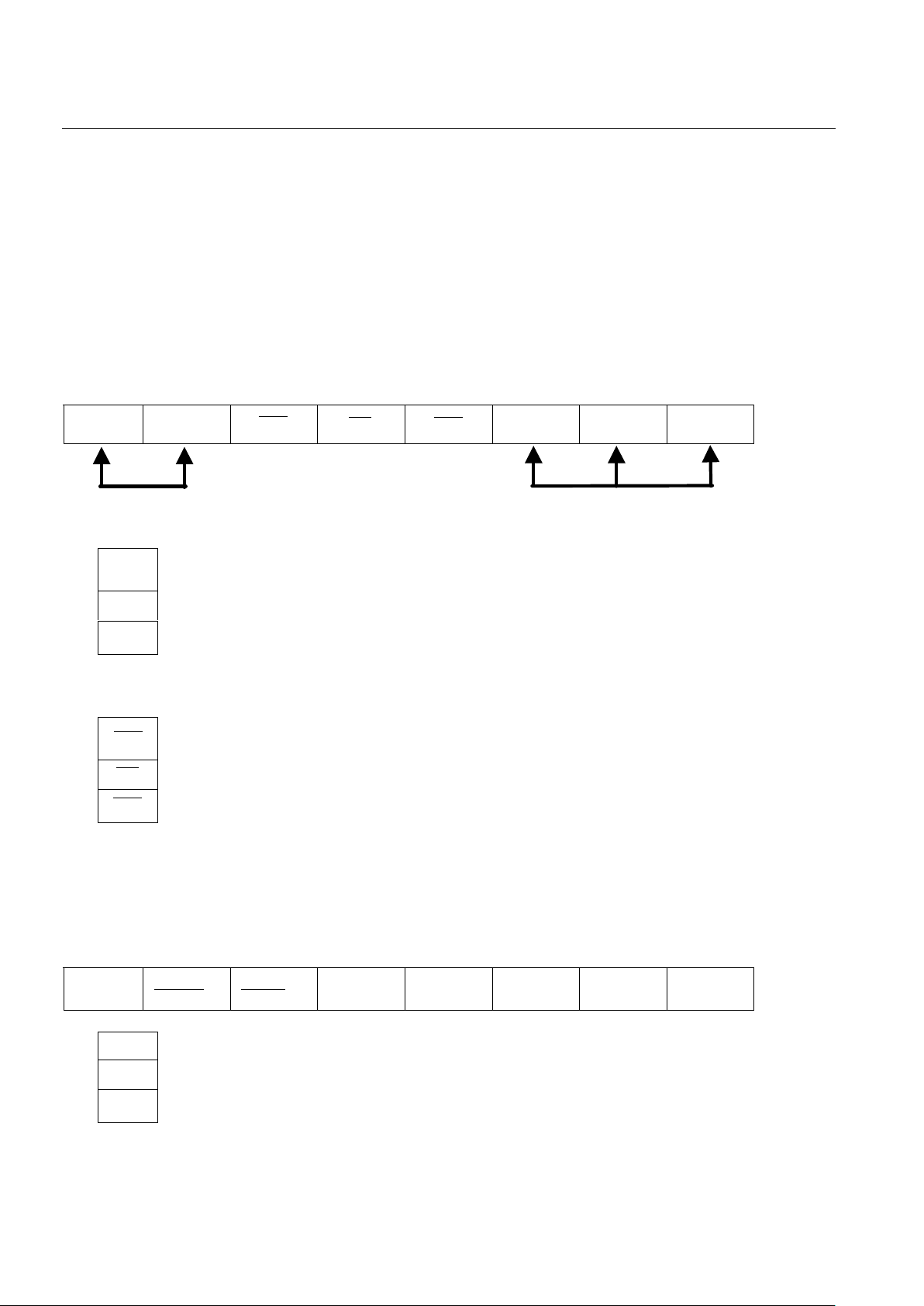
STATUS/CONTROL REGISTERS
The status and control registers are the first two bytes of page 16 (see “Memory Map”, Figure 4).
Status Register
7 6 5 4 3 2 1 0
X X
CCE
ITE
RTE
CCF ITF RTF 0200h
0
RTF Real-time clock alarm flag
1
ITF Interval timer alarm flag
2
CCF Cycle counter alarm flag
When a given alarm occurs, the corresponding alarm flag is set to a logic 1. The alarm flag(s) is cleared
by reading the status register.
3
RTE
Real-time interrupt enable
4
ITE
Interval timer interrupt enable
5 CCE
Cycle counter interrupt enable
Writing any of the interrupt enable bits to a logic 0 will allow an interrupt condition to be generated when
its corresponding alarm flag is set (see “Interrupts” section).
Control Register
7 6 5 4 3 2 1 0
DSEL
START
STOP
MAN.
AUTO
OSC RO WPC WPI WPR 0201h
0
WPR Write protect real-time clock/alarm registers
1
WPI Write protect interval timer/alarm registers
2
WPC Write protect cycle counter/alarm registers
Don’t care bits Read Only

DS2404
8 of 28 020998
Setting a write protect bit to a logic 1 will permanently write protect the corresponding counter and alarm
registers, all write protect bits, and additional bits in the control register. The write protect bits can not be
written in a normal manner (see “Write Protect/Programmable Expiration” section).
3
RO Read Only
If a programmable expiration occurs and the read only bit is set to a logic 1, then the DS2404 becomes
read only. If a programmable expiration occurs and the read only bit is a logic 0, then only the 64-bit
lasered ROM can be accessed (see “Write Protect/Programmable Expiration” section).
4
OSC Oscillator enable
This bit controls the crystal oscillator. When set to a logic 1, the oscillator will start operation. When the
oscillator bit is a logic 0, the oscillator will stop.
5 AUTO/ MAN Automatic/Manual Mode
When this bit is set to a logic 1, the interval timer is in automatic mode. In this mode, the interval timer is
enabled by the I/O line. When this bit is set to a logic 0, the interval timer is in manual mode. In this
mode the interval timer is enabled by the STOP/START bit.
6 STOP/START
Stop/Start (in Manual Mode)
If the interval timer is in manual mode, the interval timer will start counting when this bit is set to a logic
0 and will stop counting when set to a logic 1. If the interval timer is in automatic mode, this bit has no
effect.
7
DSEL Delay Select Bit
This bit selects the delay that it takes for the cycle counter and the interval timer (in auto mode) to see a
transition on the I/O line. When this bit is set to a logic 1, the delay time is 123 + 2 ms. This delay allows
communication on the I/O line without starting or stopping the interval timer and without incrementing
the cycle counter. When this bit is set to a logic 0, the delay time is 3.5 ±0.5 ms.
MEMORY FUNCTION COMMANDS
The “Memory Function Flow Chart” (Figure 6) describes the protocols necessary for accessing the
memory. Two examples follow the flowchart. Three address registers are provided as shown in Figure 5.
The first two registers represent a 16-bit target address (TA1, TA2). The third register is the ending
offset/data status byte (E/S).
The target address points to a unique byte location in memory. The first five bits of the target address
(T4:T0) represent the byte offset within a page. This byte offset points to one of 32 possible byte
locations within a given page. For instance, 00000b points to the first byte of a page where as 11111b
would point to the last byte of a page.

DS2404
9 of 28 020998
The third register (E/S) is a read only register. The first five bits (E4: E0) of this register are called the
ending offset. The ending offset is a byte offset within a page. Bit 5 (PF) is the partial byte flag. Bit 6
(OF) is the overflow flag. Bit 7 (AA) is the authorization accepted flag.
ADDRESS REGISTERS Figure 5
7 6 5 4 3 2 1 0
TARGET ADDRESS (TA1) T7 T6 T5 T4 T3 T2 T1 T0
TARGET ADDRESS (TA2) T15 T14 T13 T12 T11 T10 T9 T8
ENDING ADDRESS WITH
DATA STATUS (E/S)
(READ ONLY)
AA OF PF E4 E3 E2 E1 E0
Write Scratchpad Command [0Fh]
After issuing the write scratchpad command, the user must first provide the 2–byte target address,
followed by the data to be written to the scratchpad. The data will be written to the scratchpad starting at
the byte offset (T4:T0). The ending offset (E4: E0) will be the byte offset at which the host stops writing
data. The maximum ending offset is 11111b (31d). If the host attempts to write data past this maximum
offset, the overflow flag (OF) will be set and the remaining data will be ignored. If the user writes an
incomplete byte and an overflow has not occurred, the partial byte flag (PF) will be set.
Read Scratchpad Command [AAh]
This command may be used to verify scratchpad data and target address. After issuing the read scratchpad
command, the user may begin reading. The first two bytes will be the target address. The next byte will
be the ending offset/data status byte (E/S) followed by the scratchpad data beginning at the byte offset
(T4: T0). The user may read data until the end of the scratchpad after which the data read will be all logic
1’s.
Copy Scratchpad [55h]
This command is used to copy data from the scratchpad to memory. After issuing the copy scratchpad
command, the user must provide a 3-byte authorization pattern. This pattern must exactly match the data
contained in the three address registers (TA1, TA2, E/S, in that order). If the pattern matches, the AA
(Authorization Accepted) flag will be set and the copy will begin. At this point, the part will go into a T
X
mode, transmitting a logic 1 to indicate the copy is in progress. A logic 0 will be transmitted after the data
has been copied. Any attempt to reset the part will be ignored while the copy is in progress. Copy
typically takes 30 µs.
The data to be copied is determined by the three address registers. The scratchpad data from the
beginning offset through the ending offset, will be copied to memory, starting at the target address.
Anywhere from 1 to 32 bytes may be copied to memory with this command. Whole bytes are copied even
if only partially written. The AA flag will be cleared only by executing a write scratchpad command.
 Loading...