Dallas Semiconductor DS21Q44TN, DS21Q44T Datasheet

www.dalsemi.com
DS21Q44
Enhanced QUAD E1 FRAMER
FEATURES
Four E1 (CEPT or PCM-30) /ISDN-PRI
framing transceivers
All four framers are fully independent;
transmit and receive sections of each framer
are fully independent
Frames to FAS, CAS, CCS, and CRC4 formats
Each of the four framers contain dual two–
frame elastic store slip buffers that can
connect to asynchronous backplanes up to
8.192 MHz
8–bit parallel control port that can be used
directly on either multiplexed or non–
multiplexed buses (Intel or Motorola)
Easy access to Si and Sa bits
Extracts and inserts CAS signaling
Large counters for bipolar and code
violations, CRC4 code word errors, FAS
word errors, and E-bits
Programmable output clocks for Fractional
E1, per channel loopback, H0 and H12
applications
Integral HDLC controller with 64-byte buffers
configurable for Sa bits or DS0 operation
Detects and generates AIS, remote alarm,
and remote multiframe alarms
Pin compatible with DS21Q42 Enhanced
Quad T1 Framer
3.3V supply with 5V tolerant I/O; low power
CMOS
Available in 128–pin TQFP package
IEEE 1149.1 support
FUNCTIONAL DIAGRAM
Receive
Framer
Transmit
Formatter
FRAMER #0
FRAMER #1
FRAMER #2
FRAMER #3
Co ntro l Port
Elastic
Store
Elastic
Store
ACTUAL SIZE
QUAD
E1
FRAMER
ORDERING INFORMATION
DS21Q44T (00 C to 700 C)
DS21Q44TN (-400 C to +850 C)
DESCRIPTION
The DS21Q44 E1 is an enhanced version of the DS21Q43 Quad E1 Framer. The DS21Q44 contains four
framers that are configured and read through a common microprocessor compatible parallel port. Each
framer consists of a receive framer, receive elastic stor e, transmit formatter and transmit elastic store. All
four framers in the DS21Q44 are totally independent, they do not share a common fr aming synchronizer.
Also the transmit and receive sides of each framer are totally independent. The dual two-frame elastic
stores contained in each of the four framers can be independently enabled and disabled as required. The
device fully meets all of the latest E1 specifications including CCITT/ITU G.704, G.706, G.962, and
I.431 as well as ETS 300 011 and ETS 300 233.
1 of 105 031600

DS21Q44
1. INTRODUCTION
The DS21Q44 is a superset version of the popular DS21Q43 Quad E1 framer offering the new features
listed below. All of the original features of the DS21Q43 have been retained and software created for the
original device is transferable to the DS21Q44.
New Features
Additional hardware signaling capability including:
– receive signaling reinsertion to a backplane multiframe sync
– availability of signaling in a separate PCM data stream
– signaling freezing
– interrupt generated on change of signaling data
Per–channel code insertion in both transmit and receive paths
Full HDLC controller with 64–byte buffers in both transmit and receive paths. Configurable for Sa
bits or DS0 access
RCL, RLOS, RRA, and RUA1 alarms now interrupt on change of state
8.192 MHz clock synthesizer
Ability to monitor one DS0 channel in both the transmit and receive paths
Option to extend carrier loss criteria to a 1 ms period as per ETS 300 233
Automatic RAI generation to ETS 300 011 specifications
IEEE 1149.1 support
Functional Description
The receive side in each framer locates FAS frame and CRC and CAS multiframe boundaries as well as
detects incoming alarms including, carrier loss, loss of synchronization, AIS and Remote Alarm. If
needed, the receive side elastic store can be enabled in order to absorb the phase and frequency
differences between the recovered E1 data stream and an asynchronous backplane clock which is
provided at the RSYSCLK input. The clock applied at the RSYSCLK input can be either a 2.048 MHz
clock or a 1.544 MHz clock. The RSYSCLK can be a burst clock with speeds up to 8.192 MHz.
The transmit side in each framer is totally independent from the receive side in both the clock
requirements and characteristics. Data off of a backplane can be passed through a transmit side elastic
store if necessary. The transmit formatter will provide the necessary frame/multiframe data overhead for
E1 transmission.
Reader’s Note:
This data sheet assumes a particular nomenclature of the E1 operating environment. In each 125 us frame,
there are 32 eight–bit timeslots numbered 0 to 31. Timeslot 0 is transmitted first and received first. Thes e
32 timeslots are also referred to as channels with a numbering scheme of 1 to 32. Timeslot 0 is identical
to channel 1, timeslot 1 is identical to Channel 2, and so on. Each timeslot (or channel) is made up of
eight bits which are numbered 1 to 8. Bit number 1 is the MSB and is transmitted first. Bit number 8 is
the LSB and is transmitted last. Throughout this data sheet, the following abbreviations will be used:
FAS Frame Alignment Signal CRC4 Cyclical Redundancy Check
CAS Channel Associated Signaling CCS Common Channel Signaling
MF Multiframe Sa Additional bits
Si International bits E-bit CRC4 Error Bits
2 of 105
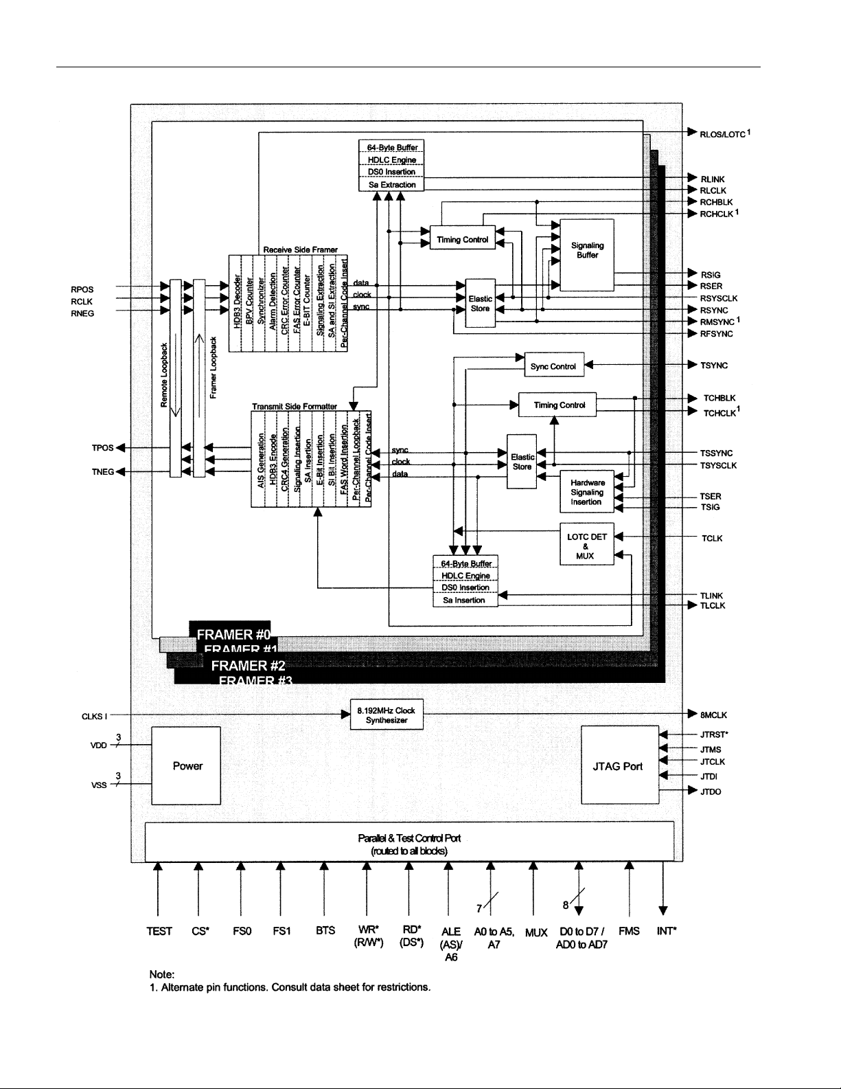
DS21Q44 ENHANCED QUAD E1 FRAMER Figure 1-1
DS21Q44
3 of 105

DS21Q44
TABLE OF CONTENTS
1. INTRODUCTION .............................................................................................................................. 2
2. DS21Q44 PIN DESCRIPTION ......................................................................................................... 7
3. DS21Q44 PIN FUNCTION DESCRIPTION ................................................................................ 13
4. DS21Q44 REGISTER MAP............................................................................................................. 20
5. PARALLEL PORT........................................................................................................................... 24
6. CONTROL, ID AND TEST REGISTERS..................................................................................... 24
7. STATUS AND INFORMATION REGISTERS............................................................................. 34
8. ERROR COUNT REGISTERS....................................................................................................... 40
9. DS0 MONITORING FUNCTION................................................................................................... 43
10. SIGNALING OPERATION ............................................................................................................45
10.1 PROCESSOR BASED SIGNALING........................................................................................ 45
10.2 HARDWARE BASED SIGNALING........................................................................................ 48
11. PER–CHANNEL CODE GENERATION AND LOOPBACK ...................................................49
11.1 TRANSMIT SIDE CODE GENERATION............................................................................... 49
11.1.1 Simple Idle Code Insertion and Per-Channel Loopback................................................... 49
11.1.2 Per-Channel Code Insertion.............................................................................................. 50
11.2 RECEIVE SIDE CODE GENERATION.................................................................................. 51
12. CLOCK BLOCKING REGISTERS............................................................................................... 52
13. ELASTIC STORES OPERATION ................................................................................................ 53
13.1 RECEIVE SIDE......................................................................................................................... 54
13.2 TRANSMIT SIDE ..................................................................................................................... 54
14. ADDITIONAL (SA) AND INTERNATIONAL (SI) BIT OPERATION.................................... 54
14.1 HARDWARE SCHEME ........................................................................................................... 54
14.2 INTERNAL REGISTER SCHEME BASED ON DOUBLE-FRAME..................................... 55
14.3 INTERNAL REGISTER SCHEME BASED ON CRC4 MULTIFRAME............................... 57
4 of 105

DS21Q44
15. HDLC CONTROLLER FOR THE SA BITS OR DS0................................................................. 59
15.1 GENERAL OVERVIEW........................................................................................................... 59
15.2 HDLC STATUS REGISTERS .................................................................................................. 60
15.3 BASIC OPERATION DETAILS............................................................................................... 61
15.4 HDLC REGISTER DESCRIPTION.......................................................................................... 62
16. INTERLEAVED PCM BUS OPERATION................................................................................... 69
17. JTAG-BOUNDARY SCAN ARCHITECTURE AND TEST ACCESS PORT.......................... 72
17.1 DESCRIPTION.......................................................................................................................... 72
17.2 TAP CONTROLLER STATE MACHINE................................................................................ 73
17.3 INSTRUCTION REGISTER AND INSTRUCTIONS ............................................................. 75
17.4 TEST REGISTERS.................................................................................................................... 77
18. TIMING DIAGRAMS...................................................................................................................... 82
19. OPERATING PARAMETERS ...................................................................................................... 92
20. 128-PIN TQFP PACKAGE SPECIFICATIONS ........................................................................ 105
5 of 105

DOCUMENT REVISION HISTORY
Revision Notes
12-22-98 Initial Release
DS21Q44
6 of 105
DS21Q44
2. DS21Q44 PIN DESCRIPTION
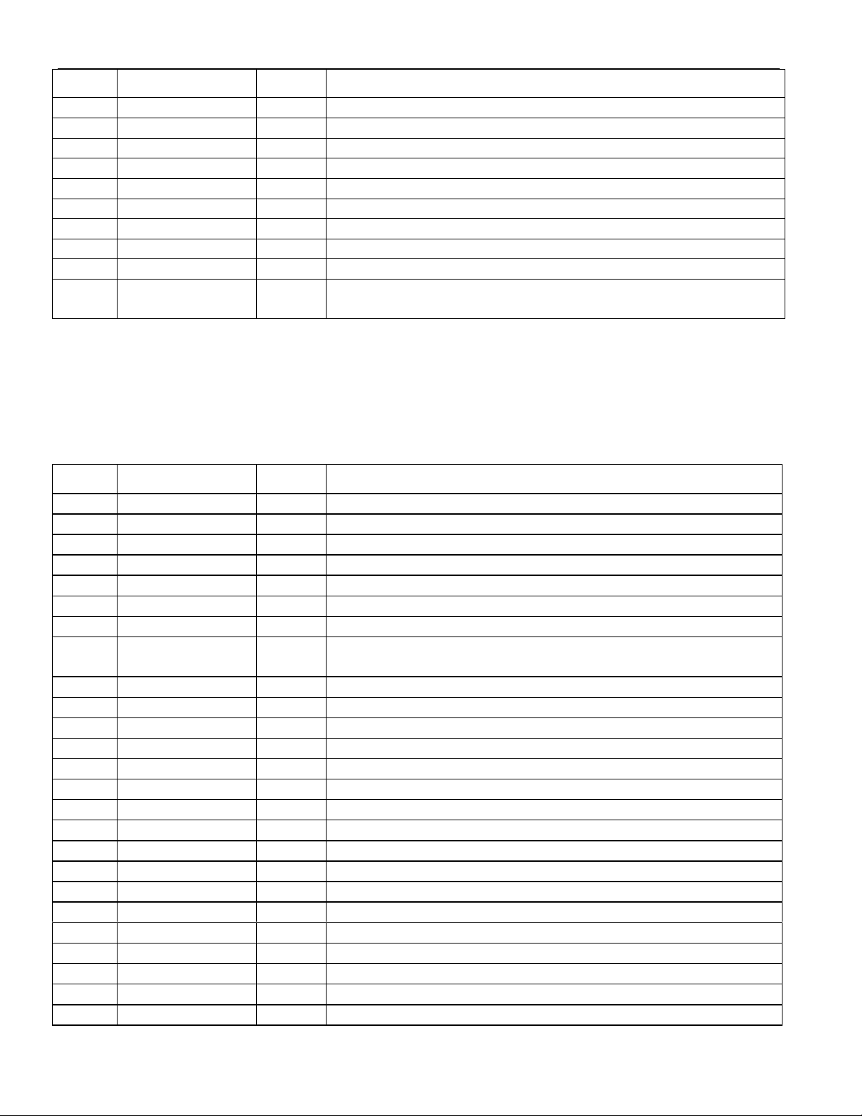
Pin Description Sorted by Pin Number Table 2-1
PIN SYMBOL TYPE DESCRIPTION
1 TCHBLK0 O Transmit Channel Block from Framer 0
2 TPOS0 O Transmit Bipolar Data from Framer 0
3 TNEG0 O Transmit Bipolar Data from Framer 0
4 RLINK0 O Receive Link Data from Framer 0
5 RLCLK0 O Receive Link Clock from Framer 0
6 RCLK0 I Receive Clock for Framer 0
7 RNEG0 I Receive Bipolar Data for Framer 0
8 RPOS0 I Receive Bipolar Data for Framer 0
9RSIG0
[RCHCLK0]
10 RCHBLK0 O Receive Channel Block from Framer 0
11 RSYSCLK0 I Receive System Clock for Elastic Store in Framer 0
12 RSYNC0 I/O Receive Sync for Framer 0
13 RSER0 O Receive Serial Data from Framer 0
14 VSS - Signal Ground
15 VDD - Positive Supply Voltage
16 SPARE1
[RMSYNC0]
17 RFSYNC0 O Receive Frame Sync from Framer 0
18 JTRST*
[RLOS/LOTC0]
19 TCLK0 I Transmit Clock for Framer 0
20 TLCLK0 O Transmit Link Clock from Framer 0
21 TSYNC0 I/O Transmit Sync for Framer 0
22 TLINK0 I Transmit Link Data for Framer 0
23 A0 I Address Bus Bit 0; LSB
24 A1 I Address Bus Bit 1
25 A2 I Address Bus Bit 2
26 A3 I Address Bus Bit 3
27 A4 I Address Bus Bit 4
28 A5 I Address Bus Bit 5
29 A6/ALE (AS) I Address Bus Bit 6; MSB or Address Latch Enable (Address
30 INT* O Receive Alarm Interrupt for all Four Framers
31 TSYSCLK1 I Transmit System Clock for Elastic Store in Framer 1
32 TSER1 I Transmit Serial Data for Framer 1
33 TSSYNC1 I Transmit Sync for Elastic Store in Framer 1
34 TSIG1
[TCHCLK1]
35 TCHBLK1 O Transmit Channel Block from Framer 1
36 TPOS1 O Transmit Bipolar Data from Framer 1
37 TNEG1 O Transmit Bipolar Data from Framer 1
O
[O]
-
[O]
I
[O]
I
[O]
Receive Signaling Output from Framer 0
[Receive Channel Clock from Framer 0]
RESERVED - must be left unconnected for normal operation
[Receive Multiframe Sync from Framer 0]
JTAG Reset
[Receive Loss of Sync/Loss of Transmit clock from Framer 0]
Strobe)
Transmit Signaling Input for Framer 1
[Transmit Channel Clock from Framer 1]
7 of 105
PIN SYMBOL TYPE DESCRIPTION
38 RLINK1 O Receive Link Data from Framer 1
39 RLCLK1 O Receive Link Clock from Framer 1
40 RCLK1 I Receive Clock for Framer 1
41 RNEG1 I Receive Bipolar Data for Framer 1
42 RPOS1 I Receive Bipolar Data for Framer 1
43 RSIG1
[RCHCLK1]
O
[O]
Receive Signaling output from Framer 1
[Receive Channel Clock from Framer 1]
44 RCHBLK1 O Receive Channel Block from Framer 1
45 RSYSCLK1 I Receive System Clock for Elastic Store in Framer 1
46 A7 I Address Bus Bit 7
47 FMS I Framer Mode Select
48 RSYNC1 I/O Receive Sync for Framer 1
49 RSER1 O Receive Serial Data from Framer 1
50 JTMS
[RMSYNC1]
I
[O]
JTAG Test Mode Select
[Receive Multiframe Sync from Framer 1]
51 RFSYNC1 O Receive Frame Sync from Framer 1
52 JTCLK
[RLOS/LOTC1]
I
[O]
JTAG Test Clock
[Receive Loss of Sync/Loss of Transmit clock from Framer 1]
53 TCLK1 I Transmit Clock for Framer 1
54 TLCLK1 O Transmit Link Clock from Framer 1
55 TSYNC1 I/O Transmit Sync for Framer 1
56 TLINK1 I Transmit Link Data for Framer 1
57 TEST I 3-state Control for all Output and I/O Pins
58 FS0 I Framer Select 0 for Parallel Control Port
59 FS1 I Framer Select 1 for Parallel Control Port
60 CS* I Chip Select
61 BTS I Bus Type Select for Parallel Control Port
62 RD*/(DS*) I Read Input (Data Strobe)
63 WR*/(R/W*) I Write Input (Read/Write)
64 MUX I Non-Multiplexed or Multiplexed Bus Select
65 TSYSCLK2 I Transmit System Clock for Elastic Store in Framer 2
66 TSER2 I Transmit Serial Data for Framer 2
67 TSSYNC2 I Transmit Sync for Elastic Store in Framer 2
68 TSIG2
[TCHCLK2]
I
[O]
Transmit Signaling Input for Framer 2
[Transmit Channel Clock from Framer 2]
69 TCHBLK2 O Transmit Channel Block from Framer 2
70 TPOS2 O Transmit Bipolar Data from Framer 2
71 TNEG2 O Transmit Bipolar Data from Framer 2
72 RLINK2 O Receive Link Data from Framer 2
73 RLCLK2 O Receive Link Clock from Framer 2
74 RCLK2 I Receive Clock for Framer 2
75 RNEG2 I Receive Bipolar Data for Framer 2
76 RPOS2 I Receive Bipolar Data for Framer 2
77 RSIG2
[RCHCLK2]
O
[O]
Receive Signaling Output from Framer 2
[Receive Channel Clock from Framer 2]
78 VSS - Signal Ground
DS21Q44
8 of 105
PIN SYMBOL TYPE DESCRIPTION
79 VDD - Positive Supply Voltage
80 RCHBLK2 O Receive Channel Block from Framer 2
81 RSYSCLK2 I Receive System Clock for Elastic Store in Framer 2
82 RSYNC2 I/O Receive Sync for Framer 2
83 RSER2 O Receive Serial Data from Framer 2
84 JTDI
[RMSYNC2]
I
[O]
JTAG Test Data Input
[Receive Multiframe Sync from Framer 2]
85 RFSYNC2 O Receive Frame Sync from Framer 2
86 JTDO
[RLOS/LOTC2]
O
[O]
JTAG Test Data Output
[Receive Loss of Sync/Loss of Transmit clock from Framer 2]
87 TCLK2 I Transmit Clock for Framer 2
88 TLCLK2 O Transmit Link Clock from Framer 2
89 TSYNC2 I/O Transmit Sync for Framer 2
90 TLINK2 I Transmit Link Data for Framer 2
91 TSYSCLK3 I Transmit System Clock for Elastic Store in Framer 3
92 TSER3 I Transmit Serial Data for Framer 3
93 TSSYNC3 I Transmit Sync for Elastic Store in Framer 3
94 TSIG3
[TCHCLK3]
I Transmit Signaling Input for Framer 3
[Transmit Channel Clock from Framer 3]
95 TCHBLK3 O Transmit Channel Block from Framer 3
96 TPOS3 O Transmit Bipolar Data from Framer 3
97 TNEG3 O Transmit Bipolar Data from Framer 3
98 RLINK3 O Receive Link Data from Framer 3
99 RLCLK3 O Receive Link Clock from Framer 3
100 RCLK3 I Receive Clock for Framer 3
101 RNEG3 I Receive Bipolar Data for Framer 3
102 RPOS3 I Receive Bipolar Data for Framer 3
103 RSIG3
[RCHCLK3]
O
[O]
Receive Signaling Output from Framer 3
[Receive Channel Clock from Framer 3]
104 RCHBLK3 O Receive Channel Block from Framer 3
105 RSYSCLK3 I Receive System Clock for Elastic Store in Framer 3
106 RSYNC3 I/O Receive Sync for Framer 3
107 RSER3 O Receive Serial Data from Framer 3
108 8MCLK
[RMSYNC3]
O
[O]
8 MHz Clock
[Receive Multiframe Sync from Framer 3]
109 RFSYNC3 O Receive Frame Sync from Framer 3
110 VSS - Signal Ground
111 VDD - Positive Supply Voltage
112 CLKSI
[RLOS/LOTC3]
I
[O]
8MCLK Clock Reference Input
[Receive Loss of Sync/Loss of Transmit clock from Framer 3]
113 TCLK3 I Transmit Clock for Framer 3
114 TLCLK3 O Transmit Link Clock from Framer 3
115 TSYNC3 I/O Transmit Sync for Framer 3
116 TLINK3 I Transmit Link Data for Framer 3
117 D0 or AD0 I/O Data Bus Bit or Address/Data Bit 0; LSB
118 D1 or AD1 I/O Data Bus Bit or Address/Data Bit 1
DS21Q44
9 of 105
DS21Q44
PIN SYMBOL TYPE DESCRIPTION
119 D2 or AD2 I/O Data Bus Bit or Address/Data Bit 2
120 D3 or AD3 I/O Data Bus Bit or Address/Data Bit 3
121 D4 or AD4 I/O Data Bus Bit or Address/Data Bit 4
122 D5 or AD5 I/O Data Bus Bit or Address/Data Bit 5
123 D6 or AD6 I/O Data Bus Bit or Address/Data Bit 6
124 D7 or AD7 I/O Data Bus Bit or Address/Data Bit 7; MSB
125 TSYSCLK0 I Transmit System Clock for Elastic Store in Framer 0
126 TSER0 I Transmit Serial Data for Framer 0
127 TSSYNC0 I Transmit Sync for Elastic Store in Framer 0
128 TSIG0
[TCHCLK0]
I
[O]
Transmit Signaling Input for Framer 0
[Transmit Channel Clock from Framer 0]
Note:
1. Brackets [ ] indicate pin function when the DS21Q44 is configured for emulation of the DS21Q43,
(FMS = 1).
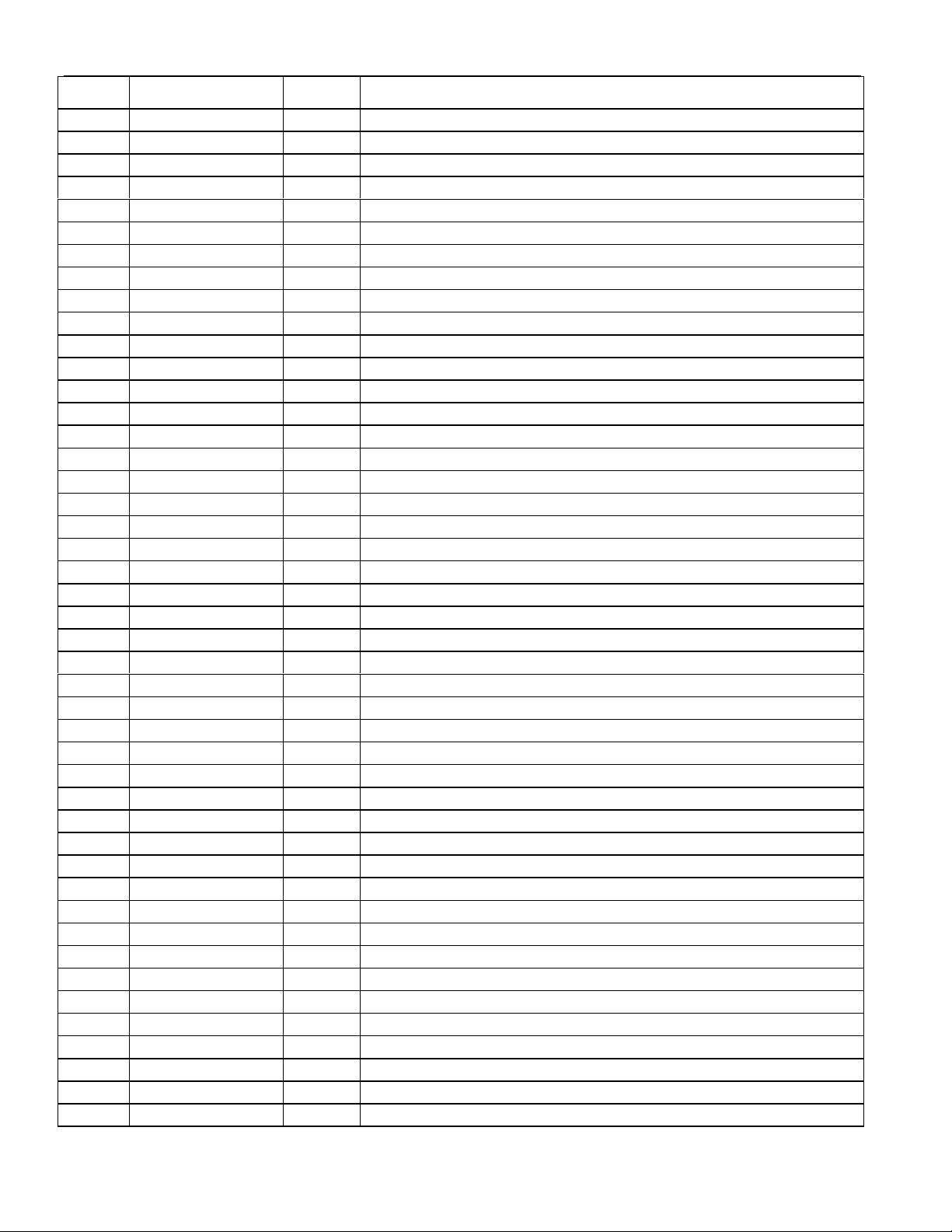
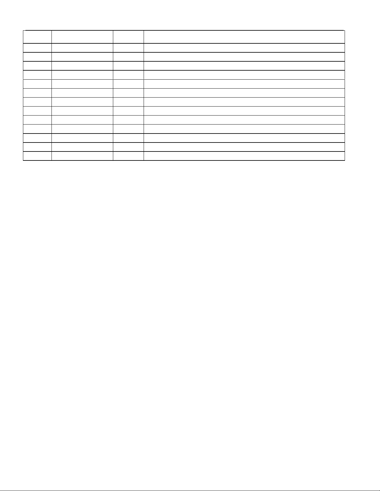
Pin Description Sorted by Pin Function, FMS = 0 Table 2-2
PIN SYMBOL TYPE DESCRIPTION
108 8MCLK O 8 MHz Clock
23 A0 I Address Bus Bit 0; LSB
24 A1 I Address Bus Bit 1
25 A2 I Address Bus Bit 2
26 A3 I Address Bus Bit 3
27 A4 I Address Bus Bit 4
28 A5 I Address Bus Bit 5
29 A6/ALE (AS) I Address Bus Bit 6; MSB or Address Latch Enable (Address
Strobe)
46 A7 I Address Bus Bit 7
61 BTS I Bus Type Select for Parallel Control Port
112 CLKSI I 8MCLK Clock Reference Input
60 CS* I Chip Select
117 D0 or AD0 I/O Data Bus Bit or Address/Data Bit 0; LSB
118 D1 or AD1 I/O Data Bus Bit or Address/Data Bit 1
119 D2 or AD2 I/O Data Bus Bit or Address/Data Bit 2
120 D3 or AD3 I/O Data Bus Bit or Address/Data Bit 3
121 D4 or AD4 I/O Data Bus Bit or Address/Data Bit 4
122 D5 or AD5 I/O Data Bus Bit or Address/Data Bit 5
123 D6 or AD6 I/O Data Bus Bit or Address/Data Bit 6
124 D7 or AD7 I/O Data Bus Bit or Address/Data Bit 7; MSB
47 FMS I Framer Mode Select
58 FS0 I Framer Select 0 for Parallel Control Port
59 FS1 I Framer Select 1 for Parallel Control Port
30 INT* O Receive Alarm Interrupt for all Four Framers
52 JTCLK I JTAG Test Clock
10 of 105
PIN SYMBOL TYPE DESCRIPTION
84 JTDI I JTAG Test Data Input
86 JTDO O JTAG Test Data Output
50 JTMS I JTAG Test Mode Select
18 JTRST* I JTAG Reset
64 MUX I Non-Multiplexed or Multiplexed Bus Select
10 RCHBLK0 O Receive Channel Block from Framer 0
44 RCHBLK1 O Receive Channel Block from Framer 1
80 RCHBLK2 O Receive Channel Block from Framer 2
104 RCHBLK3 O Receive Channel Block from Framer 3
6 RCLK0 I Receive Clock for Framer 0
40 RCLK1 I Receive Clock for Framer 1
74 RCLK2 I Receive Clock for Framer 2
100 RCLK3 I Receive Clock for Framer 3
62 RD*/(DS*) I Read Input (Data Strobe)
17 RFSYNC0 O Receive Frame Sync from Framer 0
51 RFSYNC1 O Receive Frame Sync from Framer 1
85 RFSYNC2 O Receive Frame Sync from Framer 2
109 RFSYNC3 O Receive Frame Sync from Framer 3
5 RLCLK0 O Receive Link Clock from Framer 0
39 RLCLK1 O Receive Link Clock from Framer 1
73 RLCLK2 O Receive Link Clock from Framer 2
99 RLCLK3 O Receive Link Clock from Framer 3
4 RLINK0 O Receive Link Data from Framer 0
38 RLINK1 O Receive Link Data from Framer 1
72 RLINK2 O Receive Link Data from Framer 2
98 RLINK3 O Receive Link Data from Framer 3
7 RNEG0 I Receive Bipolar Data for Framer 0
41 RNEG1 I Receive Bipolar Data for Framer 1
75 RNEG2 I Receive Bipolar Data for Framer 2
101 RNEG3 I Receive Bipolar Data for Framer 3
8 RPOS0 I Receive Bipolar Data for Framer 0
42 RPOS1 I Receive Bipolar Data for Framer 1
76 RPOS2 I Receive Bipolar Data for Framer 2
102 RPOS3 I Receive Bipolar Data for Framer 3
13 RSER0 O Receive Serial Data from Framer 0
49 RSER1 O Receive Serial Data from Framer 1
83 RSER2 O Receive Serial Data from Framer 2
107 RSER3 O Receive Serial Data from Framer 3
9 RSIG0 O Receive Signaling Output from Framer 0
43 RSIG1 O Receive Signaling output from Framer 1
77 RSIG2 O Receive Signaling Output from Framer 2
103 RSIG3 O Receive Signaling Output from Framer 3
12 RSYNC0 I/O Receive Sync for Framer 0
48 RSYNC1 I/O Receive Sync for Framer 1
82 RSYNC2 I/O Receive Sync for Framer 2
DS21Q44
11 of 105

DS21Q44
PIN SYMBOL TYPE DESCRIPTION
106 RSYNC3 I/O Receive Sync for Framer 3
11 RSYSCLK0 I Receive System Clock for Elastic Store in Framer 0
45 RSYSCLK1 I Receive System Clock for Elastic Store in Framer 1
81 RSYSCLK2 I Receive System Clock for Elastic Store in Framer 2
105 RSYSCLK3 I Receive System Clock for Elastic Store in Framer 3
16 SPARE1 - RESERVED - must be left unconnected for normal operation
1 TCHBLK0 O Transmit Channel Block from Framer 0
35 TCHBLK1 O Transmit Channel Block from Framer 1
69 TCHBLK2 O Transmit Channel Block from Framer 2
95 TCHBLK3 O Transmit Channel Block from Framer 3
19 TCLK0 I Transmit Clock for Framer 0
53 TCLK1 I Transmit Clock for Framer 1
87 TCLK2 I Transmit Clock for Framer 2
113 TCLK3 I Transmit Clock for Framer 3
57 TEST I 3-state Control for all Output and I/O Pins
20 TLCLK0 O Transmit Link Clock from Framer 0
54 TLCLK1 O Transmit Link Clock from Framer 1
88 TLCLK2 O Transmit Link Clock from Framer 2
114 TLCLK3 O Transmit Link Clock from Framer 3
22 TLINK0 I Transmit Link Data for Framer 0
56 TLINK1 I Transmit Link Data for Framer 1
90 TLINK2 I Transmit Link Data for Framer 2
116 TLINK3 I Transmit Link Data for Framer 3
3 TNEG0 O Transmit Bipolar Data from Framer 0
37 TNEG1 O Transmit Bipolar Data from Framer 1
71 TNEG2 O Transmit Bipolar Data from Framer 2
97 TNEG3 O Transmit Bipolar Data from Framer 3
2 TPOS0 O Transmit Bipolar Data from Framer 0
36 TPOS1 O Transmit Bipolar Data from Framer 1
70 TPOS2 O Transmit Bipolar Data from Framer 2
96 TPOS3 O Transmit Bipolar Data from Framer 3
126 TSER0 I Transmit Serial Data for Framer 0
32 TSER1 I Transmit Serial Data for Framer 1
66 TSER2 I Transmit Serial Data for Framer 2
92 TSER3 I Transmit Serial Data for Framer 3
128 TSIG0 I Transmit Signaling Input for Framer 0
34 TSIG1 I Transmit Signaling Input for Framer 1
68 TSIG2 I Transmit Signaling Input for Framer 2
94 TSIG3 I Transmit Signaling Input for Framer 3
127 TSSYNC0 I Transmit Sync for Elastic Store in Framer 0
33 TSSYNC1 I Transmit Sync for Elastic Store in Framer 1
67 TSSYNC2 I Transmit Sync for Elastic Store in Framer 2
93 TSSYNC3 I Transmit Sync for Elastic Store in Framer 3
21 TSYNC0 I/O Transmit Sync for Framer 0
55 TSYNC1 I/O Transmit Sync for Framer 1
12 of 105
PIN SYMBOL TYPE DESCRIPTION
89 TSYNC2 I/O Transmit Sync for Framer 2
115 TSYNC3 I/O Transmit Sync for Framer 3
125 TSYSCLK0 I Transmit System Clock for Elastic Store in Framer 0
31 TSYSCLK1 I Transmit System Clock for Elastic Store in Framer 1
65 TSYSCLK2 I Transmit System Clock for Elastic Store in Framer 2
91 TSYSCLK3 I Transmit System Clock for Elastic Store in Framer 3
15 VDD - Positive Supply Voltage
79 VDD - Positive Supply Voltage
111 VDD - Positive Supply Voltage
14 VSS - Signal Ground
78 VSS - Signal Ground
110 VSS - Signal Ground
63 WR*/(R/W*) I Write Input (Read/Write)
3. DS21Q44 PIN FUNCTIO N DESCRI PTION
TRANSMIT SIDE PINS
Signal Name:
Signal Description:
Signal Type:
A 2.048 MHz primary clock. Used to clock data through the transmit side formatter.
TCLK
Transmit Clock
Input
DS21Q44
Signal Name:
Signal Description:
Signal Type:
Transmit NRZ serial data. Sampled on the falling edge of TCLK when the transmit side elastic store is
disabled. Sampled on the falling edge of TSYSCLK when the transmit side elastic store is enabled.
Signal Name:
Signal Description:
Signal Type:
A 256 KHz clock which pulses high during the LSB of each channel. Synchronous with TCLK when the
transmit side elastic store is disabled. Synchronous with TSYSCLK when the transmit side elastic store is
enabled. Useful for parallel to serial conversion of channel data. This function is available when FMS = 1
(DS21Q43 emulation).
Signal Name:
Signal Description:
Signal Type:
A user programmable output that can be forced high or low during any of the 32 E1 channels.
Synchronous with TCLK when the transmit side elastic store is disabled. Synchronous with TSYSCLK
when the transmit side elastic store is enabled. Useful for blocking clocks to a serial UART or LAPD
controller in applications where not all E1 channels are used such as Fractional E1, 384 Kbps (H0), 768
Kbps, 1920 bps (H12) or ISDN–PRI . Also useful for locating individual channels in drop–and–insert
applications, for external per–channel loopback, and for per–channel conditioning. See Section 12 for
details.
TSER
Transmit Serial Data
Input
TCHCLK
Transmit Channel Clock
Output
TCHBLK
Transmit Channel Block
Output
13 of 105

DS21Q44
Signal Name:
Signal Description:
Signal Type:
TSYSCLK
Transmit System Clock
Input
1.544 MHz or 2.048 MHz clock. Only used when the transmit side elastic store function is enabled.
Should be tied low in applications that do not use the transmit side elastic store. Can be burst at rates up
to 8.192 MHz.
Signal Name:
Signal Description:
Signal Type:
TLCLK
Transmit Link Clock
Output
4 KHz to 20 KHz demand clock for the TLINK input. See Section 14 for details.
Signal Name:
Signal Description:
Signal Type:
TLINK
Transmit Link Data
Input
If enabled, this pin will be sampled on the falling edge of TCLK for data insertion into any combination
of the Sa bit positions (Sa4 to Sa8). See Section 14 for details.
Signal Name:
Signal Description:
Signal Type:
TSYNC
Transmit Sync
Input /Output
A pulse at this pin will establish either frame or multiframe boundaries for the transmit side. This pin can
also be programmed to output either a frame or multiframe pulse. Always synchronous with TCLK.
Signal Name:
Signal Description:
Signal Type:
TSSYNC
Transmit System Sync
Input
Only used when the transmit side elastic store is enabled. A pulse at this pin will establish either frame or
multiframe boundaries for the transmit side. Should be tied low in applications that do not use the
transmit side elastic store. Always synchronous with TSYSCLK.
Signal Name:
Signal Description:
Signal Type:
TSIG
Transmit Signaling Input
Input
When enabled, this input will sample signaling bits for insertion into outgoing PCM E1 data stream.
Sampled on the falling edge of TCLK when the transmit side elastic store is disabled. Sampled on the
falling edge of TSYSCLK when the transmit side elastic store is enabled. This function is available when
FMS = 0.
Signal Name:
Signal Description:
Signal Type:
TPOS
Transmit Positive Data Output
Output
Updated on the rising edge of TCLK with the bipolar data out of the transmit side formatter. Can be
programmed to source NRZ data via the Output Data Format (TCR1.7) control bit.
Signal Name:
Signal Description:
Signal Type:
TNEG
Transmit Negative Data Output
Output
Updated on the rising edge of TCLK with the bipolar data out of the transmit side formatter.
14 of 105

RECEIVE SIDE PINS
Signal Name:
Signal Description:
Signal Type:
Updated with full recovered E1 data stream on the rising edge of RCLK.
RLINK
Receive Link Data
Output
DS21Q44
Signal Name:
Signal Description:
Signal Type:
RLCLK
Receive Link Clock
Output
A 4 KHz to 20 KHz clock for the RLINK output. Used for sampling Sa bits.
Signal Name:
Signal Description:
Signal Type:
RCLK
Receive Clock Input
Input
2.048 MHz clock that is used to clock data through the receive side framer.
Signal Name:
Signal Description:
Signal Type:
RCHCLK
Receive Channel Clock
Output
A 256 KHz clock which pulses high during the LSB of each channel. Synchronous with RCLK when the
receive side elastic store is disabled. Synchronous with RSYSCLK when the receive side elastic store is
enabled. Useful for parallel to serial conversion of channel data. This function is available when FMS = 1
(DS21Q43 emulation).
Signal Name:
Signal Description:
Signal Type:
RCHBLK
Receive Channel Block
Output
A user programmable output that can be forced high or low during any of the 32 E1 channels.
Synchronous with RCLK when the receive side elastic store is disabled. Synchronous with RSYSCLK
when the receive side elastic store is enabled. Useful for blocking clocks to a serial UART or LAPD
controller in applications where not all E1 channels are used such as Fractional E1, 384K bps service,
768K bps, or ISDN–PRI. Also useful for locating individual channels in drop–and–insert applications, for
external per–channel loopback, and for per–channel conditioning. See Section 12 for details.
Signal Name:
Signal Description:
Signal Type:
RSER
Receive Serial Data
Output
Received NRZ serial data. Updated on rising edges of RCLK when the receive side elastic store is
disabled. Updated on the rising edges of RSYSCLK when the receive side elastic store is enabled.
Signal Name:
Signal Description:
Signal Type:
RSYNC
Receive Sync
Input /Output
An extracted pulse, one RCLK wide, is output at this pin which identifies either frame or CAS/CRC
multiframe boundaries. If the receive side elastic store is enabled, then this pin can be enabled to be an
input at which a frame or multiframe boundary pulse synchronous with RSYSCLK is applied.
15 of 105

Signal Name:
Signal Description:
Signal Type:
RFSYNC
Receive Frame Sync
Output
An extracted 8 KHz pulse, one RCLK wide, is output at this pin which identifies frame boundaries.
DS21Q44
Signal Name:
Signal Description:
Signal Type:
RMSYNC
Receive Multiframe Sync
Output
An extracted pulse, one RSYSCLK wide, is output at this pin which identifies multiframe boundaries. If
the receive side elastic store is disabled, then this output will output multiframe boundaries associated
with RCLK. This function is available when FMS = 1 (DS21Q43 emulation).
Signal Name:
Signal Description:
Signal Type:
RSYSCLK
Receive System Clock
Input
1.544 MHz or 2.048 MHz clock. Only used when the elastic store function is enabled. Should be tied low
in applications that do not use the elastic store. Can be burst at rates up to 8.192 MHz.
Signal Name:
Signal Description:
Signal Type:
RSIG
Receive Signaling Output
Output
Outputs signaling bits in a PCM format. Updated on rising edges of RCLK when the receive side elastic
store is disabled. Updated on the rising edges of RSYSCLK when the receive side elastic store is enabled.
This function is available when FMS = 0.
Signal Name:
Signal Description:
Signal Type:
RLOS/LOTC
Receive Loss of Sync / Loss of Transmit Clock
Output
A dual function output that is controlled by the TCR2.0 control bit. This pin can be programmed to either
toggle high when the synchronizer is searching for the frame and multiframe or to toggle high if the
TCLK pin has not been toggled for 5 usec. This function is available when FMS = 1 (DS21Q43
emulation).
Signal Name:
Signal Description:
Signal Type:
CLKSI
8 MHz Clock Reference
Input
A 2.048 MHz reference clock used in the generation of 8MCLK. This function is available when
FMS = 0.
Signal Name:
Signal Description:
Signal Type:
8MCLK
8 MHz Clock
Output
A 8.192 MHz output clock that is referenced to the clock that is input at the CLKSI pin. This function is
available when FMS = 0.
16 of 105

DS21Q44
Signal Name:
Signal Description:
Signal Type:
RPOS
Receive Positive Data Input
Input
Sampled on the falling edge of RCLK for data to be clocked through the receive side framer. RPOS and
RNEG can be tied together for an NRZ interface. Connecting RPOS to RNEG disables the bipolar
violation monitoring circuitry.
Signal Name:
Signal Description:
Signal Type:
RNEG
Receive Negative Data Input
Input
Sampled on the falling edge of RCLK for data to be clocked through the receive side framer. RPOS and
RNEG can be tied together for an NRZ interface. Connecting RPOS to RNEG disables the bipolar
violation monitoring circuitry.
PARALLEL CONTROL PORT PINS
Signal Name:
Signal Description:
Signal Type:
Flags host controller during conditions and change of conditions defined in the Status Registers 1 and 2
and the FDL Status Register. Active low, open drain output.
Signal Name:
Signal Description:
Signal Type:
Set low to select DS21Q44 feature set. Set high to select DS21Q43 emulation.
Signal Name:
Signal Description:
Signal Type:
Set low to select non–multiplexed bus operation. Set high to select multiplexed bus operation.
INT*
Interrupt
Output
FMS
Framer Mode Select
Input
MUX
Bus Operation
Input
Signal Name:
Signal Description:
Signal Type:
D0 TO D7 / AD0 TO AD7
Data Bus or Address/Data Bus
Input /Output
In non–multiplexed bus operation (MUX = 0), serves as the data bus. In multiplexed bus operation (MUX
= 1), serves as a 8–bit multiplexed address / data bus.
Signal Name:
Signal Description:
Signal Type:
A0 TO A5, A7
Address Bus
Input
In non–multiplexed bus operation (MUX = 0), serves as the address bus. In multiplexed bus operation
(MUX = 1), these pins are not used and should be tied low.
Signal Name:
Signal Description:
Signal Type:
ALE (AS) / A6
Address Latch Enable (Address Strobe) or A6
Input
In non–multiplexed bus operation (MUX = 0), serves as address bit 6. In multiplexed bus operation
(MUX = 1), serves to demultiplex the bus on a positive–going edge.
17 of 105

DS21Q44
Signal Name:
Signal Description:
Signal Type:
BTS
Bus Type Select
Input
Strap high to select Motorola bus timing; strap low to select Intel bus timing. This pin controls the
function of the RD*(DS*), ALE(AS), and WR*(R/W*) pins. If BTS = 1, then these pins assume the
function listed in parenthesis ().
Signal Name:
Signal Description:
Signal Type:
RD* (DS*)
Read Input (Data Strobe)
Input
RD* and DS* are active low signals. Note: DS is active high when MUX=1. Refer to bus timing
diagrams in section 19 .
Signal Name:
Signal Description:
Signal Type:
FS0 AND FS1
Framer Selects
Input
Selects which of the four framers to be accessed.
Signal Name:
Signal Description:
Signal Type:
CS*
Chip Select
Input
Must be low to read or write to the device. CS* is an active low signal.
Signal Name:
Signal Description:
Signal Type:
WR* (R/W*)
Write Input (Read/Write)
Input
WR* is an active low signal.
TEST ACCESS PORT PINS
Signal Name:
Signal Description:
Signal Type:
Set high to 3–state all output and I/O pins (including the parallel control port). Set low for normal
operation. Useful in board level testing.
Signal Name:
Signal Description:
Signal Type:
This signal is used to asynchronously reset the test access port controller. At power up, JTRST* must be
set low and then high. This action will set the device into the boundary scan bypass mode allowing
normal device operation. If boundary scan is not used, this pin should be held low. This function is
available when FMS = 0.
Signal Name:
Signal Description:
Signal Type:
This pin is sampled on the rising edge of JTCLK and is used to place the test port into the various defined
IEEE 1149.1 states. If not used, this pin should be pulled high. This function is available when FMS = 0.
TEST
3–State Control
Input
JTRST*
IEEE 1149.1 Test Reset
Input
JTMS
IEEE 1149.1 Test Mode Select
Input
18 of 105

DS21Q44
Signal Name:
Signal Description:
Signal Type:
JTCLK
IEEE 1149.1 Test Clock Signal
Input
This signal is used to shift data into JTDI on the rising edge and out of JTDO on the falling edge. If not
used, this pin should be tied to VSS. This function is available when FMS = 0.
Signal Name:
Signal Description:
Signal Type:
JTDI
IEEE 1149.1 Test Data Input
Input
Test instructions and data are clocked into this pin on the rising edge of JTCLK. If not used, this pin
should be pulled high. This function is available when FMS = 0.
Signal Name:
Signal Description:
Signal Type:
JTDO
IEEE 1149.1 Test Data Output
Output
Test instructions and data are clocked out of this pin on the falling edge of JTCLK. If not used, this pin
should be left unconnected. This function is available when FMS = 0.
SUPPLY PINS
Signal Name:
Signal Description:
Signal Type:
2.97 to 3.63 volts.
Signal Name:
Signal Description:
Signal Type:
0.0 volts.
VDD
Positive Supply
Supply
VSS
Signal Ground
Supply
19 of 105
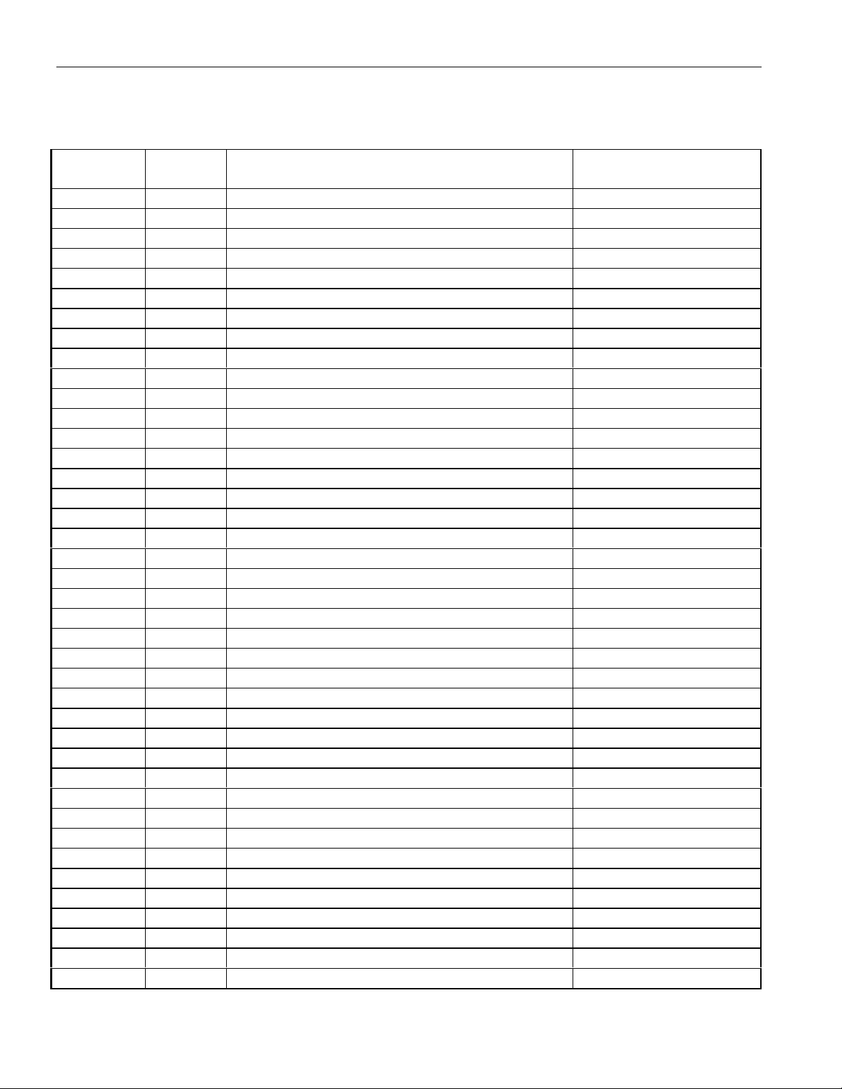
4. DS21Q44 REGISTER MAP
Register Map Sorted by Address Table 4-1
REGISTER
ADDRESS R/W REGISTER NAME
00 R BPV or Code Violation Count 1 VCR1
01 R BPV or Code Violation Count 2 VCR2
02 R CRC4 Error Count 1 / FAS Error Count 1 CRCCR1
03 R CRC4 Error Count 2 CRCCR2
04 R E-Bit Count 1 / FAS Error Count 2 EBCR1
05 R E-Bit Count 2 EBCR2
06 R/W Status 1 SR1
07 R/W Status 2 SR2
08 R/W Receive Information RIR
09 R/W Test 2 TEST2 (set to 00h)
0A – Not used (set to 00H)
0B – Not used (set to 00H)
0C – Not used (set to 00H)
0D – Not used (set to 00H)
0E – Not used (set to 00H)
0F R Device ID IDR
10 R/W Receive Control 1 RCR1
11 R/W Receive Control 2 RCR2
12 R/W Transmit Control 1 TCR1
13 R/W Transmit Control 2 TCR2
14 R/W Common Control 1 CCR1
15 R/W Test 1 TEST1 (set to 00h)
16 R/W Interrupt Mask 1 IMR1
17 R/W Interrupt Mask 2 IMR2
18 – Not used (set to 00H)
19 – Not used (set to 00H)
1A R/W Common Control 2 CCR2
1B R/W Common Control 3 CCR3
1C R/W Transmit Sa Bit Control TSaCR
1D R/W Common Control 6 CCR6
1E R Synchronizer Status SSR
1F R Receive Non-Align Frame RNAF
20 R/W Transmit Align Frame TAF
21 R/W Transmit Non-Align Frame TNAF
22 R/W Transmit Channel Blocking 1 TCBR1
23 R/W Transmit Channel Blocking 2 TCBR2
24 R/W Transmit Channel Blocking 3 TCBR3
25 R/W Transmit Channel Blocking 4 TCBR4
26 R/W Transmit Idle 1 TIR1
27 R/W Transmit Idle 2 TIR2
ABBREVIATION
DS21Q44
20 of 105
REGISTER
ADDRESS R/W REGISTER NAME
ABBREVIATION
28 R/W Transmit Idle 3 TIR3
29 R/W Transmit Idle 4 TIR4
2A R/W Transmit Idle Definition TIDR
2B R/W Receive Channel Blocking 1 RCBR1
2C R/W Receive Channel Blocking 2 RCBR2
2D R/W Receive Channel Blocking 3 RCBR3
2E R/W Receive Channel Blocking 4 RCBR4
2F R Receive Align Frame RAF
30 R Receive Signaling 1 RS1
31 R Receive Signaling 2 RS2
32 R Receive Signaling 3 RS3
33 R Receive Signaling 4 RS4
34 R Receive Signaling 5 RS5
35 R Receive Signaling 6 RS6
36 R Receive Signaling 7 RS7
37 R Receive Signaling 8 RS8
38 R Receive Signaling 9 RS9
39 R Receive Signaling 10 RS10
3A R Receive Signaling 11 RS11
3B R Receive Signaling 12 RS12
3C R Receive Signaling 13 RS13
3D R Receive Signaling 14 RS14
3E R Receive Signaling 15 RS15
3F R Receive Signaling 16 RS16
40 R/W Transmit Signaling 1 TS1
41 R/W Transmit Signaling 2 TS2
42 R/W Transmit Signaling 3 TS3
43 R/W Transmit Signaling 4 TS4
44 R/W Transmit Signaling 5 TS5
45 R/W Transmit Signaling 6 TS6
46 R/W Transmit Signaling 7 TS7
47 R/W Transmit Signaling 8 TS8
48 R/W Transmit Signaling 9 TS9
49 R/W Transmit Signaling 10 TS10
4A R/W Transmit Signaling 11 TS11
4B R/W Transmit Signaling 12 TS12
4C R/W Transmit Signaling 13 TS13
4D R/W Transmit Signaling 14 TS14
4E R/W Transmit Signaling 15 TS15
4F R/W Transmit Signaling 16 TS16
50 R/W Transmit Si Bits Align Frame TSiAF
51 R/W Transmit Si Bits Non-Align Frame TSiNAF
52 R/W Transmit Remote Alarm Bits TRA
53 R/W Transmit Sa4 Bits TSa4
DS21Q44
21 of 105

ADDRESS R/W REGISTER NAME
ABBREVIATION
54 R/W Transmit Sa5 Bits TSa5
55 R/W Transmit Sa6 Bits TSa6
56 R/W Transmit Sa7 Bits TSa7
57 R/W Transmit Sa8 Bits TSa8
58 R Receive Si bits Align Frame RSiAF
59 R Receive Si bits Non-Align Frame RSiNAF
5A R Receive Remote Alarm Bits RRA
5B R Receive Sa4 Bits RSa4
5C R Receive Sa5 Bits RSa5
5D R Receive Sa6 Bits RSa6
5E R Receive Sa7 Bits RSa7
5F R Receive Sa8 Bits RSa8
60 R/W Transmit Channel 1 TC1
61 R/W Transmit Channel 2 TC2
62 R/W Transmit Channel 3 TC3
63 R/W Transmit Channel 4 TC4
64 R/W Transmit Channel 5 TC5
65 R/W Transmit Channel 6 TC6
66 R/W Transmit Channel 7 TC7
67 R/W Transmit Channel 8 TC8
68 R/W Transmit Channel 9 TC9
69 R/W Transmit Channel 10 TC10
6A R/W Transmit Channel 11 TC11
6B R/W Transmit Channel 12 TC12
6C R/W Transmit Channel 13 TC13
6D R/W Transmit Channel 14 TC14
6E R/W Transmit Channel 15 TC15
6F R/W Transmit Channel 16 TC16
70 R/W Transmit Channel 17 TC17
71 R/W Transmit Channel 18 TC18
72 R/W Transmit Channel 19 TC19
73 R/W Transmit Channel 20 TC20
74 R/W Transmit Channel 21 TC21
75 R/W Transmit Channel 22 TC22
76 R/W Transmit Channel 23 TC23
77 R/W Transmit Channel 24 TC24
78 R/W Transmit Channel 25 TC25
79 R/W Transmit Channel 26 TC26
7A R/W Transmit Channel 27 TC27
7B R/W Transmit Channel 28 TC28
7C R/W Transmit Channel 29 TC29
7D R/W Transmit Channel 30 TC30
7E R/W Transmit Channel 31 TC31
7F R/W Transmit Channel 32 TC32
DS21Q44
REGISTER
22 of 105

REGISTER
ADDRESS R/W REGISTER NAME
ABBREVIATION
80 R/W Receive Channel 1 RC1
81 R/W Receive Channel 2 RC2
82 R/W Receive Channel 3 RC3
83 R/W Receive Channel 4 RC4
84 R/W Receive Channel 5 RC5
85 R/W Receive Channel 6 RC6
86 R/W Receive Channel 7 RC7
87 R/W Receive Channel 8 RC8
88 R/W Receive Channel 9 RC9
89 R/W Receive Channel 10 RC10
8A R/W Receive Channel 11 RC11
8B R/W Receive Channel 12 RC12
8C R/W Receive Channel 13 RC13
8D R/W Receive Channel 14 RC14
8E R/W Receive Channel 15 RC15
8F R/W Receive Channel 16 RC16
90 R/W Receive Channel 17 RC17
91 R/W Receive Channel 18 RC18
92 R/W Receive Channel 19 RC19
93 R/W Receive Channel 20 RC20
94 R/W Receive Channel 21 RC21
95 R/W Receive Channel 22 RC22
96 R/W Receive Channel 23 RC23
97 R/W Receive Channel 24 RC24
98 R/W Receive Channel 25 RC25
99 R/W Receive Channel 26 RC26
9A R/W Receive Channel 27 RC27
9B R/W Receive Channel 28 RC28
9C R/W Receive Channel 29 RC29
9D R/W Receive Channel 30 RC30
9E R/W Receive Channel 31 RC31
9F R/W Receive Channel 32 RC32
A0 R/W Transmit Channel Control 1 TCC1
A1 R/W Transmit Channel Control 2 TCC2
A2 R/W Transmit Channel Control 3 TCC3
A3 R/W Transmit Channel Control 4 TCC4
A4 R/W Receive Channel Control 1 RCC1
A5 R/W Receive Channel Control 2 RCC2
A6 R/W Receive Channel Control 3 RCC3
A7 R/W Receive Channel Control 4 RCC4
A8 R/W Common Control 4 CCR4
A9 R Transmit DS0 Monitor TDS0M
AA R/W Common Control 5 CCR5
AB R Receive DS0 Monitor RDS0M
DS21Q44
23 of 105
REGISTER
ADDRESS R/W REGISTER NAME
AC R/W Test 3 TEST3 (set to 00H)
AD – Not used (set to 00H)
AE – Not used (set to 00H)
AF – Not used (set to 00H)
B0 R/W HDLC Control Register HCR
B1 R/W HDLC Status Register HSR
B2 R/W HDLC Interrupt Mask Register HIMR
B3 R/W Receive HDLC Information Register RHIR
B4 R/W Receive HDLC FIFO Register RHFR
B5 R/W Interleave Bus Operation Register IBO
B6 R/W Transmit HDLC Information Register THIR
B7 R/W Transmit HDLC FIFO Register THFR
B8 R/W Receive HDLC DS0 Control Register 1 RDC1
B9 R/W Receive HDLC DS0 Control Register 2 RDC2
BA R/W Transmit HDLC DS0 Control Register 1 TDC1
BB R/W Transmit HDLC DS0 Control Register 2 TDC2
BC – Not used (set to 00H)
BD – Not used (set to 00H)
BE – Not used (set to 00H)
BF – Not used (set to 00H)
ABBREVIATION
DS21Q44
Notes:
1. Test Registers 1, 2, and 3 are used only by the factory; these registers must be cleared (set to all
zeros) on power– up initialization to insure proper operation.
2. Register banks CxH, DxH, ExH, and FxH are not accessible.
5. PARALLEL PORT
The DS21Q44 is controlled via either a non–multiplexed (MUX = 0) or a multiplexed (MUX = 1) bus b y
an external microcontroller or microprocessor. The DS21Q44 can operate with either Intel or Motorola
bus timing configurations. If the BTS pin is tied low, Intel timing will be selected; if tied high, Motorola
timing will be selected. All Motorola bus signals are listed in parenthesis (). See the timing diagrams in
the A.C. Electrical Characteristics in Section 19 for more details.
6. CONTROL, ID AND TEST REGISTERS
The operation of each framer within the DS21Q44 is configured via a set of ten control registers.
Typically, the control registers are only accessed when the system is first powered up. Once a channel in
the DS21Q44 has been initialized, the control registers will only need to be accessed when there is a
change in the system configuration. There are two Receive Control Register (RCR1 and RCR2), two
Transmit Control Registers (TCR1 and TCR2), and six Common Control Registers (CCR1 to CCR6).
Each of the ten registers are described in this section.
There is a device Identification Register (IDR) at address 0Fh. The MSB of this read–only register is
fixed to a one indicating that the DS21Q44 is present. The T1 pin–for–pin compatible version of the
DS21Q44 is the DS21Q42 and it also has an ID register at address 0Fh and the user can read the MSB to
determine which chip is present since in the DS21Q42 the MSB will be set to a zero and in the DS21Q44
it will be set to a one. The lower four bits of the IDR are used to display the die revision of the chip.
24 of 105
DS21Q44
Power–Up Sequence
The DS21Q44 does not automatically clear its register space on power–up. After the supplies are stable,
each of the four framer’s register space should be con fi gured for operation by writing to all of the internal
registers. This includes setting the Test and all unused registers to 00Hex.
This can be accomplished using a two-pass approach on each framer within the DS21Q44.
1. Clear framer’s register space by writing 00H to the addresses 00H through 0BFH.
2. Program required registers to achieve desired operating mode.
Note:
When emulating the DS21Q43 feature set (FMS = 1), the full address space (00H through 0BFH) must be
initialized. DS21Q43 emulation require address pin A7 to be used.
Finally, after the TSYSCLK and RSYSCLK inputs are stable, the ESR bit should be toggled from a zero
to a one (this step can be skipped if the elastic stores are disabled).
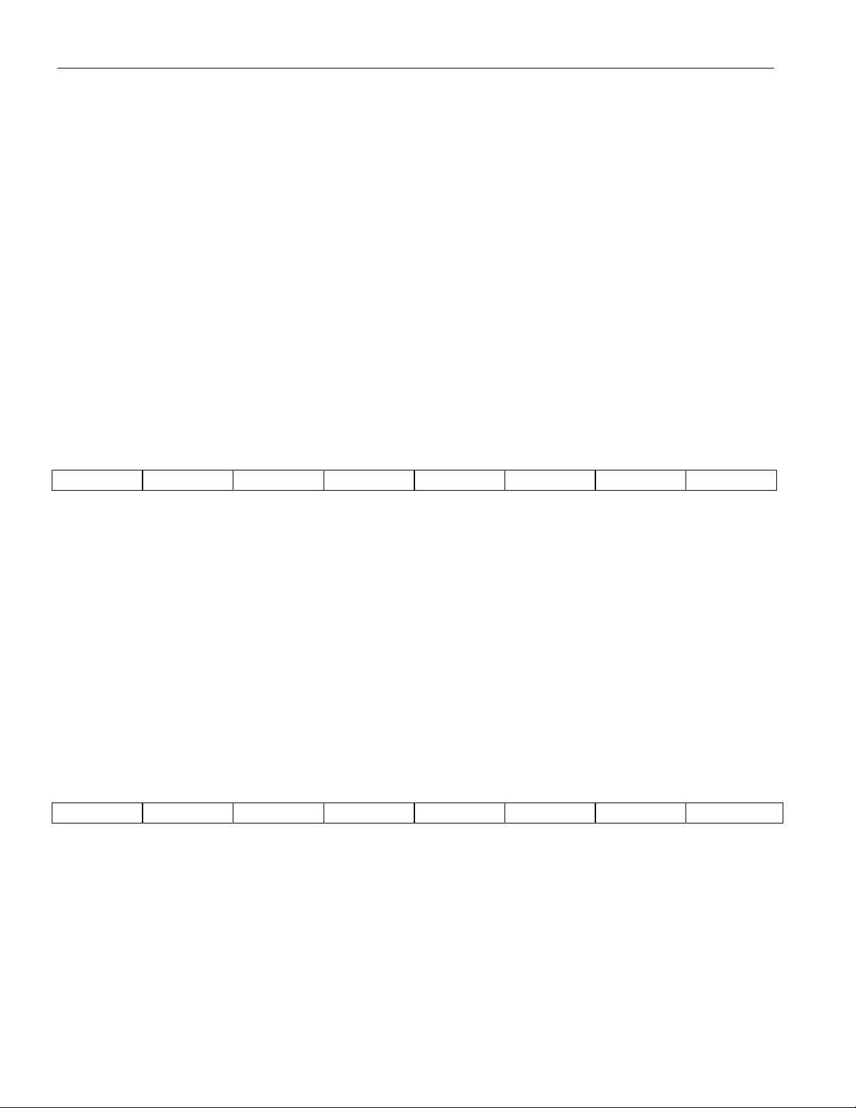
IDR: DEVICE IDENTIFICATION REGISTER (Address=0F Hex)
(MSB) (LSB)
T1E1 0 0 0 ID3 ID2 ID1 ID0
SYMBOL POSITION NAME AND DESCRIPTION
T1E1 IDR.7
ID3 IDR.3 Chip Revision Bit 3. MSB of a decimal code that represents the
ID2 IDR.1
ID1 IDR.2
ID0 IDR.0 Chip Revision Bit 0. LSB of a decimal code that represents the
T1 or E1 Chip Determination Bit.
0=T1 chip
1=E1 chip
chip revision.
Chip Revision Bit 2.
Chip Revision Bit 1.
chip revision.
RCR1: RECEIVE CONTROL REGISTER 1 (Address=10 Hex)
(MSB) (LSB)
RSMF RSM RSIO – – FRC SYNCE RESYNC
SYMBOL POSITION NAME AND DESCRIPTION
RSMF RCR1.7 RSYNC Multiframe Function. Only used if the RSYNC pin is
programmed in the multiframe mode (RCR1.6=1).
0 = RSYNC outputs CAS multiframe boundaries
1 = RSYNC outputs CRC4 multiframe boundaries
RSM RCR1.6
RSYNC Mode Select.
0 = frame mode (see the timing in Section 18)
1 = multiframe mode (see the timing in Section 18)
25 of 105

SYMBOL POSITION NAME AND DESCRIPTION
RSIO RCR1.5 RSYNC I/O Select. (note: this bit must be set to zero when
RCR2.1=0).
0 = RSYNC is an output (depends on RCR1.6)
1 = RSYNC is an input (only valid if elastic store enabled)
– RCR1.4 Not Assigned. Should be set to zero when written.
– RCR1.3 Not Assigned. Should be set to zero when written.
FRC RCR1.2
Frame Resync Criteria.
0 = resync if FAS received in error 3 consecutive times
1 = resync if FAS or bit 2 of non–FAS is received in error 3
consecutive times
SYNCE RCR1.1
Sync Enable.
0 = auto resync enabled
1 = auto resync disabled
RESYNC RCR1.0 Resync. When toggled from low to high, a resync is initiated.
Must be cleared and set again for a subsequent resync.
SYNC/RESYNC CRITERIA Table 6–1
DS21Q44
FRAME OR
SYNC CRITERIA RESYNC CRITERIA ITU SPEC.
MULTIFRAME
LEVEL
FAS FAS present in frame N and
N + 2, and FAS not present in
frame N + 1
CRC4 Two valid MF alignment
words found within 8 ms
CAS Valid MF alignment word
found and previous timeslot
16 contains code other than all
zeros
Three consecutive incorrect
FAS received
Alternate (RCR1.2=1) the
above criteria is met or three
consecutive incorrect bit 2 of
non–FAS received
915 or more CRC4 code
words out of 1000 received in
error
Two consecutive MF
alignment words received in
error
G.706
4.1.1
4.1.2
G.706
4.2 and 4.3.2
G.732 5.2
26 of 105
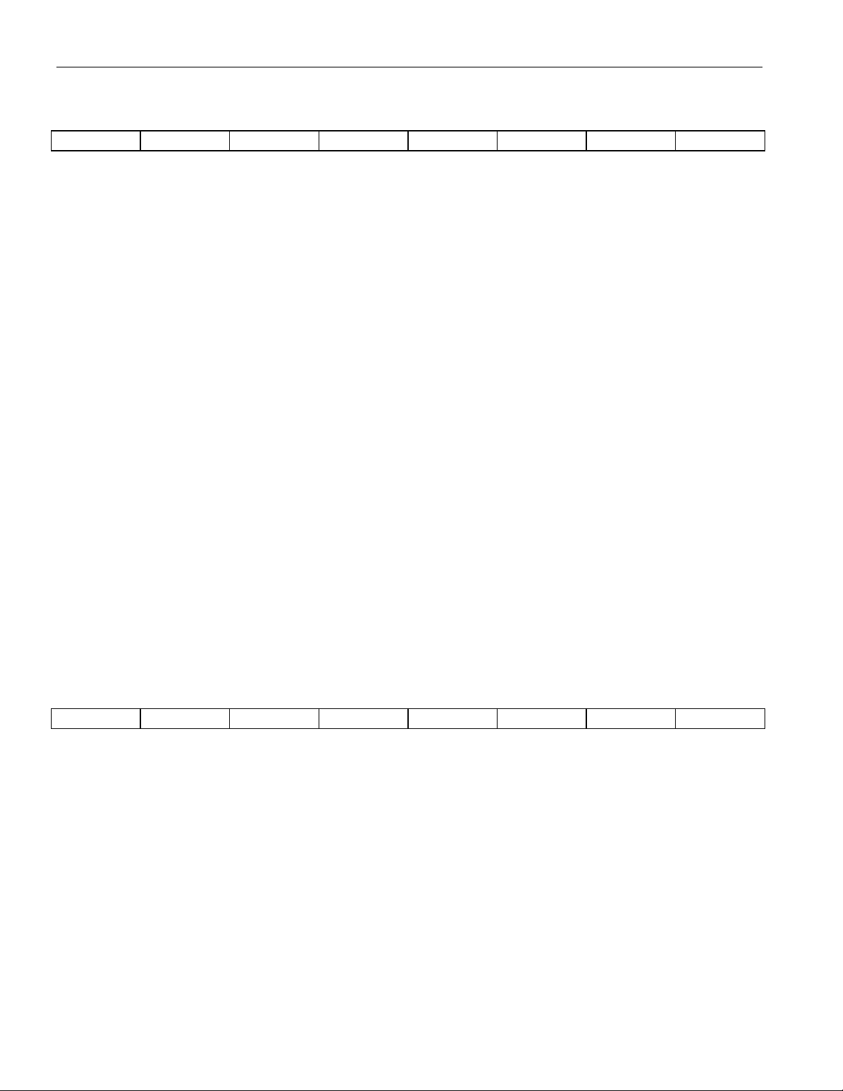
RCR2: RECEIVE CONTROL REGISTER 2 (Address=11 Hex)
(MSB) (LSB)
Sa8S Sa7S Sa6S Sa5S Sa4S RBCS RESE –
SYMBOL POSITION NAME AND DESCRIPTION
Sa8S RCR2.7 Sa8 Bit Select. Set to one to have RLCLK pulse at the Sa8 bit
position; set to zero to force RLCLK low during Sa8 bit
position. See Section 18 for timing details.
Sa7S RCR2.6 Sa7 Bit Select. Set to one to have RLCLK pulse at the Sa7 bit
position; set to zero to force RLCLK low during Sa7 bit
position. See Section 18 for timing details.
Sa6S RCR2.5 Sa6 Bit Select. Set to one to have RLCLK pulse at the Sa6 bit
position; set to zero to force RLCLK low during Sa6 bit
position. See Section 18 for timing details.
Sa5S RCR2.4 Sa5 Bit Select. Set to one to have RLCLK pulse at the Sa5 bit
position; set to zero to force RLCLK low during Sa5 bit
position. See Section 18 for timing details.
Sa4S RCR2.3 Sa4 Bit Select. Set to one to have RLCLK pulse at the Sa4 bit
position; set to zero to force RLCLK low during Sa4 bit
position. See Section 18 for timing details.
RBCS RCR2.2
RESE RCR2.1
– RCR2.0 Not Assigned. Should be set to zero when written.
Receive Side Backplane Clock Select.
0 = if RSYSCLK is 1.544 MHz
1 = if RSYSCLK is 2.048 MHz
Receive Side Elastic Store Enable.
0 = elastic store is bypassed
1 = elastic store is enabled
DS21Q44
TCR1: TRANSMIT CONTROL REGISTER 1 (Address=12 Hex)
(MSB) (LSB)
ODF TFPT T16S TUA1 TSiS TSA1 TSM TSIO
SYMBOL POSITION NAME AND DESCRIPTION
ODF TCR1.7
TFPT TCR1.6
T16S TCR1.5
27 of 105
Output Data Format.
0 = bipolar data at TPOS and TNEG
1 = NRZ data at TPOS; TNEG=0
Transmit Timeslot 0 Pass Through.
0 = FAS bits/Sa bits/Remote Alarm sourced internally from the
TAF and TNAF registers
1 = FAS bits/Sa bits/Remote Alarm sourced from TSER
Transmit Timeslot 16 Data Select.
0 = sample timeslot 16 at TSER pin
1 = source timeslot 16 from TS0 to TS15 registers
SYMBOL POSITION NAME AND DESCRIPTION
DS21Q44
TUA1 TCR1.4
TSiS TCR1.3
TSA1 TCR1.2
TSM CR1.1
TSIO TCR1.0
Transmit Unframed All Ones.
0 = transmit data normally
1 = transmit an unframed all one’s code at TPOS and TNEG
Transmit International Bit Select.
0 = sample Si bits at TSER pin
1 = source Si bits from TAF and TNAF registers (in this mode,
TCR1.6 must be set to 0)
Transmit Signaling All Ones.
0 = normal operation
1 = force timeslot 16 in every frame to all ones
TSYNC Mode Select.
0 = frame mode (see the timing in Section 18)
1 = CAS and CRC4 multiframe mode (see the timing in Section
18)
TSYNC I/O Select.
0 = TSYNC is an input
1 = TSYNC is an output
Notes:
See Figure 18–15 for more details about how the Transmit Control Registers affect the operation of the
DS21Q44.
TCR2: TRANSMIT CONTROL REGISTER 2 (Address=13 Hex)
(MSB) (LSB)
Sa8S Sa7S Sa6S Sa5S Sa4S ODM AEBE PF
SYMBOL POSITION NAME AND DESCRIPTION
Sa8S TCR2.7 Sa8 Bit Select. Set to one to source the Sa8 bit from the TLINK
pin; set to zero to not source the Sa8 bit. See Section 18 for
timing details.
Sa7S TCR2.6 Sa7 Bit Select. Set to one to source the Sa7 bit from the TLINK
pin; set to zero to not source the Sa7 bit. See Section 18 for
timing details.
Sa6S TCR2.5 Sa6 Bit Select. Set to one to source the Sa6 bit from the TLINK
pin; set to zero to not source the Sa6 bit. See Section 18 for
timing details.
Sa5S TCR2.4 Sa5 Bit Select. Set to one to source the Sa5 bit from the TLINK
pin; set to zero to not source the Sa5 bit. See Section 18 for
timing details.
Sa4S TCR2.3 Sa4 Bit Select. Set to one to source the Sa4 bit from the TLINK
pin; set to zero to not source the Sa4 bit. See Section 18 for
timing details.
28 of 105
SYMBOL POSITION NAME AND DESCRIPTION
DS21Q44
ODM TCR2.2
Output Data Mode.
0 = pulses at TPOSO and TNEGO are one full TCLKO period
wide
1 = pulses at TPOSO and TNEGO are 1/2 TCLKO period wide
AEBE TCR2.1
Automatic E–Bit Enable.
0 = E–bits not automatically set in the transmit direction
1 = E–bits automatically set in the transmit direction
PF TCR2.0
Function of RLOS/LOTC Pin.
0 = Receive Loss of Sync (RLOS)
1 = Loss of Transmit Clock (LOTC)
CCR1: COMMON CONTROL REGISTER 1 (Address=14 Hex)
(MSB) (LSB)
FLB THDB3 TG802 TCRC4 RSM RHDB3 RG802 RCRC4
SYMBOL POSITION NAME AND DESCRIPTION
FLB CCR1.7
THDB3 CCR1.6
TG802 CCR1.5 Transmit G.802 Enable. See Section 18 for details.
TCRC4 CCR1.4
RSM CCR1.3
RHDB3 CCR1.2
RG802 CCR1.1 Receive G.802 Enable. See Section 18 for details.
RCRC4 CCR1.0
Framer Loopback.
0=loopback disabled
1=loopback enabled
Transmit HDB3 Enable.
0=HDB3 disabled
1=HDB3 enabled
0=do not force TCHBLK high during bit 1 of timeslot 26
1=force TCHBLK high during bit 1 of timeslot 26
Transmit CRC4 Enable.
0=CRC4 disabled
1=CRC4 enabled
Receive Signaling Mode Select.
0=CAS signaling mode
1=CCS signaling mode
Receive HDB3 Enable.
0=HDB3 disabled
1=HDB3 enabled
0=do not force RCHBLK high during bit 1 of timeslot 26
1=force RCHBLK high during bit 1 of timeslot 26
Receive CRC4 Enable.
0=CRC4 disabled
1=CRC4 enabled
29 of 105
DS21Q44
FRAMER LOOPBACK
When CCR1.7 is set to a one, the framer will enter a Framer LoopBack (FLB) mode. See Figure 1–1 for
more details. This loopback is useful in testing and debugging applications. In FLB, the framer will loop
data from the transmit side back to the receive side. When FLB is enabled, the following will occur:
1. Data will be transmitted as normal at TPOS and TNEG.
2. Data input via RPOS and RNEG will be ignored.
3. The RCLK output will be replaced with the TCLK input.
CCR2: COMMON CONTROL REGISTER 2 (Address=1A Hex)
(MSB) (LSB)
ECUS VCRFS AAIS ARA RSERC LOTCMC RFF RFE
SYMBOL POSITION NAME AND DESCRIPTION
ECUS CCR2.7 Error Counter Update Select. See Section 8 for details.
0=update error counters once a second
1=update error counters every 62.5 ms (500 frames)
VCRFS CCR2.6 VCR Function Select. See Section 8 for details.
0=count BiPolar Violations (BPVs)
1=count Code Violations (CVs)
AAIS CCR2.5
ARA CCR2.4
RSERC CCR2.3
LOTCMC CCR2.2 Loss of Transmit Clock Mux Control. Determines whether
RFF CCR2.1 Receive Force Freeze. Freezes receive side signaling at RSIG
RFE CCR2.0 Receive Freeze Enable. See Section 10 for details.
Automatic AIS Generation.
0=disabled
1=enabled
Automatic Remote Alarm Generation.
0=disabled
1=enabled
RSER Control.
0=allow RSER to output data as received under all conditions
1=force RSER to one under loss of frame alignment conditions
the transmit side formatter should switch to the ever present
RCLK if the TCLK should fail to transition (see Figure 1–1).
0=do not switch to RCLK if TCLK stops
1=switch to RCLK if TCLK stops
(and RSER if CCR3.3=1); will override Receive Freeze Enable
(RFE). See Section 10 or details.
0=do not force a freeze event
1=force a freeze event
0=no freezing of receive signaling data will occur
1=allow freezing of receive signaling data at RSIG (and RSER
if CCR3.3=1).
30 of 105
 Loading...