Dallas Semiconductor DS21Q43ATN, DS21Q43AT Datasheet
FEATURES
DS21Q43A
Quad E1 Framer
www.dalsemi.com
§ Four E1 (CEPT or PCM-30) /ISDN-PRI
framing transceivers
§ All four framers are fully independent;
transmit and receive sections of each framer
are fully independent
§ Frames to FAS, CAS, CCS, and CRC4
formats
§ 8-bit parallel control port that can be
connected to either multiplexed or nonmultiplexed buses
§ Each of the four framers contains dual two-
frame elastic stores that can connect to
asynchronous or synchronous backplanes up
to 8.192 MHz
§ Easy access to Si and Sa bits
§ Extracts and inserts CAS signaling
§ Large counters for bipolar and code
violations, CRC4 code word errors, FAS
word errors, and E-bits
§ Programmable output clocks for Fractional
E1, per channel loopback, H0 and H12
applications
§ Detects and generates AIS, remote alarm, and
remote multiframe alarms
§ Pin-compatible with DS21Q41B Quad T1
Framer
§ 5V supply; low power CMOS
§ Available in 128-pin TQFP
§ Industrial (-40°C to +85°C) grade version
available (DS21Q43ATN)
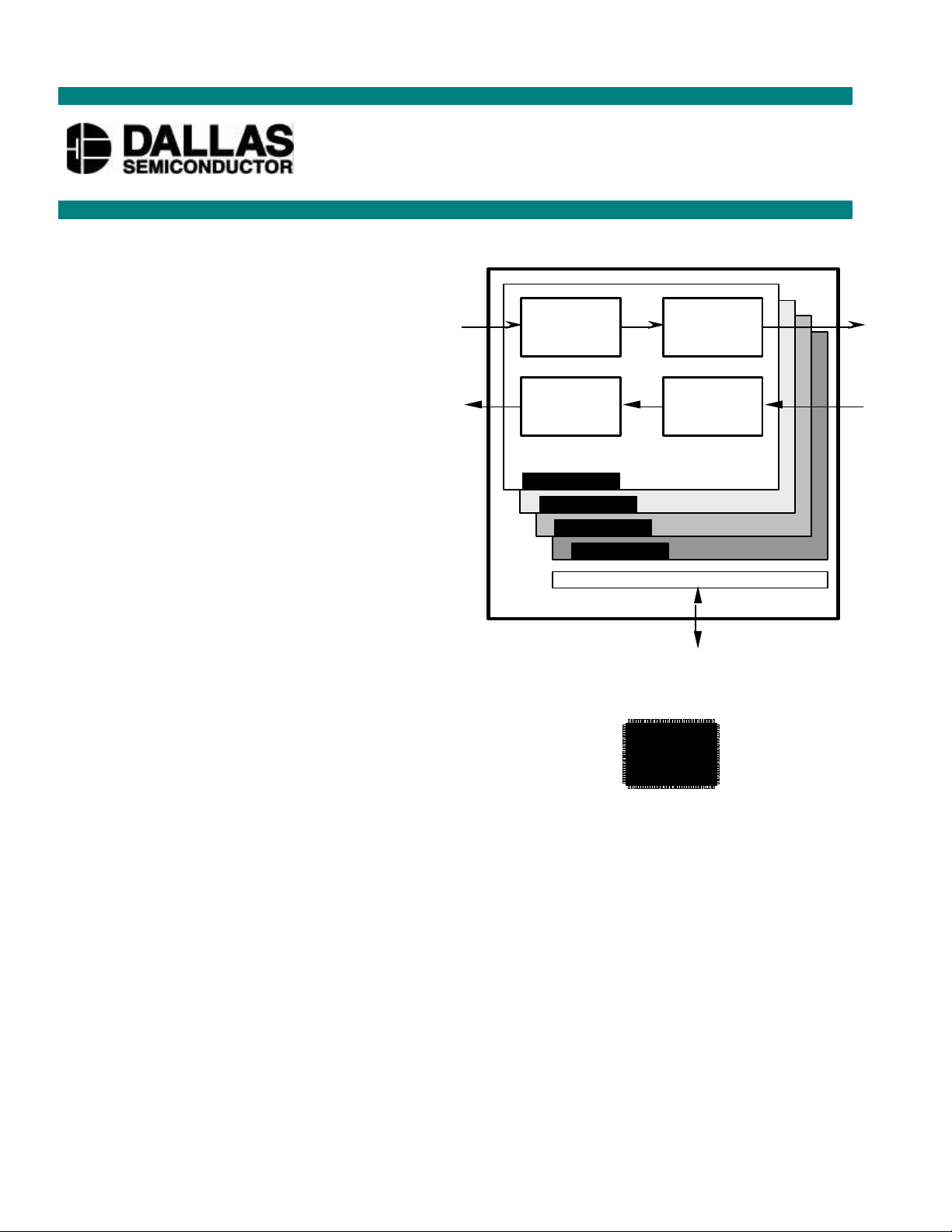
FUNCTIONAL DIAGRAM
RECEIVE
FRAMER
TRANSMIT
FORMATTER
FRAMER #0
FRAMER #1
FRAMER #2
FRAMER #3
ELASTIC
STORE
ELASTIC
STORE
CONTROL PORT
ACTUAL SIZE
QUAD
E1
FRAMER
DESCRIPTION
The DS21Q43A combines four of the popular DS2143 E1 Controllers onto a single monolithic die. The
“A” designation denotes that some new features are available in the Quad version which were not
available in the single E1 device. The added features in the DS21Q43A are listed in Section 1. The
DS21Q43A offers a substantial space savings to applications that require more than one E1 framer on a
card. The Quad version is only slightly bigger than the single E1 device. All four framers in the
DS21Q43A are totally independent; they do not share a common framing synchronizer. Also, the transmit
and receive sides of each framer are totally independent. The dual two-frame elastic stores contained in
each of the four framers can be independently enabled and disabled as required. The DS21Q43A meets
all of the latest specifications, including CCITT/ITU G.704, G.706, G.962, and I.431 as well as ETS 300
011 and ETS 300 233.
1 of 60 092299

DS21Q43A
1.0 INTRODUCTION
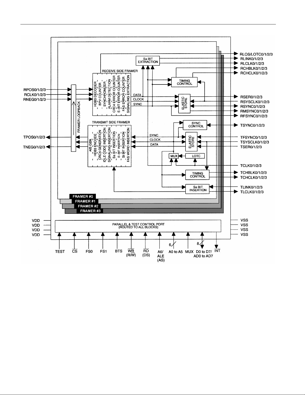
The DS21Q43A Quad E1 Framer is made up of five main parts: framer #0, framer #1, framer #2, framer
#3, and the control port which is shared by all four framers. See the Block Diagram in Figure 1-1. Each
of the four framers within the DS21Q43A maintains the same register structure that appeared in the
DS2143. The two framer-select inputs (FS0 and FS1) are used to determine which framer within the
DS21Q43A is being accessed. In this manner, software written for the DS2143 can also be used in the
DS21Q43A with only slight modifications. Several new features have been added to the framers in the
DS21Q43A over the DS2143.
ADDED FEATURE SECTION
Non-multiplexed parallel control port operation 2 and 13
Transmit side elastic store 10
Expanded access to Sa and Si bits 6
Control signals RFSYNC, RMSYNC, and TFSYNC 1
FAS word error counting 5
Code violation counting 5
Automatic AIS generation upon loss of frame sync 3
Automatic remote alarm generation 3
Per-channel signaling insertion 9 and 11
Per-channel loopback from RSER to TSER 8 and 11
Option to update error counters every 62.5 ms 5
CRC4 resync criteria met status bit 4
Elastic store reset 10
Hardware 3-state control 1
2 of 60
DS21Q43A BLOCK DIAGRAM Figure 1-1
DS21Q43A
READER’S NOTE
This data sheet assumes a particular nomenclature of the E1 operating environment. There are 32 8-bit
timeslots in an E1 system which are numbered 0 to 31. Timeslot 0 is transmitted first and received first.
These 32 timeslots are also referred to as channels with a numbering scheme of 1 to 32. Timeslot 0 is
identical to channel 1, timeslot 1 is identical to channel 2, and so on. Each timeslot (or channel) is made
up of 8 bits which are numbered 1 to 8. Bit number 1 is the MSB and is transmitted first. Bit number 8 is
the LSB and is transmitted last. Throughout this data sheet, the following abbreviations will be used:
FAS Frame Alignment CRC4 Cyclical Redundancy Check
CAS Channel Associated CCS Common Channel Signaling
Signaling
MF Multiframe Sa Additional bits
Si International bits E-bit CRC4 Error bits
3 of 60
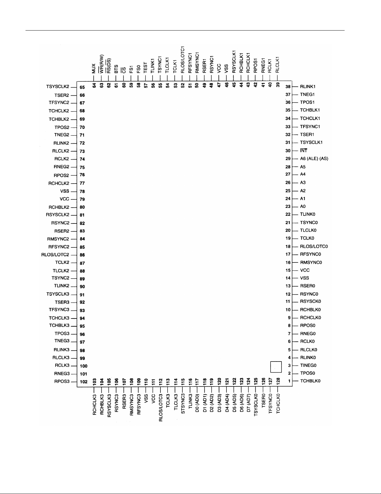
PIN-OUT CONFIGURATION Figure 1-2
DS21Q43A
4 of 60
TRANSMIT PIN LIST Table 1-1
PIN SYMBOL TYPE DESCRIPTION
19 TCLK0 I Transmit Clock for Framer 0
53 TCLK1 I Transmit Clock for Framer 1
87 TCLK2 I Transmit Clock for Framer 2
113 TCLK3 I Transmit Clock for Framer 3
126 TSER0 I Transmit Serial Data for Framer 0
32 TSER1 I Transmit Serial Data for Framer 1
66 TSER2 I Transmit Serial Data for Framer 2
92 TSER3 I Transmit Serial Data for Framer 3
128 TCHCLK0 O Transmit Channel Clock from Framer 0
34 TCHCLK1 O Transmit Channel Clock from Framer 1
68 TCHCLK2 O Transmit Channel Clock from Framer 2
94 TCHCLK3 O Transmit Channel Clock from Framer 3
1 TCHBLK0 O Transmit Channel Block from Framer 0
35 TCHBLK1 O Transmit Channel Block from Framer 1
DS21Q43A
69 TCHBLK2 O Transmit Channel Block from Framer 2
95 TCHBLK3 O Transmit Channel Block from Framer 3
20 TLCLK0 O Transmit Link Clock from Framer 0
54 TLCLK1 O Transmit Link Clock from Framer 1
88 TLCLK2 O Transmit Link Clock from Framer 2
114 TLCLK3 O Transmit Link Clock from Framer 3
22 TLINK0 I Transmit Link Data for Framer 0
56 TLINK1 I Transmit Link Data for Framer 1
90 TLINK2 I Transmit Link Data for Framer 2
116 TLINK3 I Transmit Link Data for Framer 3
2 TPOS0 O Transmit Bipolar Data from Framer 0
36 TPOS1 O Transmit Bipolar Data from Framer 1
70 TPOS2 O Transmit Bipolar Data from Framer 2
96 TPOS3 O Transmit Bipolar Data from Framer 3
3 TNEG0 O Transmit Bipolar Data from Framer 0
37 TNEG1 O Transmit Bipolar Data from Framer 1
71 TNEG2 O Transmit Bipolar Data from Framer 2
97 TNEG3 O Transmit Bipolar Data from Framer 3
21 TSYNC0 I/O Transmit Sync for Framer 0
55 TSYNC1 I/O Transmit Sync for Framer 1
89 TSYNC2 I/O Transmit Sync for Framer 2
115 TSYNC3 I/O Transmit Sync for Framer 3
5 of 60
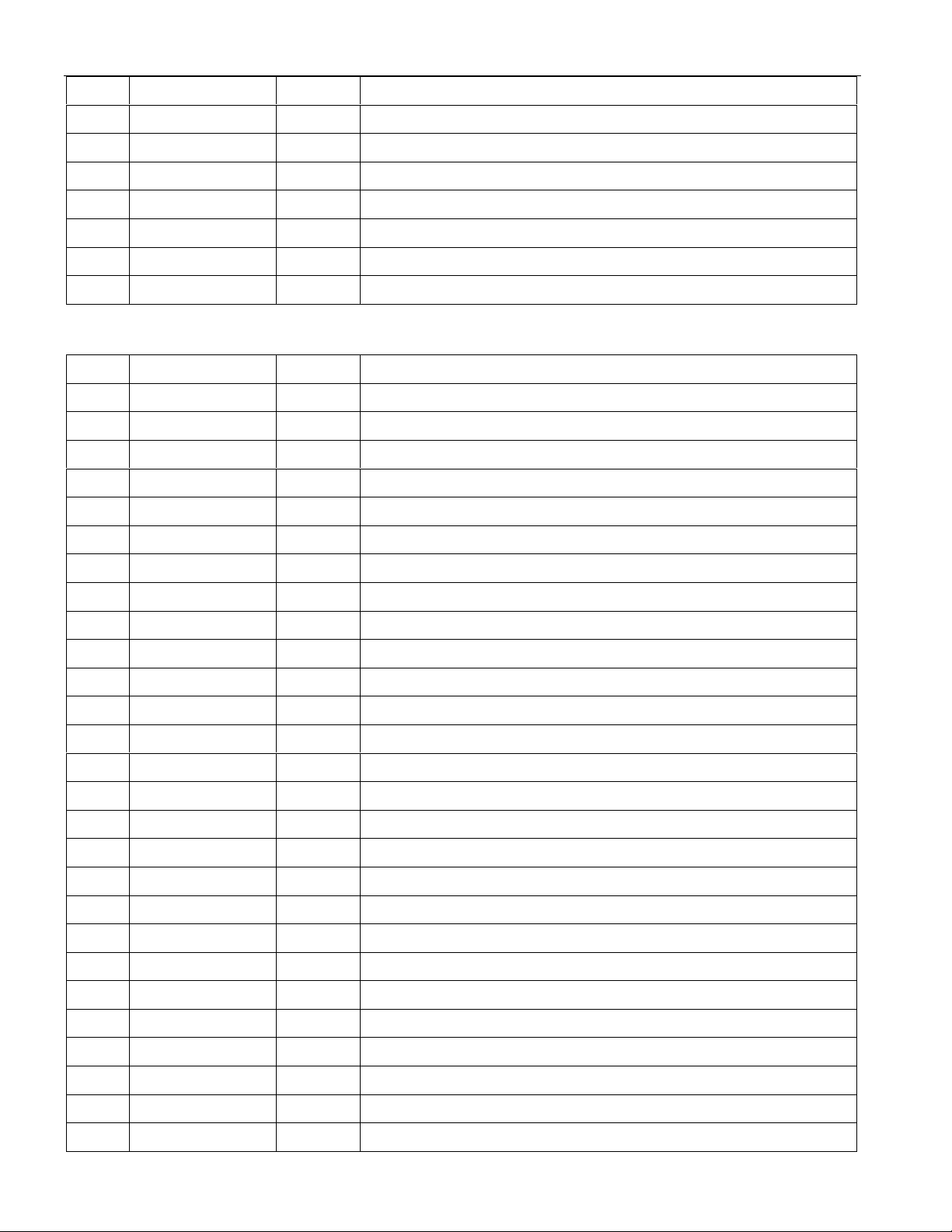
127 TFSYNC0 I Transmit Sync for Elastic Store in Framer 0
33 TFSYNC1 I Transmit Sync for Elastic Store in Framer 1
67 TFSYNC2 I Transmit Sync for Elastic Store in Framer 2
93 TFSYNC3 I Transmit Sync for Elastic Store in Framer 3
125 TSYSCLK0 I Transmit System Clock for Elastic Store in Framer 0
31 TSYSCLK1 I Transmit System Clock for Elastic Store in Framer 1
65 TSYSCLK2 I Transmit System Clock for Elastic Store in Framer 2
91 TSYSCLK3 I Transmit System Clock for Elastic Store in Framer 3
RECEIVE PIN LIST Table 1-2
PIN SYMBOL TYPE DESCRIPTION
6 RCLK0 I Receive Clock for Framer 0
40 RCLK1 I Receive Clock for Framer 1
74 RCLK2 I Receive Clock for Framer 2
100 RCLK3 I Receive Clock for Framer 3
13 RSER0 O Receive Serial Data from Framer 0
DS21Q43A
49 RSER1 O Receive Serial Data from Framer 1
83 RSER2 O Receive Serial Data from Framer 2
107 RSER3 O Receive Serial Data from Framer 3
9 RCHCLK0 O Receive Channel Clock from Framer 0
43 RCHCLK1 O Receive Channel Clock from Framer 1
77 RCHCLK2 O Receive Channel Clock from Framer 2
103 RCHCLK3 O Receive Channel Clock from Framer 3
10 RCHBLK0 O Receive Channel Block from Framer 0
44 RCHBLK1 O Receive Channel Block from Framer 1
80 RCHBLK2 O Receive Channel Block from Framer 2
104 RCHBLK3 O Receive Channel Block from Framer 3
5 RLCLK0 O Receive Link Clock from Framer 0
39 RLCLK1 O Receive Link Clock from Framer 1
73 RLCLK2 O Receive Link Clock from Framer 2
99 RLCLK3 O Receive Link Clock from Framer 3
4 RLINK0 O Receive Link Data from Framer 0
38 RLINK1 O Receive Link Data from Framer 1
72 RLINK2 O Receive Link Data from Framer 2
98 RLINK3 O Receive Link Data from Framer 3
8 RPOS0 I Receive Bipolar Data for Framer 0
42 RPOS1 I Receive Bipolar Data for Framer 1
76 RPOS2 I Receive Bipolar Data for Framer 2
6 of 60

102 RPOS3 I Receive Bipolar Data for Framer 3
7 RNEG0 I Receive Bipolar Data for Framer 0
41 RNEG1 I Receive Bipolar Data for Framer 1
75 RNEG2 I Receive Bipolar Data for Framer 2
101 RNEG3 I Receive Bipolar Data for Framer 3
12 RSYNC0 I/O Receive Sync for Framer 0
48 RSYNC1 I/O Receive Sync for Framer 1
82 RSYNC2 I/O Receive Sync for Framer 2
106 RSYNC3 I/O Receive Sync for Framer 3
17 RFSYNC0 O Receive Frame Sync from Framer 0
51 RFSYNC1 O Receive Frame Sync from Framer 1
85 RFSYNC2 O Receive Frame Sync from Framer 2
109 RFSYNC3 O Receive Frame Sync from Framer 3
16 RMSYNC0 O Receive Multiframe Sync from Framer 0
50 RMSYNC1 O Receive Multiframe Sync from Framer 1
DS21Q43A
84 RMSYNC2 O Receive Multiframe Sync from Framer 2
108 RMSYNC3 O Receive Multiframe Sync from Framer 3
11 RSYSCLK0 I Receive System Clock for Elastic Store in Framer 0
45 RSYSCLK1 I Receive System Clock for Elastic Store in Framer 1
81 RSYSCLK2 I Receive System Clock for Elastic Store in Framer 2
105 RSYSCLK3 I Receive System Clock for Elastic Store in Framer 3
18 RLOS/LOTC0 O Receive Loss of Sync/Loss of Transmit Clock from Framer 0
52 RLOS/LOTC1 O Receive Loss of Sync/Loss of Transmit Clock from Framer 1
86 RLOS/LOTC2 O Receive Loss of Sync/Loss of Transmit Clock from Framer 2
112 RLOS/LOTC3 O Receive Loss of Sync/Loss of Transmit Clock from Framer 3
7 of 60
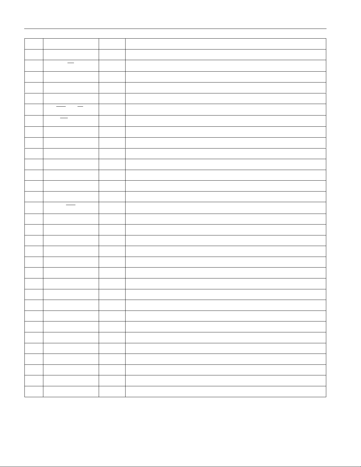
CONTROL PORT/TEST/SUPPLY PIN LIST Table 1-3
RD
PIN SYMBOL TYPE DESCRIPTION
57 TEST I 3-State Control for all Output and I/O Pins.
DS21Q43A
60
CS
I Chip Select.
58 FS0 I Framer Select 0 for Parallel Control Port.
59 FS1 I Framer Select 1 for Parallel Control Port.
61 BTS I Bus Type Select for Parallel Control Port.
63
62
WR (R/W )
(DS)
I Write Input (Read/Write).
I Read Input (Data Strobe).
23 A0 I Address Bus Bit 0; LSB.
24 A1 I Address Bus Bit 1.
25 A2 I Address Bus Bit 2.
26 A3 I Address Bus Bit 3.
27 A4 I Address Bus Bit 4.
28 A5 I Address Bus Bit 5.
29 A6 or ALE (AS) I Address Bus Bit 6; MSB or Address Latch Enable (Address Strobe).
30
INT
O Receive Alarm Interrupt for all Four Framers.
64 MUX I Non-Multiplexed or Multiplexed Bus Select.
117 D0 or AD0 I/O Data Bus Bit 0 or Address/Data Bus Bit 0; LSB.
118 D1 or AD1 I/O Data Bus Bit 1 or Address/Data Bus Bit 1.
119 D2 or AD2 I/O Data Bus Bit 2 or Address/Data Bus Bit 2.
120 D3 or AD3 I/O Data Bus Bit 3 or Address/Data Bus Bit 3.
121 D4 or AD4 I/O Data Bus Bit 4 or Address/Data Bus Bit 4.
122 D5 or AD5 I/O Data Bus Bit 5 or Address/Data Bus Bit 5.
123 D6 or AD6 I/O Data Bus Bit 6 or Address/Data Bus Bit 6.
124 D7 or AD7 I/O Data Bus Bit 7 or Address/Data Bus Bit 7; MSB.
15 V
47 V
79 V
111 V
14 V
46 V
78 V
110 V
DD
DD
DD
DD
SS
SS
SS
SS
- Positive Supply Voltage.
- Positive Supply Voltage.
- Positive Supply Voltage.
- Positive Supply Voltage.
- Signal Ground.
- Signal Ground.
- Signal Ground.
- Signal Ground.
8 of 60

DS21Q43A
DS21Q43A PIN DESCRIPTION Table 1-4
Transmit Clock [TCLK]. 2.048 MHz primary clock. Used to clock data through the transmit side
formatter. Necessary for proper operation of the parallel control port.
Transmit Serial Data [TSER]. Transmit NRZ serial data. Sampled on the falling edge of TCLK when
the transmit side elastic store is disabled. Sampled on the falling edge of TSYSCLK when the transmit
side elastic store is enabled.
Transmit Channel Clock [TCHCLK]. 256 kHz clock which pulses high during the LSB of each
channel. Synchronous with TCLK when the transmit side elastic store is disabled. Synchronous with
TSYSCLK when the transmit side elastic store is enabled. Useful for parallel to serial conversion of
channel data. See Section 11 for timing details.
Transmit Bipolar Data [TPOS and TNEG]. Updated on rising edge of TCLK. Can be programmed to
output NRZ data on TPOS via the TCR1.7 control bit.
Transmit Channel Block [TCHBLK]. A user programmable output that can be forced high or low
during any of the 32 E1 channels. Synchronous with TCLK when the transmit side elastic store is
disabled. Synchronous with TSYSCLK when the transmit side elastic store is enabled. Useful for
blocking clocks to a serial UART or LAPD controller in applications where not all E1 channels are used
such as Fractional E1, 384 kpbs service (H0), 1920 kpbs (H12), or ISDN-PRI. Also useful for locating
individual channels in drop-and-insert applications and for per-channel loopback. See Section 11 for
timing details.
Transmit System Clock [TSYSCLK]. 1.544 MHz or 2.048 MHz clock. Only used when the transmit
side elastic store function is enabled. Should be tied low in applications that do not use the transmit side
elastic store.
Transmit Link Clock [TLCLK]. 4 kHz to 20 kHz demand clock for the TLINK input. Controlled by
TCR2. See Section 11 for timing details.
Transmit Link Data [TLINK]. If enabled via TCR2, this pin will be sampled on the falling edge of
TCLK to insert data into the Sa bit positions. See Section 11 for timing details.
Transmit Sync [TSYNC]. A pulse at this pin will establish either frame or multiframe boundaries for the
DS21Q43A. Via TCR1.1, the DS21Q43A can be programmed to output either a frame or multiframe
pulse at this pin. See Section 11 for timing details.
Transmit Frame Sync [TFSYNC]. 8 kHz pulse. Only used when the transmit side elastic store is
enabled. A pulse at this pin will establish frame boundaries for the DS21Q43A. Should be tied low in
applications that do not use the transmit side elastic store. See Section 11 for timing details.
Receive Link Data [RLINK]. Updated with full received E1 data stream on the rising edge of RCLK.
See Section 11 for timing details.
Receive Link Clock [RLCLK]. 4 kHz to 20 kHz demand clock for the RLINK output. Controlled by
RCR2. See Section 11 for timing details. Necessary for proper operation of the parallel control port.
Receive Clock [RCLK]. 2.048 MHz primary clock. Used to clock data through the receive side of the
framer. Necessary for proper operation of the parallel control port.
9 of 60

DS21Q43A
Receive Channel Clock [RCHCLK]. 256 kHz clock which pulses high during the LSB of each channel.
Synchronous with RCLK when the receive side elastic store is disabled. Synchronous with RSYSCLK
when the receive side elastic store is enabled. Useful for parallel to serial conversion of channel data. See
Section 11 for timing details.
Receive Channel Block [RCHBLK]. A user programmable output that can be forced high or low during
any of the 32 E1 channels. Synchronous with RCLK when the transmit side elastic store is disabled.
Synchronous with RSYSCLK when the transmit side elastic store is enabled. Useful for blocking clocks
to a serial UART or LAPD controller in applications where not all E1 channels are used such as
Fractional E1, 384 kpbs service (H0), 1920 kpbs (H12), or ISDN-PRI. Also useful for locating individual
channels in drop-and-insert applications and for per-channel loopback. See Section 11 for timing details.
Receive Serial Data [RSER]. Received NRZ serial data. Updated on rising edges of RCLK when the
receive side elastic store is disabled. Updated on the rising edges of RSYSCLK when the receive side
elastic store is enabled.
Receive Sync [RSYNC]. An extracted pulse, one RCLK wide, is output at this pin which identifies either
frame (RCR1.6=0) or multiframe boundaries (RCR1.6=1). If the receive side elastic store is enabled via
RCR2.1, then this pin can be enabled to be an input at which a frame boundary pulse is applied. See
Section 11 for timing details.
Receive Frame Sync [RFSYNC]. An extracted 8 kHz pulse, one RCLK wide, is output at this pin which
identifies frame boundaries. See Section 11 for timing details.
Receive Multiframe Sync [RMSYNC]. Only used when the receive side elastic store is enabled. An
extracted pulse, one RSYSCLK wide, is output at this pin which identifies either CAS or CRC4
multiframe boundaries. If the receive side elastic store is disabled, then this output should be ignored. See
Section 11 for timing details.
Receive Bipolar Data Inputs [RPOS and RNEG]. Sampled on falling edge of RCLK. Tie together to
receive NRZ data and disable bipolar violation monitoring circuitry.
Receive System Clock [RSYSCLK]. 1.544 MHz or 2.048 MHz clock. Only used when the elastic store
function is enabled. Should be tied low in applications that do not use the elastic store. Allowing this pin
to float can cause the device to 3-state its outputs.
Receive Loss of Sync/Loss of Transmit Clock [RLOS/LOTC]. A dual function output. If CCR1.6=0,
then this pin will toggle high when the synchronizer is searching for the E1 frame or multiframe. If
TCR2.0=1, then this pin will toggle high the TCLK pin has not been toggled for 5 µs.
Receive Alarm Interrupt [ INT ]. Flags host controller during conditions defined in the Status Registers
of the four framers. User can poll the Interrupt Status Register (ISR) to determine which status register in
which framer is active (if any). Active low, open drain output.
3-State Control [TEST]. Set high to 3-state all output and I/O pins (including the parallel control port).
Set low for normal operation. Useful in board-level testing.
Bus Operation [MUX]. Set low to select non-multiplexed bus operation. Set high to select multiplexed
bus operation.
10 of 60
DS21Q43A
Data Bus [D0 to D7] or Address/Data Bus [AD0 to AD7]. In non-multiplexed bus operation (MUX=0),
serves as the data bus. In multiplexed bus operation (MUX=1), serves as an 8-bit multiplexed
address/data bus.
Address Bus [A0 to A5]. In non-multiplexed bus operation (MUX=0), serves as the address bus. In
multiplexed bus operation (MUX=1), these pins are not used and should be tied low.
Bus Type Select [BTS]. Strap high to select Motorola bus timing; strap low to select Intel bus timing.
This pin controls the function of the RD(DS), ALE(AS), and WR (R/ W ) pins. If BTS=1, then these pins
assume the function listed in parentheses ().
Read Input [RD] (Data Strobe [DS]).
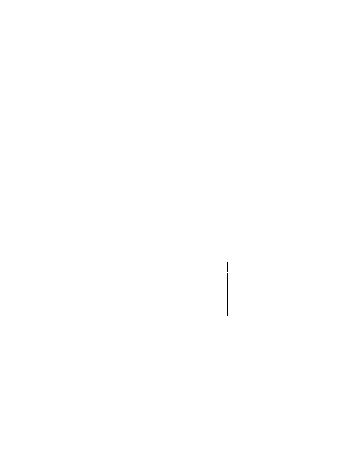
Framer Selects [FS0 and FS1]. Selects which of the four framers to be accessed.
Chip Selects [CS ]. Must be low to read or write to any of the four framers.
A6 or Address Latch Enable [ALE] (Address Strobe [AS]). In non-multiplexed bus operation
(MUX=0), serves as the upper address bit. In multiplexed bus operation (MUX=1), serves to demultiplex
the bus on a positive-going edge.
Write Input [WR ] (Read/Write [R/W ]).
Positive Supply [VDD]. 5.0 volts ± 0.5 volts.
Signal Ground [VSS]. 0.0 volts.
DS21Q43A FRAMER DECODE Table 1-5
FS1 FS0 FRAMER ACCESSED
0 0 #0
0 1 #1
1 0 #2
1 1 #3
11 of 60

DS21Q43A REGISTER MAP Table 1-6
ADDRESS R/W REGISTER NAME
00 R BPV or Code Violation Count 1.
01 R BPV or Code Violation Count 2
02 R CRC4 Count 1/FAS Error Count 1.
03 R CRC4 Error Count 2.
04 R E-Bit Count 1/FAS Error Count 2.
05 R E-Bit Count 2.
06 R Status 1.
07 R Status 2.
08 R/W Receive Information.
09 to 0F - Not Used.
(2) R Interrupt Status Register.
10 R/W Receive Control 1.
11 R/W Receive Control 2.
12 R/W Transmit Control 1.
DS21Q43A
13 R/W Transmit Control 2.
14 R/W Common Control 1.
15 R/W Test 1.
16 R/W Interrupt Mask.
17 R/W Interrupt Mask.
18 R/W Test 3.
19 R/W Test 2.
1A R/W Common Control 2.
1B R/W Common Control 3.
1C R/W Transmit Sa Control Register.
1D - Not Used.
1E R Synchronizer Status.
1F R Receive Non-Align Frame.
20 R/W Transmit Align Frame.
21 R/W Transmit Non-Align Frame.
22 R/W Transmit Channel Blocking 1.
23 R/W Transmit Channel Blocking 2.
24 R/W Transmit Channel Blocking 3.
25 R/W Transmit Channel Blocking 4.
26 R/W Transmit Idle 1.
27 R/W Transmit Idle 2.
28 R/W Transmit Idle 3.
12 of 60

29 R/W Transmit Idle 4.
2A R/W Transmit Idle Definition.
2B R/W Receive Channel Blocking 1.
2C R/W Receive Channel Blocking 2.
2D R/W Receive Channel Blocking 3.
2E R/W Receive Channel Blocking 4.
2F R/W Receive Align Frame.
30 R Receive Signaling 1.
31 R Receive Signaling 2.
32 R Receive Signaling 3.
33 R Receive Signaling 4.
34 R Receive Signaling 5.
35 R Receive Signaling 6.
36 R Receive Signaling 7.
37 R Receive Signaling 8.
DS21Q43A
38 R Receive Signaling 9.
39 R Receive Signaling 10.
3A R Receive Signaling 11.
3B R Receive Signaling 12.
3C R Receive Signaling 13.
3D R Receive Signaling 14.
3E R Receive Signaling 15.
3F R Receive Signaling 16.
40 R/W Transmit Signaling 1.
41 R/W Transmit Signaling 2.
42 R/W Transmit Signaling 3.
43 R/W Transmit Signaling 4.
44 R/W Transmit Signaling 5.
45 R/W Transmit Signaling 6.
46 R/W Transmit Signaling 7.
47 R/W Transmit Signaling 8.
48 R/W Transmit Signaling 9.
49 R/W Transmit Signaling 10.
4A R/W Transmit Signaling 11.
4B R/W Transmit Signaling 12.
4C R/W Transmit Signaling 13.
4D R/W Transmit Signaling 14.
4E R/W Transmit Signaling 15.
13 of 60

4F R/W Transmit Signaling 16.
50 R/W Transmit Si Bits Align Frame.
51 R/W Transmit Si Bits Non-Align Frame.
52 R/W Transmit Remote Alarm Bits.
53 R/W Transmit Sa4 Bits.
54 R/W Transmit Sa5 Bits.
55 R/W Transmit Sa6 Bits.
56 R/W Transmit Sa7 Bits.
57 R/W Transmit Sa8 Bits.
58 R Receive Si Bits Align Frame.
59 R Receive Si Bits Non-Align Frame.
5A R Receive Remote Alarm Bits.
5B R Receive Sa4 Bits.
5C R Receive Sa5 Bits.
5D R Receive Sa6 Bits.
DS21Q43A
5E R Receive Sa7 Bits.
5F R Receive Sa8 Bits.
NOTES:
1. The Test Registers 1, 2, and 3 are used only by the factory; these registers must be cleared (set to all
0s) on power-up initialization to insure proper operation.
2. Any register address between 60h and 7Fh or between E0h and FFh will allow the status of the
interrupts to appear on the bus.
3. Register addresses 09h through 0Fh are reserved for future use.
2.0 PARALLEL PORT
The DS21Q43A is controlled via either a non-multiplexed (MUX=0) or multiplexed (MUX=1) bus by an
external microcontroller or microprocessor. The DS21Q43A can operate with either Intel or Motorola bus
timing configurations. If the BTS pin is tied low, Intel timing will be selected; if tied high, Motorola
timing will be selected. All Motorola bus signals are listed in parentheses (). See the timing diagrams in
the AC Electrical Characteristics for more details.
3.0 CONTROL AND TEST REGISTERS
The operation of the DS21Q43A is configured via a set of seven registers. Typically, the control registers
are only accessed when the system is powered up. Once the DS21Q43A has been initialized, the control
registers will only need to be accessed when there is a change in the system configuration. There are two
Receive Control Registers (RCR1 and RCR2), two Transmit Control Registers (TCR1 and TCR2), and
three Common Control Registers (CCR1, CCR2 and CCR3). Each of the seven registers is described in
this section.
The Test Registers at addresses 15, 18, and 19 hex are used by the factory in testing the DS21Q43A. On
power-up, the Test Registers should be set to 00 hex in order for the DS21Q43A to operate properly.
14 of 60

DS21Q43A
RSYNC Multiframe Function.
Resync.
RCR1: RECEIVE CONTROL REGISTER 1 (Address=10 Hex)
(MSB) (LSB)
RSMF RSM RSIO - - FRC SYNCE RESYNC
SYMBOL POSITION NAME AND DESCRIPTION
RSMF RCR1.7
programmed in the multiframe mode (RCR1.6=1).
0=RSYNC outputs CAS multiframe boundaries.
1=RSYNC outputs CRC4 multiframe boundaries.
RSM RCR1.6
RSIO RCR1.5
- RCR1.4 Not Assigned. Should be set to 0 when written.
- RCR1.3 Not Assigned. Should be set to 0 when written.
FRC RCR1.2
RSYNC Mode Select.
0=frame mode (see the timing in Section 11).
1=multiframe mode (see the timing in Section 11).
RSYNC I/O Select.
0=RSYNC is an output (depends on RCR1.6).
1=RSYNC is an input (only valid if elastic store enabled).
(note: this bit must be set to 0 when RCR2.1=0).
Frame Resync Criteria.
0=resync if FAS received in error 3 consecutive times.
1=resync if FAS or bit 2 of non-FAS is received in error 3
consecutive times.
Only used if the RSYNC pin is
SYNCE RCR1.1
RESYNC RCR1.0
Sync Enable.
0=auto resync enabled.
1=auto resync disabled.
When toggled from low to high, a resync is initiated.
Must be cleared and set again for a subsequent resync.
15 of 60

SYNC/RESYNC CRITERIA Table 3-1
Sa8 Bit Select.
Sa7 Bit Select.
Sa6 Bit Select.
Sa5 Bit Select.
Sa4 Bit Select.
FRAME OR MULTI-
FRAME LEVEL SYNC CRITERIA RESYNC CRITERIA ITU SPEC.
DS21Q43A
FAS
CRC4
CAS Valid MF alignment
FAS present in frame N
and N+2, and FAS not
present in frame N + 1
Two valid MF
alignment words found
within 8 ms
word found and
previous timeslot 16
contains code other
than all 0s
Three consecutive
incorrect FAS received
Alternate (RCR1.2=1)
the above criteria is
met or three
consecutive incorrect
bit 2 of non-FAS
received
915 or more CRC4
code words out of 1000
received in error
Two consecutive MF
alignment words
received in error
G.706
4.1.1
4.1.2
G.706
4.2 and 4.3.2
G.732
5.2
RCR2: RECEIVE CONTROL REGISTER 2 (Address=11 Hex)
(MSB) (LSB)
Sa8S Sa7S Sa6S Sa5S Sa4S RBCS RESE -
SYMBOL POSITION NAME AND DESCRIPTION
Sa8S RCR2.7
set to 0 to not report the Sa8 bit.
Sa7S RCR2.6
set to 0 to not report the Sa7 bit.
Sa6S RCR2.5
set to 0 to not report the Sa6 bit.
Sa5S RCR2.4
set to 0 to not report the Sa5 bit.
Sa4S RCR2.3
set to 0 to not report the Sa4 bit.
RBCS RCR2.2
RESE RCR2.1
- RCR2.0 Not Assigned. Should be set to 0 when written.
Receive Side Backplane Clock Select.
0=if RSYSCLK is 1.544 MHz
1=if RSYSCLK is 2.048 MHz
Receive Side Elastic Store Enable.
0=elastic store is bypassed
1=elastic store is enabled
Set to 1 to report the Sa8 bit at the RLINK pin;
Set to 1 to report the Sa7 bit at the RLINK pin;
Set to 1 to report the Sa6 bit at the RLINK pin;
Set to 1 to report the Sa5 bit at the RLINK pin;
Set to 1 to report the Sa4 bit at the RLINK pin;
16 of 60

DS21Q43A
TCR1: TRANSMIT CONTROL REGISTER 1 (Address=12 Hex)
(MSB) (LSB)
ODF TFPT T16S TUA1 TSiS TSA1 TSM TSIO
SYMBOL POSITION NAME AND DESCRIPTION
ODF TCR1.7
TFPT TCR1.6
T16S TCR1.5
TUA1 TCR1.4
TSiS TCR1.3
Output Data Format.
0=bipolar data at TPOS and TNEG
1=NRZ data at TPOS; TNEG=0
Transmit Timeslot 0 Pass Through.
0=FAS bits/Sa bits/Remote Alarm sourced internally from the
TAF and TNAF registers
1=FAS bits/Sa bits/Remote Alarm sourced from TSER
Transmit Timeslot 16 Data Select.
0=sample timeslot 16 at TSER pin
1=source timeslot 16 from TS0 to TS15 registers
Transmit Unframed All 1s.
0=transmit data normally
1=transmit an unframed all 1s code at TPOS and TNEG
Transmit International Bit Select.
0=sample Si bits at TSER pin
1=source Si bits from TAF and TNAF registers (in this mode,
TCR1.6 must be set to 0)
TSA1 TCR1.2
TSM TCR1.1 TSYNC Mode Select.
TSIO TCR1.0
Transmit Signaling All 1s.
0=normal operation
1=force timeslot 16 in every frame to all 1s
0=frame mode (see the timing in Section 11)
1=CAS and CRC4 multiframe mode (see the timing in Section
11)
TSYNC I/O Select.
0=TSYNC is an input
1=TSYNC is an output
NOTE:
1. See Figure 11-9 for more details about how the Transmit Control Registers affect the operation of the
DS21Q43A.
17 of 60

DS21Q43A
Sa8 Bit Select.
Sa7 Bit Select.
Sa6 Bit Select.
Sa5 Bit Select
Sa4 Bit Select.
TCR2: TRANSMIT CONTROL REGISTER 2 (Address=13 Hex)
(MSB) (LSB)
Sa8S Sa7S Sa6S Sa5S Sa4S ODM AEBE PF
SYMBOL POSITION NAME AND DESCRIPTION
Sa8S TCR2.7
Sa7S TCR2.6
Sa6S TCR2.5
Sa5S TCR2.4
Sa4S TCR2.3
ODM TCR2.2
AEBE TCR2.1
Set to 1 to source the Sa8 bit from the TLINK
pin; set to 0 to not source the Sa8 bit.
Set to 1 to source the Sa7 bit from the TLINK
pin; set to 0 to not source the Sa7 bit.
Set to 1 to source the Sa6 bit from the TLINK
pin; set to 0 to not source the Sa6 bit.
. Set to 1 to source the Sa5 bit from the TLINK
pin; set to 0 to not source the Sa5 bit.
Set to 1 to source the Sa4 bit from the TLINK
pin; set to 0 to not source the Sa4 bit.
Output Data Mode.
0=pulses at TPOS and TNEG are one full TCLK period wide
1=pulses at TPOS and TNEG are 1/2 TCLK period wide
Automatic E-Bit Enable.
0=E-bits not automatically set in the transmit direction
1=E-bits automatically set in the transmit direction.
PF TCR2.0
Function of RLOS/LOTC Pin.
0=Receive Loss of Sync (RLOS)
1=Loss of Transmit Clock (LOTC)
18 of 60
 Loading...