Dallas Semiconductor DS21FT44N, DS21FT44, DS21FF44N, DS21FF44 Datasheet

DALLAS
SEMICONDUCTOR DS21FT44 / DS21FF44
4 X 3 Twelve Channel E1 Framer
4 X 4 Sixteen Channel E1 Framer
101899 1/119
FEATURES
P
• Sixteen (16) or Twelve (12) Completely
Independent
E1 Framers in One Small 27mm x 27mm
Package
• Each Multi-Chip Module (MCM) Contains
Either Four (FF) or Three (FT) DS21Q44
Die
• Each Quad Framer Can be Concatenated
into a Single 8.192MHz Backplane Data
Stream
• IEEE 1149.1 JTAG-Boundary Scan
Architecture
• DS21FF44 and DS21FT44 are Pin
Compatible with DS21FF42 and
DS21FT42, respectively to allow the Same
Footprint to Support T1 and E1
Applications
• 300–pin MCM BGA package (27mm X
27mm)
• Low Power 3.3V CMOS with 5V Tolerant
Input & Outputs
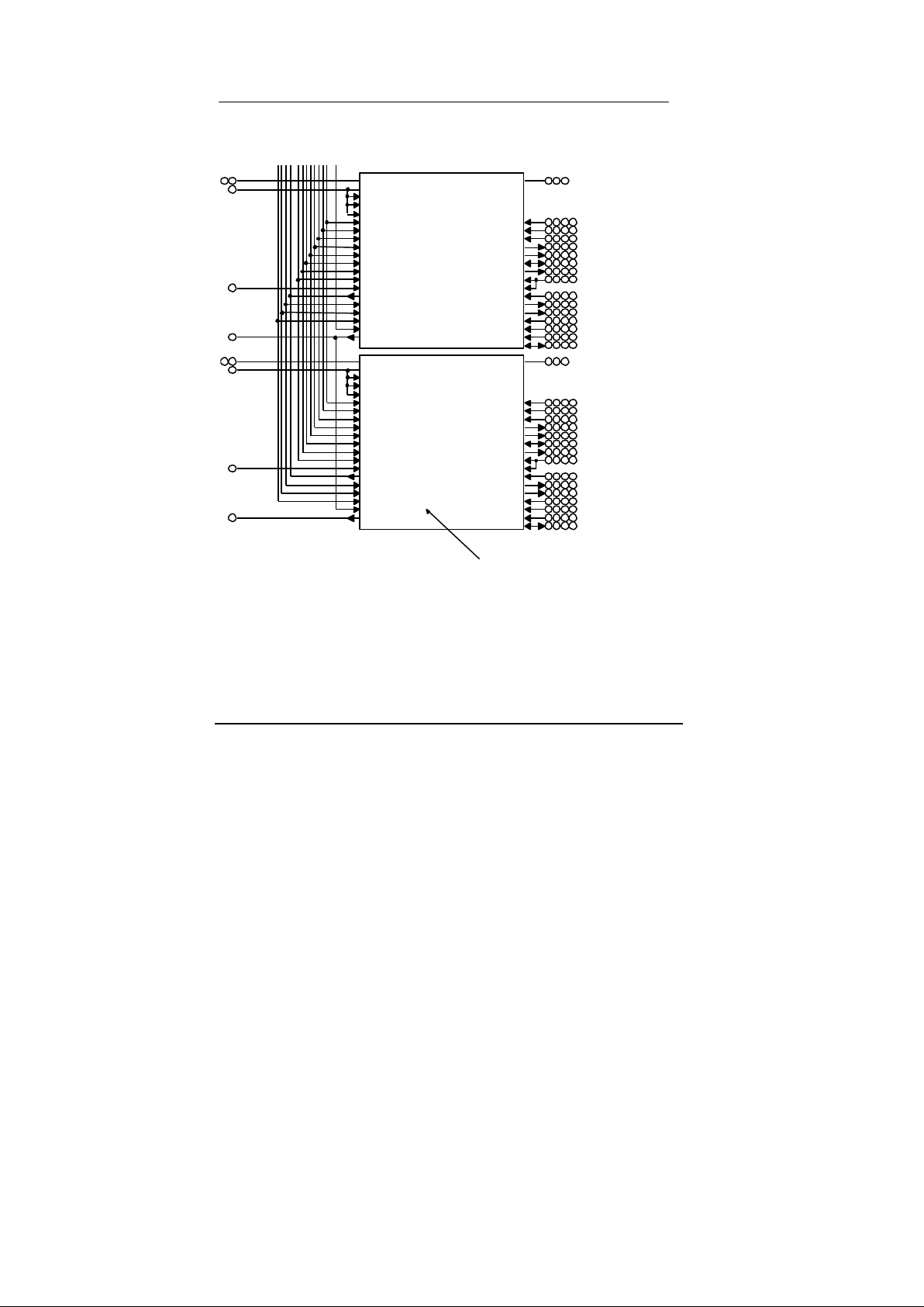
1. MULTI-CHIP MODULE (MCM) DESCRIPTION
The Four x Four and Four x Three MCMs offer a high density packaging arrangement for
the DS21Q44 E1 Enhanced Quad Framer. Either three (DS21FT44) or four (DS21FF44)
silicon die of these devices is packaged in a Multi-Chip Module (MCM) with the electrical
connections as shown in Figure 1-1.
All of the functions available on the DS21Q44 are also available in the MCM packaged
version. However, in order to minimize package size, some signals have been deleted or
combined. These differences are detailed in Table 1-1. In the Four x Three (FT) version,
the fourth quad framer is not populated and hence all of the signals to and from this fourth
framer are absent and should be treated as No Connects (NC). Table 2-1 lists all of the
signals on the MCM and it also lists the absent signals for the Four x Three.
The availability of both a twelve and a sixteen channel version allow the maximum framer
density with the lowest cost.

DALLAS
SEMICONDUCTOR DS21FT44 / DS21FF44
4 X 3 Twelve Channel E1 Framer
4 X 4 Sixteen Channel E1 Framer
101899 2/119
Changes from Normal DS21Q44 Configuration Table 1-1
1. TSYSCLK and RSYSCLK are tied together.
2. The following signals are not available:
RFSYNC / RLCLK / RLINK / RCHCLK / RMSYNC / RLOS/LOTC /
TCHBLK / TLCLK / TLINK / TCHCLK
DS21FT44 / DS21FF44 Schematic Figure 1-1
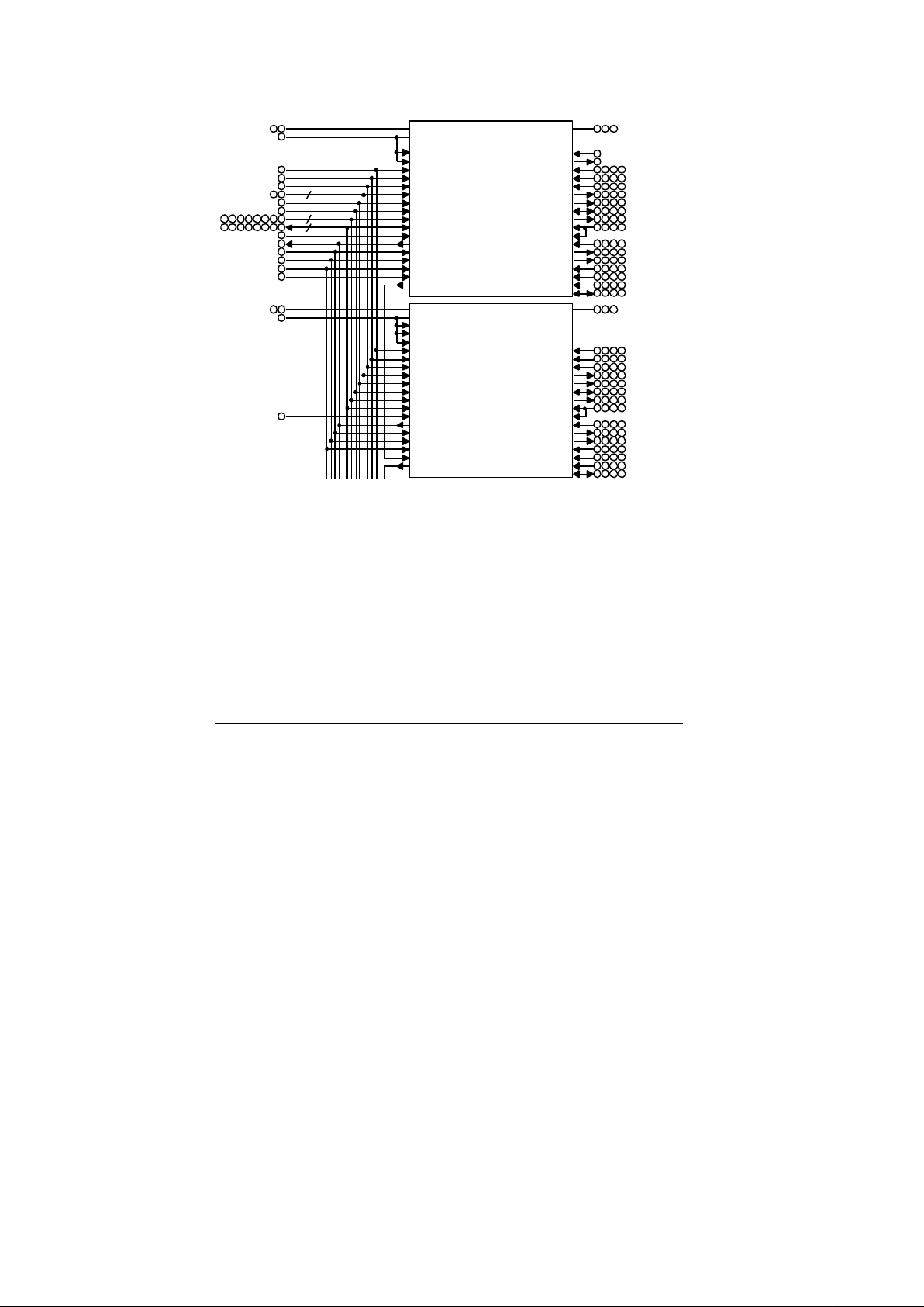
DALLAS SEMICONDUCTOR DS21FF44/DS21FT44
101899 3/119
8MCLK
CLKSI
RCLK1/2/3/4
RPOS1/2/3/4
RNEG1/2/3/4
RSER1/2/3/4
RSIG1/2/3/4
RSYNC1/2/3/4
RSYSCLK1/2/3/4
TCLK1/2/3/4
TNEG1/2/3/4
TPOS1/2/3/4
TSER1/2/3/4
TSIG1/2/3/4
TSSYNC1/2/3/4
TSYNC1/2/3/4
TSYSCLK1/2/3/4
TLINK0/1/2/3
JTDO
JTDI
JTCLK
JTMS
JTRST
INT*
FMS
D0 to D7
A0 to A7
RD*
WR*
BTS
MUX
CS*
FS0/FS1
TEST
Signals Not Connected &
Left Open Circuited Include:
RLOS/LOTC
RLINK
RLCLK
RCHCLK
RMSYNC
RFSYNC
TLCLK
TCHCLK
TCHBLK
DS21Q44 # 1
RCLK5/6/7/8
RPOS5/6/7/8
RNEG5/6/7/8
RSER5/6/7/8
RSIG5/6/7/8
RSYNC5/6/7/8
RSYSCLK5/6/7/8
TCLK5/6/7/8
TNEG5/6/7/8
TPOS5/6/7/8
TSER5/6/7/8
TSIG5/6/7/8
TSSYNC5/6/7/8
TSYNC5/6/7/8
TSYSCLK5/6/7/8
JTDO
JTDI
JTCLK
JTMS
JTRST
INT*
D0 to D7
A0 to A7
RD*
WR*
BTS
MUX
CS*
FS0/FS1
TEST
Signals Not Connected &
Left Open Circuited Include:
RLOS/LOTC
RLINK
RLCLK
RCHCLK
RMSYNC
RFSYNC
TLCLK
TCHCLK
TCHBLK
8MCLK
DS21Q44 # 2
2
8
8
See Connecting Page
RCHBLK5/6/7/8
RCHBLK1/2/3/4
DVDD
DVSS
DVSS
TLINK0/1/2/3
FMS
CLKSI
DVSS
DVSS
DVDD
DALLAS SEMICONDUCTOR DS21FF44/DS21FT44
101899 4/119
DS21FF44 / DS21FT44 Schematic Figure 1-1 (continued)
CLKSI
RCLK9/10/11/12
RPOS9/10/11/12
RNEG9/10/11/12
RSER9/10/11/12
RSIG9/10/11/12
RSYNC9/10/11/12
RSYSCLK9/10/11/12
TCLK9/10/11/12
TNEG9/10/11/12
TPOS9/10/11/12
TSER9/10/11/12
TSIG9/10/11/12
TSSYNC9/10/11/12
TSYNC9/10/11/12
TSYSCLK9/10/11/12
TLINK0/1/2/3
JTDO
JTDI
JTCLK
JTMS
JTRST
INT*
FMS
D0 to D7
A0 to A7
RD*
WR*
BTS
MUX
CS*
FS0/FS1
TEST
Signals Not Connected &
Left Open Circuited Include:
RLOS/LOTC
RLINK
RLCLK
RCHCLK
RMSYNC
RFSYNC
TLCLK
TCHCLK
TCHBLK
8MCLK
DS21Q44 # 3
RCLK13/14/15/16
RPOS13/14/15/16
RNEG13/14/15/16
RSER13/14/15/16
RSIG13/14/15/16
RSYNC13/14/15/16
RSYSCLK13/14/15/16
TCLK13/14/15/16
TNEG13/14/15/16
TPOS13/14/15/16
TSER13/14/15/16
TSIG13/14/15/16
TSSYNC13/14/15/16
TSYNC13/14/15/16
TSYSCLK13/14/15/16
JTDO
JTDI
JTCLK
JTMS
JTRST
INT*
D0 to D7
A0 to A7
RD*
WR*
BTS
MUX
CS*
FS0/FS1
TEST
Signals Not Connected &
Left Open Circuited Include:
RLOS/LOTC
RLINK
RLCLK
RCHCLK
RMSYNC
RFSYNC
TLCLK
TCHCLK
TCHBLK
8MCLK
DS21Q44 # 4
RCHBLK13/14/15/16
RCHBLK9/10/11/12
DVDD
DVSS
DVSS
TLINK0/1/2/3
FMS
CLKSI
DVSS
DVSS
DVDD
See Connecting Page
jtdot
jtdof
The Fourth Quad Framer
is Not Populated
on the 12 Channel
DS21FT44

DALLAS SEMICONDUCTOR DS21FF44/DS21FT44
101899 5/119
TABLE OF CONTENTS
1. MULTI-CHIP MODULE (MCM) DESCRIPTION.................................... 1
2. MCM LEAD DESCRIPTION................................ ................................ . 7
3. DS21FF44 (FOUR X FOUR) PCB LAND PATTERNS .............................12
4. DS21FT44 (FOUR X THREE) PCB LAND PATTERN ............................ 13
5. DS21Q42 DIE DESCRIPTION ................................ .............................. 14
6. DS21Q44 INTRODUCTION ................................ .................................15
7. DS21Q44 PIN FUNCTION DESCRIPTION ...........................................19
8. DS21Q44 REGISTER MAP.................................................................. 28
9. PARALLEL PORT ................................ ................................ ..............33
10. CONTROL, ID AND TEST REGISTERS ...........................................33
11. STATUS AND INFORMATION REGISTERS .....................................43
12. ERROR COUNT REGISTERS ................................ ........................... 50
13. DS0 MONITORING FUNCTION........................................................ 53
14. SIGNALING OPERATION................................................................56
14.1 PROCESSOR BASED SIGNALING..............................................................................................56
14.2 HARDWARE BASED SIGNALING.............................................................................................59
15. PER–CHANNEL CODE GENERATION AND LOOPBACK ................62
15.1 TRANSMIT SIDE CODE GENERATION....................................................................................62
15.1.1 Simple Idle Code Insertion and Per–Channel Loopback .......................................................62
15.1.2 Per–Channel Code Insertion ...................................................................................................63
15.2 RECEIVE SIDE CODE GENERATION .......................................................................................64
16. CLOCK BLOCKING REGISTERS ................................ .................... 66
17. ELASTIC STORES OPERATION .....................................................68
17.1 RECEIVE SIDE...............................................................................................................................68
17.2 TRANSMIT SIDE...........................................................................................................................69
18. ADDITIONAL (SA) AND INTERNATIONAL (SI) BIT OPERATION ...70
18.1 HARDWARE SCHEME .................................................................................................................70
18.2 INTERNAL REGISTER SCHEME BASED ON DOUBLE–FRAME ..........................................70

DALLAS SEMICONDUCTOR DS21FF44/DS21FT44
101899 6/119
18.3 INTERNAL REGISTER SCHEME BASED ON CRC4 MULTIFRAME .....................................72
19. HDLC CONTROLLER FOR THE SA BITS OR DS0 .......................... 75
19.1 GENERAL OVERVIEW.........................................................................................................................75
19.2 HDLC STATUS REGISTERS.................................................................................................................76
19.3 BASIC OPERATION D ETAILS................................................................................................................76
19.4 HDLC REGISTER DESCRIPTION..........................................................................................................77
20. INTERLEAVED PCM BUS OPERATION ..........................................85
21. JTAG-BOUNDARY SCAN ARCHITECTURE AND TEST ACCESS PORT
88
21.1 DESCRIPTION......................................................................................................................................88
21.2 TAP CONTROLLER STATE MACHINE ..................................................................................................90
21.3 INSTRUCTION REGISTER AND INSTRUCTIONS........................................................................................93
21.4 TEST REGISTERS ................................................................................................................................95
22. TIMING DIAGRAMS ......................................................................100
23. OPERATING PARAMETERS..........................................................115
24. MCM PACKAGE DIMENSIONS...................................................... 132
DOCUMENT REVISION HISTORY
Revision Notes
8-7-98 Initial Release
12-29-98 TEST and MUX leads were added at previous No Connect (NC) leads.
10-18-99 DS21Q42 die specifications appended to data sheet.
DALLAS SEMICONDUCTOR DS21FF44/DS21FT44
101899 7/119
2. MCM LEAD DESCRIPTION
Lead Description Sorted by Symbol Table 2-1
Lead Symbol I/O Description
B7 8MCLK O 8.192 MHz Clock Based on CLKSI.
G20 A0 I Address Bus Bit 0 (lsb).
H20 A1 I Address Bus Bit 1.
G19 A2 I Address Bus Bit 2.
H19 A3 I Address Bus Bit 3.
G18 A4 I Address Bus Bit 4.
H18 A5 I Address Bus Bit 5.
G17 A6 I Address Bus Bit 6.
H17 A7 I Address Bus Bit 7 (msb).
W15 BTS I Bus Timing Select. 0 = Intel / 1 = Motorola.
B6 CLKSI I Reference clock for the 8.192MHz clock synthesizer.
T8 CS1* I Chip Select for Quad Framer 1.
Y4 CS2* I Chip Select for Quad Framer 2.
Y15 CS3* I Chip Select for Quad Framer 3.
E19 CS4*/NC I Chip Select for Quad Framer 4. NC on Four x Three.
L20 D0 I/O Data Bus Bit 0 (lsb).
M20 D1 I/O Data Bus Bit 1.
L19 D2 I/O Data Bus Bit 2.
M19 D3 I/O Data Bus Bit 3.
L18 D4 I/O Data Bus Bit 4.
M18 D5 I/O Data Bus Bit 5.
L17 D6 I/O Data Bus Bit 6.
M17 D7 I/O Data Bus Bit 7 (msb).
C7 DVDD1 – Digital Positive Supply for Framer 1.
E4 DVDD1 – Digital Positive Supply for Framer 1.
D2 DVDD1 – Digital Positive Supply for Framer 1.
K3 DVDD2 – Digital Positive Supply for Framer 2.
U7 DVDD2 – Digital Positive Supply for Framer 2.
P2 DVDD2 – Digital Positive Supply for Framer 2.
V19 DVDD3 – Digital Positive Supply for Framer 3.
T12 DVDD3 – Digital Positive Supply for Framer 3.
L16 DVDD3 – Digital Positive Supply for Framer 3.
D17 DVDD4/NC – Digital Positive Supply for Framer 4. NC on Four x Three.
F16 DVDD4/NC – Digital Positive Supply for Framer 4. NC on Four x Three.
B11 DVDD4/NC – Digital Positive Supply for Framer 4. NC on Four x Three.
E9 DVSS1 – Digital Signal Ground for Framer 1.
A6 DVSS1 – Digital Signal Ground for Framer 1.
D5 DVSS1 – Digital Signal Ground for Framer 1.
U3 DVSS2 – Digital Signal Ground for Framer 2.
K4 DVSS2 – Digital Signal Ground for Framer 2.
U8 DVSS2 – Digital Signal Ground for Framer 2.
U4 DVSS3 – Digital Signal Ground for Framer 3.
R16 DVSS3 – Digital Signal Ground for Framer 3.
Y20 DVSS3 – Digital Signal Ground for Framer 3.
J20 DVSS4/NC – Digital Signal Ground for Framer 4. NC on Four x Three.
A11 DVSS4/NC – Digital Signal Ground for Framer 4. NC on Four x Three.
D19 DVSS4/NC – Digital Signal Ground for Framer 4. NC on Four x Three.
Y14 FS0 I Framer Select 0 for the Parallel Control Port.
W14 FS1 I Framer Select 1 for the Parallel Control Port.
G16 INT* O Interrupt for all four Quad Framers.
V14 JTCLK I JTAG Clock.
E10 JTDI I JTAG Data Input.
A19 JTDOF/NC O JTAG Data Output for Four x Four Version. NC on Four x Three.
T17 JTDOT O JTAG Data Output for Four x Three Version.
H16 JTMS I JTAG Test Mode Select.
K17 JTRST* I JTAG Reset.
A13 TEST I Tri-State. 0 = do not tri-state / 1 = tri-state all outputs & I/O signals
P17 MUX I Bus Operation Select. 0 = non-multiplexed bus / 1 = multiplexed bus

DALLAS SEMICONDUCTOR DS21FF44/DS21FT44
101899 8/119
C2 RCHBLK1 O Receive Channel Blocking Clock.
G3 RCHBLK2 O Receive Channel Blocking Clock.
E6 RCHBLK3 O Receive Channel Blocking Clock.
A8 RCHBLK4 O Receive Channel Blocking Clock.
N1 RCHBLK5 O Receive Channel Blocking Clock.
Y1 RCHBLK6 O Receive Channel Blocking Clock.
U6 RCHBLK7 O Receive Channel Blocking Clock.
N5 RCHBLK8 O Receive Channel Blocking Clock.
Y8 RCHBLK9 O Receive Channel Blocking Clock.
W12 RCHBLK10 O Receive Channel Blocking Clock.
V17 RCHBLK11 O Receive Channel Blocking Clock.
U17 RCHBLK12 O Receive Channel Blocking Clock.
D16 RCHBLK13/NC O Receive Channel Blocking Clock. NC on Four x Three.
K20 RCHBLK14/NC O Receive Channel Blocking Clock. NC on Four x Three.
B18 RCHBLK15/NC O Receive Channel Blocking Clock. NC on Four x Three.
B16 RCHBLK16/NC O Receive Channel Blocking Clock. NC on Four x Three.
A2 RCLK1 I Receive Clock for Framer 1
K1 RCLK2 I Receive Clock for Framer 2.
D10 RCLK3 I Receive Clock for Framer 3.
B9 RCLK4 I Receive Clock for Framer 4.
M3 RCLK5 I Receive Clock for Framer 5.
V1 RCLK6 I Receive Clock for Framer 6.
W6 RCLK7 I Receive Clock for Framer 7.
J3 RCLK8 I Receive Clock for Framer 8.
T9 RCLK9 I Receive Clock for Framer 9.
W10 RCLK10 I Receive Clock for Framer 10.
Y18 RCLK11 I Receive Clock for Framer 11.
N17 RCLK12 I Receive Clock for Framer 12.
D14 RCLK13/NC I Receive Clock for Framer 13. NC on Four x Three.
P20 RCLK14/NC I Receive Clock for Framer 14. NC on Four x Three.
C18 RCLK15/NC I Receive Clock for Framer 15. NC on Four x Three.
C12 RCLK16/NC I Receive Clock for Framer 16. NC on Four x Three.
E18 RD* I Read Input.
B2 RNEG1 I Receive Negative Data for Framer 1.
H2 RNEG2 I Receive Negative Data for Framer 2.
D9 RNEG3 I Receive Negative Data for Framer 3.
A9 RNEG4 I Receive Negative Data for Framer 4.
M2 RNEG5 I Receive Negative Data for Framer 5.
V3 RNEG6 I Receive Negative Data for Framer 6.
V7 RNEG7 I Receive Negative Data for Framer 7.
P3 RNEG8 I Receive Negative Data for Framer 8.
U9 RNEG9 I Receive Negative Data for Framer 9.
W11 RNEG10 I Receive Negative Data for Framer 10.
W17 RNEG11 I Receive Negative Data for Framer 11.
T20 RNEG12 I Receive Negative Data for Framer 12.
E14 RNEG13/NC I Receive Negative Data for Framer 13. NC on Four x Three.
N20 RNEG14/NC I Receive Negative Data for Framer 14. NC on Four x Three.
C20 RNEG15/NC I Receive Negative Data for Framer 15. NC on Four x Three.
B13 RNEG16/NC I Receive Negative Data for Framer 16. NC on Four x Three.
A1 RPOS1 I Receive Positive Data for Framer 1.
H1 RPOS2 I Receive Positive Data for Framer 2.
H4 RPOS3 I Receive Positive Data for Framer 3.
C9 RPOS4 I Receive Positive Data for Framer 4.
M1 RPOS5 I Receive Positive Data for Framer 5.
W2 RPOS6 I Receive Positive Data for Framer 6.
V5 RPOS7 I Receive Positive Data for Framer 7.
P4 RPOS8 I Receive Positive Data for Framer 8.
T10 RPOS9 I Receive Positive Data for Framer 9.
V11 RPOS10 I Receive Positive Data for Framer 10.
Y19 RPOS11 I Receive Positive Data for Framer 11.
R19 RPOS12 I Receive Positive Data for Framer 12.
D15 RPOS13/NC I Receive Positive Data for Framer 13. NC on Four x Three.
J18 RPOS14/NC I Receive Positive Data for Framer 14. NC on Four x Three.
A20 RPOS15/NC I Receive Positive Data for Framer 15. NC on Four x Three.
A14 RPOS16/NC I Receive Positive Data for Framer 16. NC on Four x Three.
DALLAS SEMICONDUCTOR DS21FF44/DS21FT44
101899 9/119
C1 RSER1 O Receive Serial Data from Framer 1.
H3 RSER2 O Receive Serial Data from Framer 2.
C6 RSER3 O Receive Serial Data from Framer 3.
C8 RSER4 O Receive Serial Data from Framer 4.
P1 RSER5 O Receive Serial Data from Framer 5.
W4 RSER6 O Receive Serial Data from Framer 6.
T7 RSER7 O Receive Serial Data from Framer 7.
N4 RSER8 O Receive Serial Data from Framer 8.
U11 RSER9 O Receive Serial Data from Framer 9.
Y12 RSER10 O Receive Serial Data from Framer 10.
V16 RSER11 O Receive Serial Data from Framer 11.
T16 RSER12 O Receive Serial Data from Framer 12.
E16 RSER13/NC O Receive Serial Data from Framer 13. NC on Four x Three.
F20 RSER14/NC O Receive Serial Data from Framer 14. NC on Four x Three.
C16 RSER15/NC O Receive Serial Data from Framer 15. NC on Four x Three.
A12 RSER16/NC O Receive Serial Data from Framer 16. NC on Four x Three.
D3 RSIG1 O Receive Signaling Output from Framer 1.
G2 RSIG2 O Receive Signaling Output from Framer 2.
D4 RSIG3 O Receive Signaling Output from Framer 3.
D8 RSIG4 O Receive Signaling Output from Framer 4.
N2 RSIG5 O Receive Signaling Output from Framer 5.
V4 RSIG6 O Receive Signaling Output from Framer 6.
V6 RSIG7 O Receive Signaling Output from Framer 7.
K5 RSIG8 O Receive Signaling Output from Framer 8.
U10 RSIG9 O Receive Signaling Output from Framer 9.
Y11 RSIG10 O Receive Signaling Output from Framer 10.
W19 RSIG11 O Receive Signaling Output from Framer 11.
U20 RSIG12 O Receive Signaling Output from Framer 12.
E15 RSIG13/NC O Receive Signaling Output from Framer 13. NC on Four x Three.
K19 RSIG14/NC O Receive Signaling Output from Framer 14. NC on Four x Three.
C17 RSIG15/NC O Receive Signaling Output from Framer 15. NC on Four x Three.
A15 RSIG16/NC O Receive Signaling Output from Framer 16. NC on Four x Three.
B1 RSYNC1 I/O Receive Frame/Multiframe Sync for Framer 1.
G1 RSYNC2 I/O Receive Frame/Multiframe Sync for Framer 2.
D6 RSYNC3 I/O Receive Frame/Multiframe Sync for Framer 3.
A7 RSYNC4 I/O Receive Frame/Multiframe Sync for Framer 4.
N3 RSYNC5 I/O Receive Frame/Multiframe Sync for Framer 5.
Y2 RSYNC6 I/O Receive Frame/Multiframe Sync for Framer 6.
U5 RSYNC7 I/O Receive Frame/Multiframe Sync for Framer 7.
J4 RSYNC8 I/O Receive Frame/Multiframe Sync for Framer 8.
T11 RSYNC9 I/O Receive Frame/Multiframe Sync for Framer 9.
V13 RSYNC10 I/O Receive Frame/Multiframe Sync for Framer 10.
V15 RSYNC11 I/O Receive Frame/Multiframe Sync for Framer 11.
P18 RSYNC12 I/O Receive Frame/Multiframe Sync for Framer 12.
J17 RSYNC13/NC I/O Receive Frame/Multiframe Sync for Framer 13. NC on Four x Three.
J19 RSYNC14/NC I/O Receive Frame/Multiframe Sync for Framer 14. NC on Four x Three.
B17 RSYNC15/NC I/O Receive Frame/Multiframe Sync for Framer 15. NC on Four x Three.
B12 RSYNC16/NC I/O Receive Frame/Multiframe Sync for Framer 16. NC on Four x Three.
B5 SYSCLK1 I System Clock for Framer 1.
E2 SYSCLK2 I System Clock for Framer 2.
E5 SYSCLK3 I System Clock for Framer 3.
B8 SYSCLK4 I System Clock for Framer 4.
M4 SYSCLK5 I System Clock for Framer 5.
T2 SYSCLK6 I System Clock for Framer 6.
Y5 SYSCLK7 I System Clock for Framer 7.
W3 SYSCLK8 I System Clock for Framer 8.
T4 SYSCLK9 I System Clock for Framer 9.
Y9 SYSCLK10 I System Clock for Framer 10.
U12 SYSCLK11 I System Clock for Framer 11.
R17 SYSCLK12 I System Clock for Framer 12.
E13 SYSCLK13/NC I System Clock for Framer 13. NC on Four x Three.
N18 SYSCLK14/NC I System Clock for Framer 14. NC on Four x Three.
E20 SYSCLK15/NC I System Clock for Framer 15. NC on Four x Three.
C14 SYSCLK16/NC I System Clock for Framer 16. NC on Four x Three.
D1 TCLK1 I Transmit Clock for Framer 1.

DALLAS SEMICONDUCTOR DS21FF44/DS21FT44
101899 10/119
H5 TCLK2 I Transmit Clock for Framer 2.
C5 TCLK3 I Transmit Clock for Framer 3.
A5 TCLK4 I Transmit Clock for Framer 4.
R1 TCLK5 I Transmit Clock for Framer 5.
Y3 TCLK6 I Transmit Clock for Framer 6.
T6 TCLK7 I Transmit Clock for Framer 7.
K2 TCLK8 I Transmit Clock for Framer 8.
U13 TCLK9 I Transmit Clock for Framer 9.
Y13 TCLK10 I Transmit Clock for Framer 10.
T18 TCLK11 I Transmit Clock for Framer 11.
P16 TCLK12 I Transmit Clock for Framer 12.
K16 TCLK13/NC I Transmit Clock for Framer 13. NC on Four x Three.
F19 TCLK14/NC I Transmit Clock for Framer 14. NC on Four x Three.
E17 TCLK15/NC I Transmit Clock for Framer 15. NC on Four x Three.
C11 TCLK16/NC I Transmit Clock for Framer 16. NC on Four x Three.
C3 TNEG1 O Transmit Negative Data from Framer 1.
J1 TNEG2 O Transmit Negative Data from Framer 2.
F5 TNEG3 O Transmit Negative Data from Framer 3.
A10 TNEG4 O Transmit Negative Data from Framer 4.
L1 TNEG5 O Transmit Negative Data from Framer 5.
V2 TNEG6 O Transmit Negative Data from Framer 6.
V8 TNEG7 O Transmit Negative Data from Framer 7.
P5 TNEG8 O Transmit Negative Data from Framer 8.
U14 TNEG9 O Transmit Negative Data from Framer 9.
V12 TNEG10 O Transmit Negative Data from Framer 10.
W18 TNEG11 O Transmit Negative Data from Framer 11.
T19 TNEG12 O Transmit Negative Data from Framer 12.
D11 TNEG13/NC O Transmit Negative Data from Framer 13. NC on Four x Three.
K18 TNEG14/NC O Transmit Negative Data from Framer 14. NC on Four x Three.
C19 TNEG15/NC O Transmit Negative Data from Framer 15. NC on Four x Three.
B15 TNEG16/NC O Transmit Negative Data from Framer 16. NC on Four x Three.
B3 TPOS1 O Transmit Positive Data from Framer 1.
J2 TPOS2 O Transmit Positive Data from Framer 2.
J5 TPOS3 O Transmit Positive Data from Framer 3.
B10 TPOS4 O Transmit Positive Data from Framer 4.
L2 TPOS5 O Transmit Positive Data from Framer 5.
W1 TPOS6 O Transmit Positive Data from Framer 6.
W7 TPOS7 O Transmit Positive Data from Framer 7.
R3 TPOS8 O Transmit Positive Data from Framer 8.
T14 TPOS9 O Transmit Positive Data from Framer 9.
Y10 TPOS10 O Transmit Positive Data from Framer 10.
V18 TPOS11 O Transmit Positive Data from Framer 11.
V20 TPOS12 O Transmit Positive Data from Framer 12.
E12 TPOS13/NC O Transmit Positive Data from Framer 13. NC on Four x Three.
N19 TPOS14/NC O Transmit Positive Data from Framer 14. NC on Four x Three.
B19 TPOS15/NC O Transmit Positive Data from Framer 15. NC on Four x Three.
B14 TPOS16/NC O Transmit Positive Data from Framer 16. NC on Four x Three.
B4 TSER1 I Transmit Serial Data for Framer 1.
E1 TSER2 I Transmit Serial Data for Framer 2.
F3 TSER3 I Transmit Serial Data for Framer 3.
D7 TSER4 I Transmit Serial Data for Framer 4.
L5 TSER5 I Transmit Serial Data for Framer 5.
T1 TSER6 I Transmit Serial Data for Framer 6.
Y6 TSER7 I Transmit Serial Data for Framer 7.
T3 TSER8 I Transmit Serial Data for Framer 8.
M16 TSER9 I Transmit Serial Data for Framer 9.
W9 TSER10 I Transmit Serial Data for Framer 10.
W16 TSER11 I Transmit Serial Data for Framer 11.
W20 TSER12 I Transmit Serial Data for Framer 12.
D13 TSER13/NC I Transmit Serial Data for Framer 13. NC on Four x Three.
F17 TSER14/NC I Transmit Serial Data for Framer 14. NC on Four x Three.
D18 TSER15/NC I Transmit Serial Data for Framer 15. NC on Four x Three.
A18 TSER16/NC I Transmit Serial Data for Framer 16. NC on Four x Three.
C4 TSIG1 I Transmit Signaling Input for Framer 1.
F1 TSIG2 I Transmit Signaling Input for Framer 2.
DALLAS SEMICONDUCTOR DS21FF44/DS21FT44
101899 11/119
G4 TSIG3 I Transmit Signaling Input for Framer 3.
C10 TSIG4 I Transmit Signaling Input for Framer 4.
L3 TSIG5 I Transmit Signaling Input for Framer 5.
U2 TSIG6 I Transmit Signaling Input for Framer 6.
V9 TSIG7 I Transmit Signaling Input for Framer 7.
R5 TSIG8 I Transmit Signaling Input for Framer 8.
U15 TSIG9 I Transmit Signaling Input for Framer 9.
V10 TSIG10 I Transmit Signaling Input for Framer 10.
U18 TSIG11 I Transmit Signaling Input for Framer 11.
R18 TSIG12 I Transmit Signaling Input for Framer 12.
E11 TSIG13/NC I Transmit Signaling Input for Framer 13. NC on Four x Three.
P19 TSIG14/NC I Transmit Signaling Input for Framer 14. NC on Four x Three.
B20 TSIG15/NC I Transmit Signaling Input for Framer 15. NC on Four x Three.
A16 TSIG16/NC I Transmit Signaling Input for Framer 16. NC on Four x Three.
A3 TSSYNC1 I Transmit System Sync for Framer 1.
F2 TSSYNC2 I Transmit System Sync for Framer 2.
G5 TSSYNC3 I Transmit System Sync for Framer 3.
E8 TSSYNC4 I Transmit System Sync for Framer 4.
L4 TSSYNC5 I Transmit System Sync for Framer 5.
U1 TSSYNC6 I Transmit System Sync for Framer 6.
Y7 TSSYNC7 I Transmit System Sync for Framer 7.
R4 TSSYNC8 I Transmit System Sync for Framer 8.
T15 TSSYNC9 I Transmit System Sync for Framer 9.
W8 TSSYNC10 I Transmit System Sync for Framer 10.
Y17 TSSYNC11 I Transmit System Sync for Framer 11.
U19 TSSYNC12 I Transmit System Sync for Framer 12.
C13 TSSYNC13/NC I Transmit System Sync for Framer 13. NC on Four x Three.
R20 TSSYNC14/NC I Transmit System Sync for Framer 14. NC on Four x Three.
D20 TSSYNC15/NC I Transmit System Sync for Framer 15. NC on Four x Three.
A17 TSSYNC16/NC I Transmit System Sync for Framer 16. NC on Four x Three.
E3 TSYNC1 I/O Transmit Sync for Framer 1.
F4 TSYNC2 I/O Transmit Sync for Framer 2.
E7 TSYNC3 I/O Transmit Sync for Framer 3.
A4 TSYNC4 I/O Transmit Sync for Framer 4.
R2 TSYNC5 I/O Transmit Sync for Framer 5.
W5 TSYNC6 I/O Transmit Sync for Framer 6.
T5 TSYNC7 I/O Transmit Sync for Framer 7.
M5 TSYNC8 I/O Transmit Sync for Framer 8.
T13 TSYNC9 I/O Transmit Sync for Framer 9.
W13 TSYNC10 I/O Transmit Sync for Framer 10.
U16 TSYNC11 I/O Transmit Sync for Framer 11.
N16 TSYNC12 I/O Transmit Sync for Framer 12.
J16 TSYNC13/NC I/O Transmit Sync for Framer 13. NC on Four x Three.
F18 TSYNC14/NC I/O Transmit Sync for Framer 14. NC on Four x Three.
C15 TSYNC15/NC I/O Transmit Sync for Framer 15. NC on Four x Three.
D12 TSYNC16/NC I/O Transmit Sync for Framer 16. NC on Four x Three.
Y16 WR* I Write Input.

DALLAS SEMICONDUCTOR DS21FF44/DS21FT44
101899 12/119
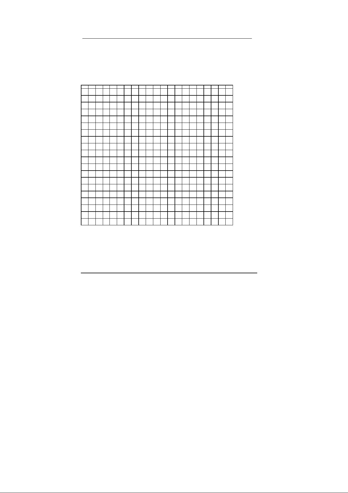
3. DS21FF44 (Four x Four) PCB LAND PATTERNS
Figure 3-1
The diagram shown below is the lead pattern that will be placed on the target PCB. This is
the same pattern that would be seen as viewed through the MCM from the top.
1 2 3 4 5 6 7 8 9 10 11 12 13 14 15 16 17 18 19 20
A
rpos1rclk1ts
sync
1
tsyn
c
4
tclk4dvss1rsyn
c
4
rch
blk
4
rneg4tneg4dvss4rser16test rpos16rsig16tsig16ts
sync
16
tser16jtdof rpos
15
B
rsyn
c
1
rneg1tpos1tser1sys
clk
1
clksi 8
mclk
sys
clk
4
rclk4tpos4dvdd4rsyn
c
16
rneg16tpos16tneg16rch
blk
16
rsyn
c
15
rch
blk
15
tpos15tsig
15
C
rser1rch
blk
1
tneg1tsig1tclk3rser3dvdd1rser4 rpos4tsig4tclk16rclk16ts
sync
13
sys
clk
16
tsyn
c
15
rser15rsig15rclk15tneg15rneg
15
D
tclk1dvdd1rsig1rsig3dvss1rsyn
c
3
tser4rsig4 rneg3rclk3tneg13tsyn
c
16
tser13rclk13rpos13rch
blk
13
dvdd4tser15dvss4ts
sync
15
E
tser2sys
clk
2
tsyn
c
1
dvdd1sys
clk
3
rch
blk
3
tsyn
c
3
ts
sync
4
dvss1jtdi tsig13tpos13sys
clk
13
rneg13rsig13rser13tclk15rd* cs4* sys
clk
15
F
tsig2ts
sync
2
tser3tsyn
c
2
tneg
3
dvdd4tser14tsyn
c
14
tclk14rser
14
G
rsyn
c
2
rsig2rch
blk
2
tsig3ts
sync
3
int* A6 A4 A2 A0
H
rpos2rneg2rser2rpos3tclk
2
jtms A7 A5 A3 A1
J
tneg2tpos2rclk8rsyn
c
8
tpos
3
tsyn
c
13
rsyn
c
13
rpos14rsyn
c
14
dvss
4
K
rclk2tclk8dvdd2dvss2rsig
8
tclk13jtrst* tneg14rsig14rch
blk
14
L
tneg5tpos5tsig5ts
sync
5
tser
5
dvdd3D6 D4 D2 D0
M
rpos5rneg5rclk5sys
clk
5
tsyn
c
8
tser9D7 D5 D3 D1
N
rch
blk
5
rsig5rsyn
c
5
rser8rch
blk
8
tsyn
c
12
rclk12sys
clk
14
tpos14rneg
14
P
rser5dvdd2rneg8rpos8tneg
8
tclk12mux rsyn
c
12
tsig14rclk
14
R
tclk5tsyn
c
5
tpos8ts
sync
8
tsig
8
dvss3sys
clk
12
tsig12rpos12ts
sync
14
T
tser6sys
clk
6
tser8sys
clk
9
tsyn
c
7
tclk7rser7cs1* rclk9rpos9rsyn
c
9
dvdd3tsyn
c
9
tpos9ts
sync
9
rser12jtdot tclk11tneg12rneg
12
U
ts
sync
6
tsig6dvss2dvss3rsyn
c
7
rch
blk
7
dvdd2dvss2rneg9rsig9rser9sys
clk
11
tclk9tneg9tsig9tsyn
c
11
rch
blk
12
tsig11tssy
nc
12
rsig
12
V
rclk6tneg6rneg6rsig6rpos7rsig7rneg7tneg7tsig7tsig10rpos10tneg10rsyn
c
10
jtclk rsyn
c
11
rser11rch
blk
11
tpos11dvdd3tpos
12
W
tpos6rpos6sys
clk
8
rser6tsyn
c
6
rclk7tpos7ts
sync
10
tser10rclk10rneg10rch
blk
10
tsyn
c
10
fs1 bts tser11rneg11tneg11rsig11tser
12
Y
rch
blk
6
rsyn
c
6
tclk6cs2* sys
clk
7
tser7ts
sync
7
rch
blk
9
sys
clk
10
tpos10rsig10rser10tclk10fs0 cs3* wr* ts
sync
11
rclk11rpos11dvss
3
DALLAS SEMICONDUCTOR DS21FF44/DS21FT44
101899 13/119
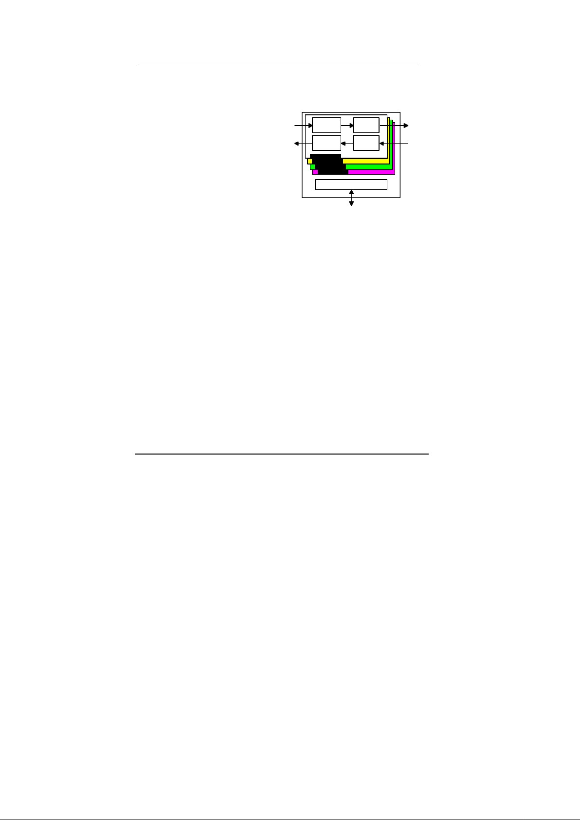
4. DS21FT44 (Four x Three) PCB Land Pattern
Figure 4-1
The diagram shown below is the lead pattern that will be placed on the target PCB. This is
the same pattern that would be seen as viewed through the MCM from the top.
1 2 3 4 5 6 7 8 9 10 11 12 13 14 15 16 17 18 19 20
A
rpos1rclk1ts
sync
1
tsyn
c
4
tclk4dvss1rsyn
c
4
rch
blk
4
rneg4tneg4nc nc test ns ns nc nc nc nc nc
B
rsyn
c
1
rneg1tpos1tser1sys
clk
1
clksi 8
mclk
sys
clk
4
rclk4tpos4nc nc nc nc nc nc nc nc nc nc
C
rser1rch
blk
1
tneg1tsig1tclk3rser3dvdd1rser4 rpos4tsig4nc nc nc nc ns nc nc nc nc nc
D
tclk1dvdd1rsig1rsig3dvss1rsyn
c
3
tser4rsig4 rneg3rclk3nc nc nc nc nc nc nc nc nc nc
E
tser2sys
clk
2
tsyn
c
1
dvdd1sys
clk
3
rch
blk
3
tsyn
c
3
ts
sync
4
dvss1jtdi nc nc nc nc nc nc nc rd* nc nc
F
tsig2ts
sync
2
tser3tsyn
c
2
tneg
3
nc nc nc nc nc
G
rsyn
c
2
rsig2rch
blk
2
tsig3ts
sync
3
int* A6 A4 A2 A0
H
rpos2rneg2rser2rpos3tclk
2
jtms A7 A5 A3 A1
J
tneg2tpos2rclk8rsyn
c
8
tpos
3
nc nc nc nc nc
K
rclk2tclk8dvdd2dvss2rsig
8
nc jtrst* nc nc nc
L
tneg5tpos5tsig5ts
sync
5
tser
5
dvdd3D6 D4 D2 D0
M
rpos5rneg5rclk5sys
clk
5
tsyn
c
8
tser9D7 D5 D3 D1
N
rch
blk
5
rsig5rsyn
c
5
rser8rch
blk
8
tsyn
c
12
rclk12nc nc nc
P
rser5dvdd2rneg8rpos8tneg
8
tclk12mux rsyn
c
12
nc nc
R
tclk5tsyn
c
5
tpos8ts
sync
8
tsig
8
dvss3sys
clk
12
tsig12rpos12nc
T
tser6sys
clk
6
tser8sys
clk
9
tsyn
c
7
tclk7rser7cs1* rclk9rpos9rsyn
c
9
dvdd3tsyn
c
9
tpos9ts
sync
9
rser12jtdot tclk11tneg12rneg
12
U
ts
sync
6
tsig6dvss2dvss3rsyn
c
7
rch
blk
7
dvdd2dvss2rneg9rsig9rser9sys
clk
11
tclk9tneg9tsig9tsyn
c
11
rch
blk
12
tsig11tssy
nc
12
rsig
12
V
rclk6tneg6rneg6rsig6rpos7rsig7rneg7tneg7tsig7tsig10rpos10tneg10rsyn
c
10
jtclk rsyn
c
11
rser11rch
blk
11
tpos11dvdd3tpos
12
W
tpos6rpos6sys
clk
8
rser6tsyn
c
6
rclk7tpos7ts
sync
10
tser10rclk10rneg10rch
blk
10
tsyn
c
10
fs1 bts tser11rneg11tneg11rsig11tser
12
Y
rch
blk
6
rsyn
c
6
tclk6cs2* sys
clk
7
tser7ts
sync
7
rch
blk
9
sys
clk
10
tpos10rsig10rser10tclk10fs0 cs3* wr* ts
sync
11
rclk11rpos11dvss
3
DALLAS SEMICONDUCTOR DS21FF44/DS21FT44
101899 14/119
5. DS21Q42 DIE DESCRIPTION
FEATURES
•
Four E1 (CEPT or PCM-30) /ISDN-PRI
framing transceivers
•
All four framers are fully independent;
transmit and receive sections of each framer
are fully independent
•
Frames to FAS, CAS, CCS, and CRC4
formats
•
Each of the four framers contain dual two–
frame elastic store slip buffers that can
connect to asynchronous backplanes up to
8.192 MHz
•
8–bit parallel control port that can be used
directly on either multiplexed or non–
multiplexed buses (Intel or Motorola)
•
Easy access to Si and Sa bits
•
Extracts and inserts CAS signaling
•
Large counters for bipolar and code
violations, CRC4 code word errors, FAS
word errors, and E-bits
•
Programmable output clocks for Fractional
E1, per channel loopback, H0 and H12
applications
•
Integral HDLC controller with 64-byte
buffers. Configurable for Sa bits or DS0
operation
•
Detects and generates AIS, remote alarm, and
remote multiframe alarms
•
Pin compatible with DS21Q42 Enhanced
Quad T1 Framer
•
3.3V supply with 5V tolerant I/O; low power
CMOS
•
Available in 128–pin TQFP package
•
IEEE 1149.1 support
FUNCTIONAL DIAGRAM
Receive
Framer
Elastic
Store
Transmit
Formatter
Elastic
Store
FRAMER #0
FRAMER #1
FRAMER #2
FRAMER #3
Control Port
DESCRIPTION

DALLAS SEMICONDUCTOR DS21FF44/DS21FT44
101899 15/119
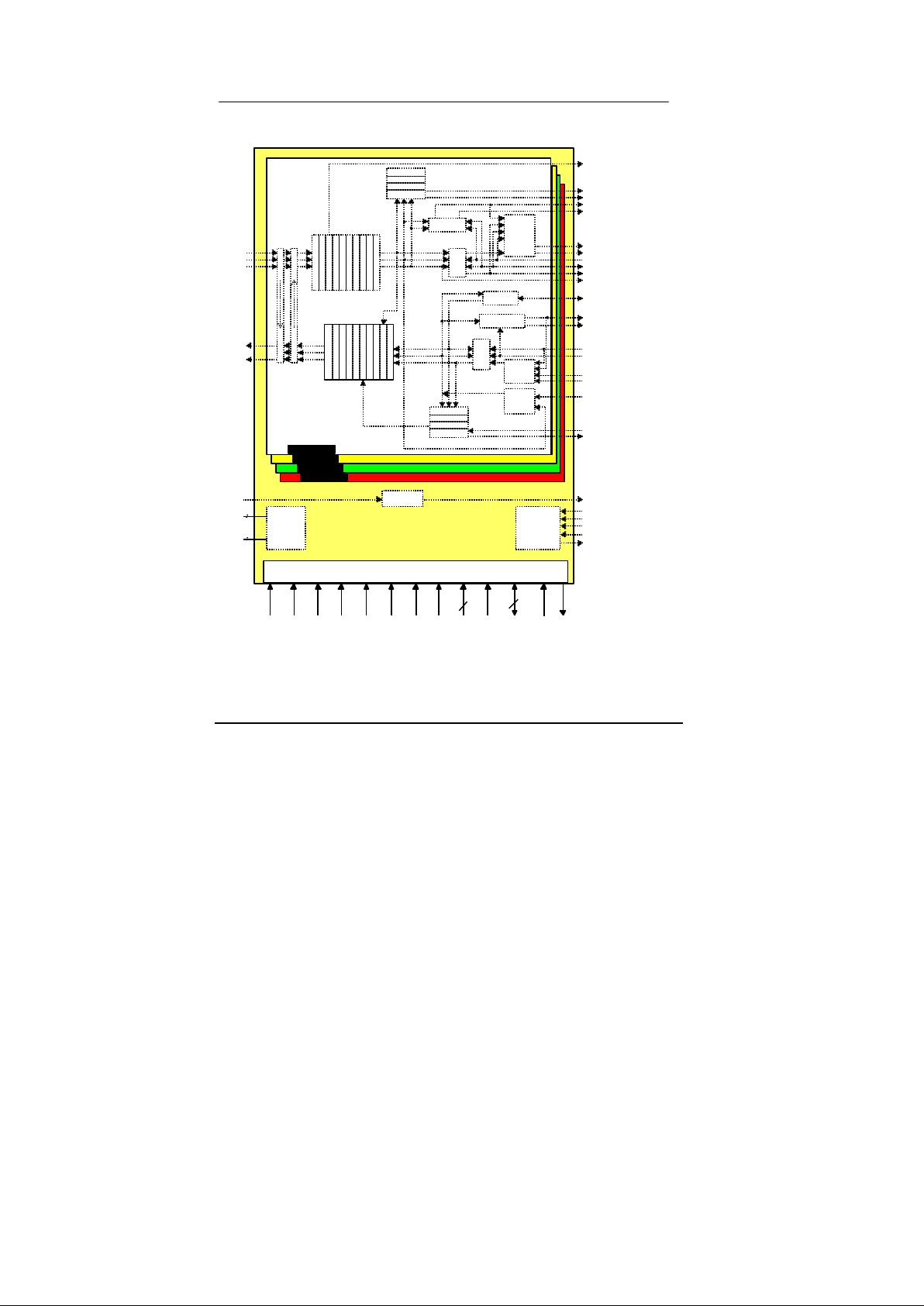
The DS21Q44 E1 is an enhanced version of the DS21Q43 Quad E1 Framer. The DS21Q44
contains four framers that are configured and read through a common microprocessor
compatible parallel port. Each framer consists of a receive framer, receive elastic store,
transmit formatter and transmit elastic store. All four framers in the DS21Q44 are totally
independent, they do not share a common framing synchronizer. Also the transmit and
receive sides of each framer are totally independent. The dual two-frame elastic stores
contained in each of the four framers can be independently enabled and disabled as required.
The device fully meets all of the latest E1 specifications including CCITT/ITU G.704,
G.706, G.962, and I.431 as well as ETS 300 011 and ETS 300 233.
6. DS21Q44 INTRODUCTION
The DS21Q44 is a superset version of the popular DS21Q43 Quad E1 framer offering the
new features listed below. All of the original features of the DS21Q43 have been retained and
software created for the original device is transferable to the DS21Q44. Setting the Framer
Mode Select (FMS) pin to a logic 1 allows the DS21Q44 to be used as a replacement for the
DS21Q43 allowing an existing design to use most of the new features. FMS is tied to
ground for the DS21FF44/DS21FT44.
New Features
• Aditional hardware signaling capability including:
– receive signaling reinsertion to a backplane multiframe sync
– availability of signaling in a separate PCM data stream
– signaling freezing
– interrupt generated on change of signaling data
• per–channel code insertion in both transmit and receive paths
• full HDLC controller with 64–byte buffers in both transmit and receive paths.
Configurable for Sa bits or DS0 access
• RCL, RLOS, RRA, and RUA1 alarms now interrupt on change of state
• 8.192 MHz clock synthesizer
• Ability to monitor one DS0 channel in both the transmit and receive paths
• Option to extend carrier loss criteria to a 1 ms period as per ETS 300 233
• Automatic RAI generation to ETS 300 011 specifications
• IEEE 1149.1 support
Functional Description

DALLAS SEMICONDUCTOR DS21FF44/DS21FT44
101899 16/119
The receive side in each framer locates FAS frame and CRC and CAS multiframe boundaries
as well as detects incoming alarms including, carrier loss, loss of synchronization, AIS and
Remote Alarm. If needed, the receive side elastic store can be enabled in order to absorb the
phase and frequency differences between the recovered E1 data stream and an asynchronous
backplane clock which is provided at the RSYSCLK input. The clock applied at the
RSYSCLK input can be either a 2.048 MHz clock or a 1.544 MHz clock. The RSYSCLK
can be a burst clock with speeds up to 8.192 MHz.
The transmit side in each framer is totally independent from the receive side in both the
clock requirements and characteristics. Data off of a backplane can be passed through a
transmit side elastic store if necessary. The transmit formatter will provide the necessary
frame/multiframe data overhead for E1 transmission.

DALLAS SEMICONDUCTOR DS21FF44/DS21FT44
101899 17/119
Reader’s Note: This data sheet assumes a particular nomenclature of the E1 operating
environment. In each 125 us frame, there are 32 eight–bit timeslots numbered 0 to 31.
Timeslot 0 is transmitted first and received first. These 32 timeslots are also referred to as
channels with a numbering scheme of 1 to 32. Timeslot 0 is identical to channel 1, timeslot
1 is identical to Channel 2, and so on. Each timeslot (or channel) is made up of eight bits
which are numbered 1 to 8. Bit number 1 is the MSB and is transmitted first. Bit number 8
is the LSB and is transmitted last. Throughout this data sheet, the following abbreviations
will be used:
FAS Frame Alignment Signal
CAS Channel Associated Signaling
MF Multiframe
Si International bits
CRC4 Cyclical Redundancy Check
CCS Common Channel Signaling
Sa Additional bits
E-bit CRC4 Error Bits
DALLAS SEMICONDUCTOR DS21FF44/DS21FT44
101899 18/119
DS21Q44 ENHANCED QUAD E1 FRAMER Figure 6-1
VSS
VDD
FRAMER #1
FRAMER #3
FRAMER #2
FRAMER #0
Parallel & Test Control Port
(routed to all blocks)
D0 to D7 /
AD0 to AD7
FS1
BTS
INT*
WR*
(R/W*)
RD*
(DS*)
FS0CS*TEST ALE
(AS)/
A6
A0 to A5,
A7
MUX
7
8
FMS
Framer Loopback
AIS Generation
HDB3 Encode
CRC4 Generation
FAS Word Insertion
Receive Side Framer
Transmit Side Formatter
BPV Counter
Alarm Detection
Per-Channel Code Insert
Elastic
Store
E-BIT Counter
sync
data
clock
sync
data
clock
TSYNC
TCLK
TCHCLK
TSER
TCHBLK
RCHCLK
RCHBLK
RLCLK
RMSYNC
TSSYNC
TSYSCLK
RLINK
RSER
RSYSCLK
RSYNC
RFSYNC
TLINK
TLCLK
Sa Extraction
Timing Control
Elastic
Store
Sync Control
Timing Control
HDB3 Decoder
Synchronizer
CRC Error Counter
FAS Error Counter
Signaling Extraction
SA and SI Extraction
Signaling
Buffer
RSIG
Hardware
Signaling
Insertion
TSIG
Remote Loopback
8MCLK
Per-Channel Code Insert
Per-Channel Loopback
64-Byte Buffer
RPOS
RCLK
RNEG
TPOS
TNEG
CLKS I
HDLC Engine
DS0 Insertion
Power
3
3
JTAG Port
JTRST*
JTMS
JTCLK
JTDI
JTDO
RLOS/LOTC
1
1
1
1
Note:
1. Alternate pin functions. Consult data sheet for restrictions.
LOTC DET
&
MUX
8.192MHz Clock
Synthesizer
Sa Insertion
64-Byte Buffer
HDLC Engine
DS0 Insertion
SI Bit Insertion
E-Bit Insertion
SA Insertion
Signaling Insertion

DALLAS SEMICONDUCTOR DS21FF44/DS21FT44
101899 19/119
7. DS21Q44 PIN FUNCTION DESCRIPTION
This section describes the signals on the DS21Q44 die. Signals which are not bonded out
or have limited functionality in the DS21FT44 and DS21FF44 are noted in italics.
TRANSMIT SIDE PINS
Signal Name: TCLK
Signal Description: Transmit Clock
Signal Type: Input
A 2.048 MHz primary clock. Used to clock data through the transmit side formatter.
Signal Name: TSER
Signal Description: Transmit Serial Data
Signal Type: Input
Transmit NRZ serial data. Sampled on the falling edge of TCLK when the transmit side
elastic store is disabled. Sampled on the falling edge of TSYSCLK when the transmit side
elastic store is enabled.
Signal Name: TCHCLK
Signal Description: Transmit Channel Clock
Signal Type: Output
A 256 KHz clock which pulses high during the LSB of each channel. Synchronous with
TCLK when the transmit side elastic store is disabled. Synchronous with TSYSCLK when
the transmit side elastic store is enabled. Useful for parallel to serial conversion of channel
data. This function is available when FMS = 1 (DS21Q43 emulation). This signal is not
bonded out in the DS21FF44/DS21FT44.
Signal Name: TCHBLK
Signal Description: Transmit Channel Block
Signal Type: Output
A user programmable output that can be forced high or low during any of the 32 E1
channels. Synchronous with TCLK when the transmit side elastic store is disabled.
Synchronous with TSYSCLK when the transmit side elastic store is enabled. Useful for
blocking clocks to a serial UART or LAPD controller in applications where not all E1
channels are used such as Fractional E1, 384 Kbps (H0), 768 Kbps, 1920 bps (H12) or
ISDN–PRI . Also useful for locating individual channels in drop–and–insert applications, for
external per–channel loopback, and for per–channel conditioning. See Section 16 for details.
This signal is not bonded out in the DS21FF44/DS21FT44.
Signal Name: TSYSCLK

DALLAS SEMICONDUCTOR DS21FF44/DS21FT44
101899 20/119
Signal Description: Transmit System Clock
Signal Type: Input
1.544 MHz or 2.048 MHz clock. Only used when the transmit side elastic store function is
enabled. Should be tied low in applications that do not use the transmit side elastic store.
Can be burst at rates up to 8.192 MHz. This pin is tied to the RSYSCLK signal in the
DS21FF44/DS21FT44.
Signal Name: TLCLK
Signal Description: Transmit Link Clock
Signal Type: Output
4 KHz to 20 KHz demand clock for the TLINK input. See Section 18 for details. This
signal is not bonded out in the DS21FF44/DS21FT44.
Signal Name: TLINK
Signal Description: Transmit Link Data
Signal Type: Input
If enabled, this pin will be sampled on the falling edge of TCLK for data insertion into any
combination of the Sa bit positions (Sa4 to Sa8). See Section 18 for details. This signal is
not bonded out in the DS21FF44/DS21FT44.
Signal Name: TSYNC
Signal Description: Transmit Sync
Signal Type: Input /Output
A pulse at this pin will establish either frame or multiframe boundaries for the transmit side.
This pin can also be programmed to output either a frame or multiframe pulse. Always
synchronous with TCLK.
Signal Name: TSSYNC
Signal Description: Transmit System Sync
Signal Type: Input
Only used when the transmit side elastic store is enabled. A pulse at this pin will establish
either frame or multiframe boundaries for the transmit side. Should be tied low in
applications that do not use the transmit side elastic store. Always synchronous with
TSYSCLK.
Signal Name: TSIG
Signal Description: Transmit Signaling Input
Signal Type: Input
When enabled, this input will sample signaling bits for insertion into outgoing PCM E1
data stream. Sampled on the falling edge of TCLK when the transmit side elastic store is

DALLAS SEMICONDUCTOR DS21FF44/DS21FT44
101899 21/119
disabled. Sampled on the falling edge of TSYSCLK when the transmit side elastic store is
enabled. This function is available when FMS = 0. FMS is tied to ground for the
DS21FF44/DS21FT44.
Signal Name: TPOS
Signal Description: Transmit Positive Data Output
Signal Type: Output
Updated on the rising edge of TCLK with the bipolar data out of the transmit side formatter.
Can be programmed to source NRZ data via the Output Data Format (TCR1.7) control bit.
Signal Name: TNEG
Signal Description: Transmit Negative Data Output
Signal Type: Output
Updated on the rising edge of TCLK with the bipolar data out of the transmit side formatter.
RECEIVE SIDE PINS
Signal Name: RLINK
Signal Description: Receive Link Data
Signal Type: Output
Updated with full recovered E1 data stream on the rising edge of RCLK. This signal is not
bonded out in the DS21FF44/DS21FT44.
Signal Name: RLCLK
Signal Description: Receive Link Clock
Signal Type: Output
A 4 KHz to 20 KHz clock for the RLINK output. Used for sampling Sa bits. This signal is
not bonded out in the DS21FF44/DS21FT44.
Signal Name: RCLK
Signal Description: Receive Clock Input
Signal Type: Input
2.048 MHz clock that is used to clock data through the receive side framer.
Signal Name: RCHCLK
Signal Description: Receive Channel Clock
Signal Type: Output
A 256 KHz clock which pulses high during the LSB of each channel. Synchronous with
RCLK when the receive side elastic store is disabled. Synchronous with RSYSCLK when
the receive side elastic store is enabled. Useful for parallel to serial conversion of channel

DALLAS SEMICONDUCTOR DS21FF44/DS21FT44
101899 22/119
data. This function is available when FMS = 1 (DS21Q43 emulation). This signal is not
bonded out in the DS21FF44/DS21FT44.
Signal Name: RCHBLK
Signal Description: Receive Channel Block
Signal Type: Output
A user programmable output that can be forced high or low during any of the 32 E1
channels. Synchronous with RCLK when the receive side elastic store is disabled.
Synchronous with RSYSCLK when the receive side elastic store is enabled. Useful for
blocking clocks to a serial UART or LAPD controller in applications where not all E1
channels are used such as Fractional E1, 384K bps service, 768K bps, or ISDN–PRI. Also
useful for locating individual channels in drop–and–insert applications, for external per–
channel loopback, and for per–channel conditioning. See Section 16 for details.
Signal Name: RSER
Signal Description: Receive Serial Data
Signal Type: Output
Received NRZ serial data. Updated on rising edges of RCLK when the receive side elastic
store is disabled. Updated on the rising edges of RSYSCLK when the receive side elastic
store is enabled.
Signal Name: RSYNC
Signal Description: Receive Sync
Signal Type: Input /Output
An extracted pulse, one RCLK wide, is output at this pin which identifies either frame or
CAS/CRC multiframe boundaries. If the receive side elastic store is enabled, then this pin
can be enabled to be an input at which a frame or multiframe boundary pulse synchronous
with RSYSCLK is applied.
Signal Name: RFSYNC
Signal Description: Receive Frame Sync
Signal Type: Output
An extracted 8 KHz pulse, one RCLK wide, is output at this pin which identifies frame
boundaries. This signal is not bonded out in the DS21FF44/DS21FT44.
Signal Name: RMSYNC
Signal Description: Receive Multiframe Sync
Signal Type: Output
An extracted pulse, one RSYSCLK wide, is output at this pin which identifies multiframe
boundaries. If the receive side elastic store is disabled, then this output will output

DALLAS SEMICONDUCTOR DS21FF44/DS21FT44
101899 23/119
multiframe boundaries associated with RCLK. This function is available when FMS = 1
(DS21Q43 emulation). This signal is not bonded out in the DS21FF44/DS21FT44.
Signal Name: RSYSCLK
Signal Description: Receive System Clock
Signal Type: Input
1.544 MHz or 2.048 MHz clock. Only used when the elastic store function is enabled.
Should be tied low in applications that do not use the elastic store. Can be burst at rates up
to 8.192 MHz. This pin is tied to the TSYSCLK signal in the DS21FF44/DS21FT44.
Signal Name: RSIG
Signal Description: Receive Signaling Output
Signal Type: Output
Outputs signaling bits in a PCM format. Updated on rising edges of RCLK when the
receive side elastic store is disabled. Updated on the rising edges of RSYSCLK when the
receive side elastic store is enabled. This function is available when FMS = 0. FMS is tied
to ground for the DS21FF44/DS21FT44.
Signal Name: RLOS/LOTC
Signal Description: Receive Loss of Sync / Loss of Transmit Clock
Signal Type: Output
A dual function output that is controlled by the TCR2.0 control bit. This pin can be
programmed to either toggle high when the synchronizer is searching for the frame and
multiframe or to toggle high if the TCLK pin has not been toggled for 5 usec. This function
is available when FMS = 1 (DS21Q43 emulation). This signal is not bonded out in the
DS21FF44/DS21FT44.
Signal Name: CLKSI
Signal Description: 8 MHz Clock Reference
Signal Type: Input
A 2.048 MHz reference clock used in the generation of 8MCLK. This function is available
when FMS = 0. FMS is tied to ground for the DS21FF44/DS21FT44.
Signal Name: 8MCLK
Signal Description: 8 MHz Clock
Signal Type: Output
A 8.192 MHz output clock that is referenced to the clock that is input at the CLKSI pin.
This function is available when FMS = 0. FMS is tied to ground for the
DS21FF44/DS21FT44.
Signal Name: RPOS

DALLAS SEMICONDUCTOR DS21FF44/DS21FT44
101899 24/119
Signal Description: Receive Positive Data Input
Signal Type: Input
Sampled on the falling edge of RCLK for data to be clocked through the receive side framer.
RPOS and RNEG can be tied together for an NRZ interface. Connecting RPOS to RNEG
disables the bipolar violation monitoring circuitry.
Signal Name: RNEG
Signal Description: Receive Negative Data Input
Signal Type: Input
Sampled on the falling edge of RCLK for data to be clocked through the receive side framer.
RPOS and RNEG can be tied together for an NRZ interface. Connecting RPOS to RNEG
disables the bipolar violation monitoring circuitry.
PARALLEL CONTROL PORT PINS
Signal Name: INT*
Signal Description: Interrupt
Signal Type: Output
Flags host controller during conditions and change of conditions defined in the Status
Registers 1 and 2 and the FDL Status Register. Active low, open drain output.
Signal Name: FMS
Signal Description: Framer Mode Select
Signal Type: Input
Set low to select DS21Q44 feature set. Set high to select DS21Q43 emulation. FMS is tied
to ground for the DS21FF44/DS21FT44.
Signal Name: MUX
Signal Description: Bus Operation
Signal Type: Input
Set low to select non–multiplexed bus operation. Set high to select multiplexed bus
operation.
Signal Name: D0 TO D7 / AD0 TO AD7
Signal Description: Data Bus or Address/Data Bus
Signal Type: Input /Output
In non–multiplexed bus operation (MUX = 0), serves as the data bus. In multiplexed bus
operation (MUX = 1), serves as a 8–bit multiplexed address / data bus.
Signal Name: A0 TO A5, A7
Signal Description: Address Bus
Signal Type: Input

DALLAS SEMICONDUCTOR DS21FF44/DS21FT44
101899 25/119
In non–multiplexed bus operation (MUX = 0), serves as the address bus. In multiplexed bus
operation (MUX = 1), these pins are not used and should be tied low.
Signal Name: ALE (AS) / A6
Signal Description: Address Latch Enable (Address Strobe) or A6
Signal Type: Input
In non–multiplexed bus operation (MUX = 0), serves as address bit 6. In multiplexed bus
operation (MUX = 1), serves to demultiplex the bus on a positive–going edge.
Signal Name: BTS
Signal Description: Bus Type Select
Signal Type: Input
Strap high to select Motorola bus timing; strap low to select Intel bus timing. This pin
controls the function of the RD*(DS*), ALE(AS), and WR*(R/W*) pins. If BTS = 1, then
these pins assume the function listed in parenthesis ().
Signal Name: RD* (DS*)
Signal Description: Read Input (Data Strobe)
Signal Type: Input
RD* and DS* are active low signals. Note: DS is active high when MUX=1. Refer to bus
timing diagrams in section 23 .
Signal Name: FS0 AND FS1
Signal Description: Framer Selects
Signal Type: Input
Selects which of the four framers to be accessed.
Signal Name: CS*
Signal Description: Chip Select
Signal Type: Input
Must be low to read or write to the device. CS* is an active low signal.
Signal Name: WR* (R/W*)
Signal Description: Write Input (Read/Write)
Signal Type: Input
WR* is an active low signal.
TEST ACCESS PORT PINS
Signal Name: TEST
Signal Description: 3–State Control
Signal Type: Input

DALLAS SEMICONDUCTOR DS21FF44/DS21FT44
101899 26/119
Set high to 3–state all output and I/O pins (including the parallel control port). Set low for
normal operation. Useful in board level testing.
Signal Name: JTRST*
Signal Description: IEEE 1149.1 Test Reset
Signal Type: Input
This signal is used to asynchronously reset the test access port controller. At power up,
JTRST* must be set low and then high. This action will set the device into the boundary
scan bypass mode allowing normal device operation. If boundary scan is not used, this pin
should be held low. This function is available when FMS = 0. FMS is tied to ground for
the DS21FF44/DS21FT44.
Signal Name: JTMS
Signal Description: IEEE 1149.1 Test Mode Select
Signal Type: Input
This pin is sampled on the rising edge of JTCLK and is used to place the test port into the
various defined IEEE 1149.1 states. If not used, this pin should be pulled high. This
function is available when FMS = 0. FMS is tied to ground for the DS21FF44/DS21FT44.
Signal Name: JTCLK
Signal Description: IEEE 1149.1 Test Clock Signal
Signal Type: Input
This signal is used to shift data into JTDI on the rising edge and out of JTDO on the falling
edge. If not used, this pin should be tied to VSS. This function is available when FMS = 0.
Signal Name: JTDI
Signal Description: IEEE 1149.1 Test Data Input
Signal Type: Input
Test instructions and data are clocked into this pin on the rising edge of JTCLK. If not
used, this pin should be pulled high. This function is available when FMS = 0. FMS is
tied to ground for the DS21FF44/DS21FT44.
Signal Name: JTDO
Signal Description: IEEE 1149.1 Test Data Output
Signal Type: Output
Test instructions and data are clocked out of this pin on the falling edge of JTCLK. If not
used, this pin should be left unconnected. This function is available when FMS = 0. FMS
is tied to ground for the DS21FF44/DS21FT44.

DALLAS SEMICONDUCTOR DS21FF44/DS21FT44
101899 27/119
SUPPLY PINS
Signal Name: VDD
Signal Description: Positive Supply
Signal Type: Supply
2.97 to 3.63 volts.
Signal Name: VSS
Signal Description: Signal Ground
Signal Type: Supply
0.0 volts.
DALLAS SEMICONDUCTOR DS21FF44/DS21FT44
101899 28/119
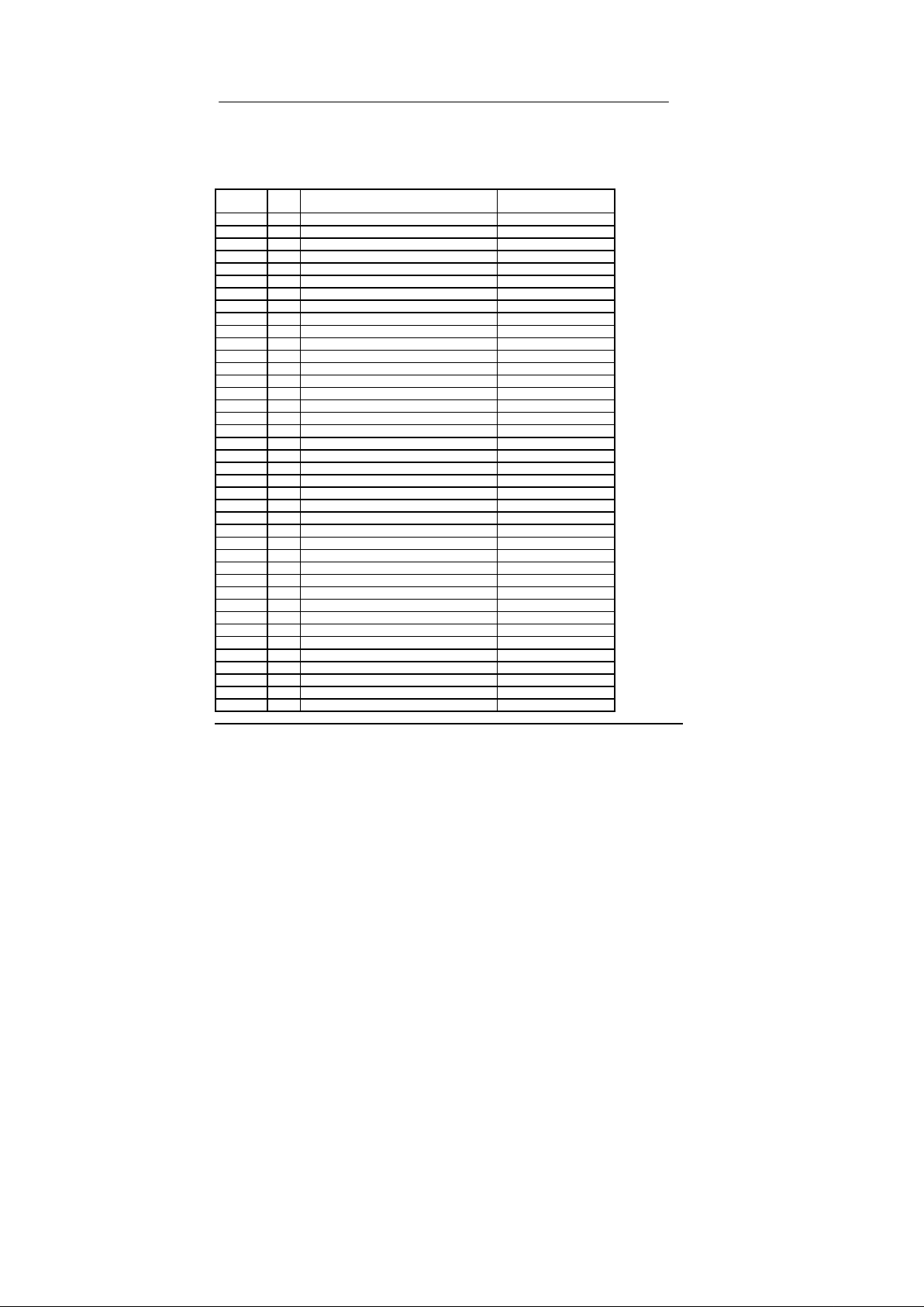
8. DS21Q44 REGISTER MAP
Register Map Sorted by Address Table 8-1
ADDRESS R/W REGISTER NAME REGISTER
ABBREVIATION
00 R BPV or Code Violation Count 1 VCR1
01 R BPV or Code Violation Count 2 VCR2
02 R CRC4 Error Count 1 / FAS Error Count 1 CRCCR1
03 R CRC4 Error Count 2 CRCCR2
04 R E-Bit Count 1 / FAS Error Count 2 EBCR1
05 R E-Bit Count 2 EBCR2
06 R/W Status 1 SR1
07 R/W Status 2 SR2
08 R/W Receive Information RIR
09 R/W Test 2 TEST2 (set to 00h)
0A – Not used (set to 00H)
0B – Not used (set to 00H)
0C – Not used (set to 00H)
0D – Not used (set to 00H)
0E – Not used (set to 00H)
0F R Device ID IDR
10 R/W Receive Control 1 RCR1
11 R/W Receive Control 2 RCR2
12 R/W Transmit Control 1 TCR1
13 R/W Transmit Control 2 TCR2
14 R/W Common Control 1 CCR1
15 R/W Test 1 TEST1 (set to 00h)
16 R/W Interrupt Mask 1 IMR1
17 R/W Interrupt Mask 2 IMR2
18 – Not used (set to 00H)
19 – Not used (set to 00H)
1A R/W Common Control 2 CCR2
1B R/W Common Control 3 CCR3
1C R/W Transmit Sa Bit Control TSaCR
1D R/W Common Control 6 CCR6
1E R Synchronizer Status SSR
1F R Receive Non-Align Frame RNAF
20 R/W Transmit Align Frame TAF
21 R/W Transmit Non-Align Frame TNAF
22 R/W Transmit Channel Blocking 1 TCBR1
23 R/W Transmit Channel Blocking 2 TCBR2
24 R/W Transmit Channel Blocking 3 TCBR3
25 R/W Transmit Channel Blocking 4 TCBR4
26 R/W Transmit Idle 1 TIR1
27 R/W Transmit Idle 2 TIR2
DALLAS SEMICONDUCTOR DS21FF44/DS21FT44
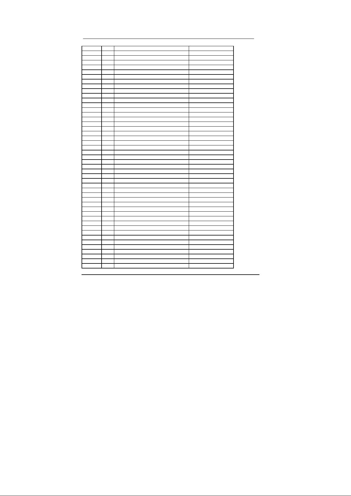
101899 29/119
28 R/W Transmit Idle 3 TIR3
29 R/W Transmit Idle 4 TIR4
2A R/W Transmit Idle Definition TIDR
2B R/W Receive Channel Blocking 1 RCBR1
2C R/W Receive Channel Blocking 2 RCBR2
2D R/W Receive Channel Blocking 3 RCBR3
2E R/W Receive Channel Blocking 4 RCBR4
2F R Receive Align Frame RAF
30 R Receive Signaling 1 RS1
31 R Receive Signaling 2 RS2
32 R Receive Signaling 3 RS3
33 R Receive Signaling 4 RS4
34 R Receive Signaling 5 RS5
35 R Receive Signaling 6 RS6
36 R Receive Signaling 7 RS7
37 R Receive Signaling 8 RS8
38 R Receive Signaling 9 RS9
39 R Receive Signaling 10 RS10
3A R Receive Signaling 11 RS11
3B R Receive Signaling 12 RS12
3C R Receive Signaling 13 RS13
3D R Receive Signaling 14 RS14
3E R Receive Signaling 15 RS15
3F R Receive Signaling 16 RS16
40 R/W Transmit Signaling 1 TS1
41 R/W Transmit Signaling 2 TS2
42 R/W Transmit Signaling 3 TS3
43 R/W Transmit Signaling 4 TS4
44 R/W Transmit Signaling 5 TS5
45 R/W Transmit Signaling 6 TS6
46 R/W Transmit Signaling 7 TS7
47 R/W Transmit Signaling 8 TS8
48 R/W Transmit Signaling 9 TS9
49 R/W Transmit Signaling 10 TS10
4A R/W Transmit Signaling 11 TS11
4B R/W Transmit Signaling 12 TS12
4C R/W Transmit Signaling 13 TS13
4D R/W Transmit Signaling 14 TS14
4E R/W Transmit Signaling 15 TS15
4F R/W Transmit Signaling 16 TS16
50 R/W Transmit Si Bits Align Frame TSiAF
51 R/W Transmit Si Bits Non-Align Frame TSiNAF
52 R/W Transmit Remote Alarm Bits TRA
53 R/W Transmit Sa4 Bits TSa4
54 R/W Transmit Sa5 Bits TSa5
55 R/W Transmit Sa6 Bits TSa6
56 R/W Transmit Sa7 Bits TSa7

DALLAS SEMICONDUCTOR DS21FF44/DS21FT44
101899 30/119
57 R/W Transmit Sa8 Bits TSa8
58 R Receive Si bits Align Frame RSiAF
59 R Receive Si bits Non-Align Frame RSiNAF
5A R Receive Remote Alarm Bits RRA
5B R Receive Sa4 Bits RSa4
5C R Receive Sa5 Bits RSa5
5D R Receive Sa6 Bits RSa6
5E R Receive Sa7 Bits RSa7
5F R Receive Sa8 Bits RSa8
60 R/W Transmit Channel 1 TC1
61 R/W Transmit Channel 2 TC2
62 R/W Transmit Channel 3 TC3
63 R/W Transmit Channel 4 TC4
64 R/W Transmit Channel 5 TC5
65 R/W Transmit Channel 6 TC6
66 R/W Transmit Channel 7 TC7
67 R/W Transmit Channel 8 TC8
68 R/W Transmit Channel 9 TC9
69 R/W Transmit Channel 10 TC10
6A R/W Transmit Channel 11 TC11
6B R/W Transmit Channel 12 TC12
6C R/W Transmit Channel 13 TC13
6D R/W Transmit Channel 14 TC14
6E R/W Transmit Channel 15 TC15
6F R/W Transmit Channel 16 TC16
70 R/W Transmit Channel 17 TC17
71 R/W Transmit Channel 18 TC18
72 R/W Transmit Channel 19 TC19
73 R/W Transmit Channel 20 TC20
74 R/W Transmit Channel 21 TC21
75 R/W Transmit Channel 22 TC22
76 R/W Transmit Channel 23 TC23
77 R/W Transmit Channel 24 TC24
78 R/W Transmit Channel 25 TC25
79 R/W Transmit Channel 26 TC26
7A R/W Transmit Channel 27 TC27
7B R/W Transmit Channel 28 TC28
7C R/W Transmit Channel 29 TC29
7D R/W Transmit Channel 30 TC30
7E R/W Transmit Channel 31 TC31
7F R/W Transmit Channel 32 TC32
80 R/W Receive Channel 1 RC1
81 R/W Receive Channel 2 RC2
82 R/W Receive Channel 3 RC3
83 R/W Receive Channel 4 RC4
84 R/W Receive Channel 5 RC5
85 R/W Receive Channel 6 RC6
 Loading...