Dallas Semiconductor DS2187, DS2187S Datasheet

1 of 10 112099
FEATURES
Line interface for T1 (1.544 MHz) and CEPT
(2.048 MHz) primary rate networks
Extracts clock and data from twisted pair or
coax
Meets requirements of PUB 43801, TR
62411, and applicable CCITT G.823
Precision on-chip PLL eliminates external
crystal or LC tank - no tuning required
Decodes AMI, B8ZS, and HDB3 coded
signals
Designed for short loop applications such as
terminal equipment to DSX-1
Reports alarm and error events
Compatible with the DS2180A T1/ISDN
Primary Rate and DS2181A CEPT
Transceivers, as well as DS2141A T1 and
DS2143 E1 Controllers
Companion to the DS2186 T1/CEPT
Transmit Line Interface and DS2188
T1/CEPT Jitter Attenuator
Single 5V supply; low-power CMOS
technology
PIN ASSIGNMENT
DESCRIPTION
The DS2187 T1/CEPT Receive Line Interface chip interfaces user equipment to North American (T1
1.544 MHz) and European (CEPT 2.048 MHz) primary rate communication networks. The device
extracts clock and data from twisted pair or coax transmission media and eliminates expensive discrete
components and/or manual tuning required in existing T1 and CEPT line termination electronics.
Application areas include DACS, CSU, CPE, channel banks, and PABX-to-computer interfaces such as
DMI and CPI.
DS2187
Receive Line Interface
www.dalsemi.com
AVDD 1 20 DVDD
RAIS 2 19 RCL
ZCSEN 3 18 AIS
NC 4 17 BPV
LCAP 5 16 NC
RCLKSEL 6 15 NC
RTIP 7 14 RPOS
RRING 8 13 RNEG
LOCK 9 12 RCLK
AVSS 10 11 DVSS
20-Pin SOIC (300-mil)
AVDD 1 18 DVDD
RAIS 2 17 RCL
ZCSEN 3 16 AIS
LCAP 4 15 BPV
RCLKSEL 5 14 NC
RTIP 6 13 RPOS
RRING 7 12 RNEG
LOCK 8 11 RCLK
AVSS 9 10 DVSS
18-Pin DIP (300-mil)

DS2187
2 of 10
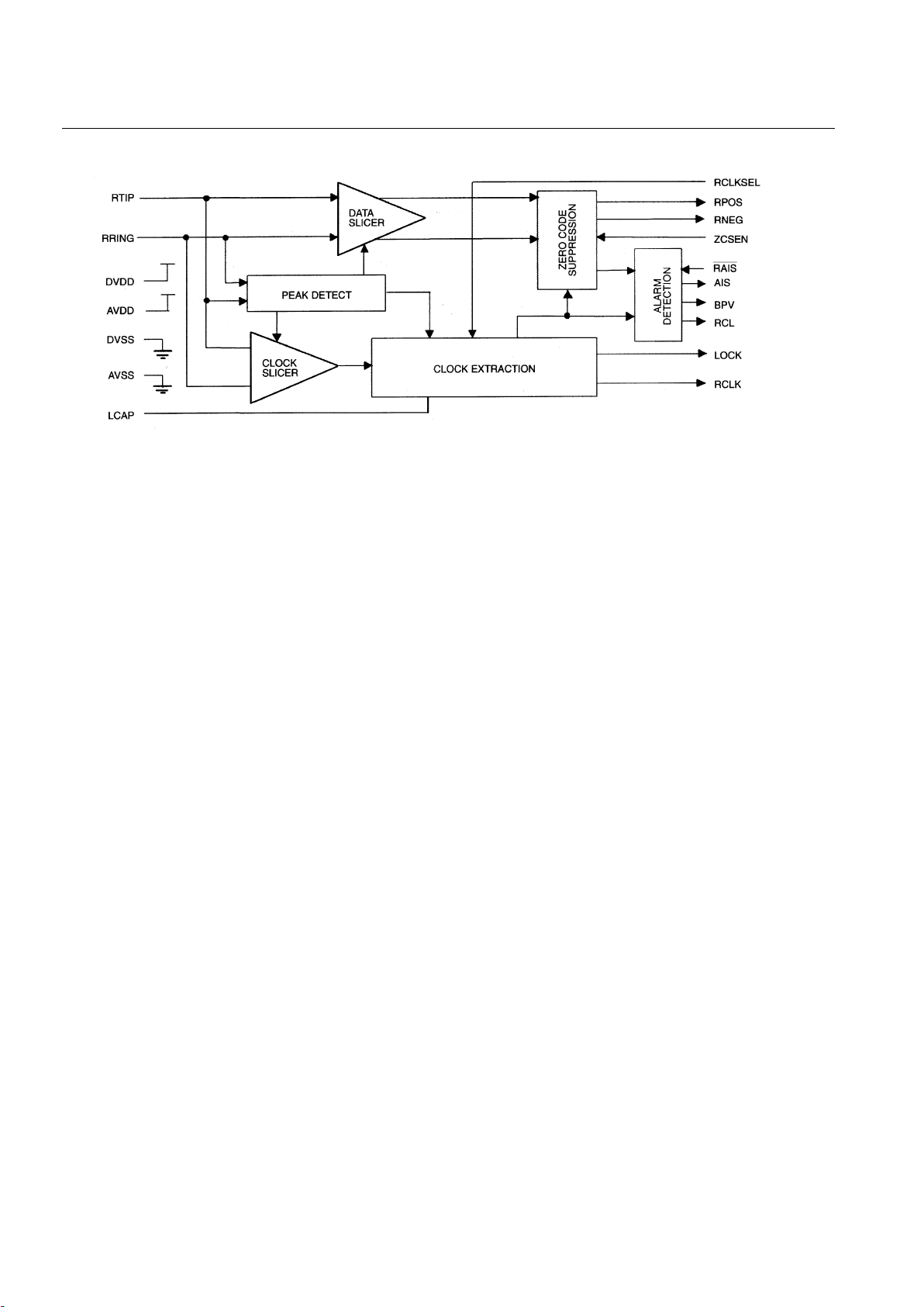
DS2187 BLOCK DIAGRAM Figure 1
LINE INPUT
Input signals are coupled to the DS2187 via a 1:2 center-tapped transformer as shown in Figure 2. For T1
applications, R1 and R2 must be 200 ohms in order to properly terminate the line at 100 ohms. R1 and R2
are set at 150 or 240 ohms for CEPT applications. Special internal circuitry of the RTIP and RRING
inputs permits negative signal excursions below VSS, which will occur in the circuit in Figure 2.
PEAK DETECTOR AND SLICERS
Signal pulses present at RTIP and RR ING are sampled by an internal peak detect circuit. The clock and
data slicer threshold are set for 50% of the sampled peak voltage.
Peak input levels at RRIP and RRING must exceed 0.6 volts to establish minimum slicer thresholds.
Signals below this level will cause RCL to transition high after 192 bit times.
CLOCK EXTRACTION
The DS2187 utilizes both frequency locked (FLL) and digital phase locked (DPLL) loops to recover data
and clock from the incoming AMI signal. T1 applications utilize a 18.528 MHz clock divided by either
11, 12, or 13 to match the phase of the incoming jittered line signal. This technique affords exceptional
jitter tracking which enables the DS2187 to meet the latest AT&T TR 62411 and ECSA jitter
specifications. A 24.576 MHz clock divided by 11, 12, or 13 provides jitter tra cking in the CEPT mode.
The DPLL output is buffered and presented at RCLK. An on-chip, laser-trimmed, voltage-controlled
oscillator (V
CO
) provides the precision 18.528 MHz and 24.576 MHz frequency sources utilized in the
FLL. The FLL is a high-Q circuit which tracks the average frequency of the incoming signal, minimizing
the effect of the DPLL on output jitter.
During the acquisition time or if RCL goes high, the LOCK pin will go low to indicate a loss of
synchronization to the line signal. Once this pin goes high, the FLL has achieved frequency lock and
valid data is present at the RPOS and RNEG outputs.

DS2187
3 of 10
PIN DESCRIPTION Table 1
PIN SYMBOL TYPE DESCRIPTION
1AVDD -Analog Positive Supply. 5.0 volts.
2
RAIS
I
Reset Alarm Indication Signal. Every other low pulse at this input
establishes the AIS alarm detection period.
3 ZCSEN I
0 Code Suppression Enable. When high, incoming B8ZS (RCLKSEL=0)
or HDB3 (RCLKSEL=1) code words are replaced with all 0s at RPOS and
RNEG; when low, no code replacement occurs.
4LCAP -Loop Cap. Part of internal loop filter; attach a 10 microfarad capacitor from
this pin to V
SS
.
5 RCLKSEL I
Receive Clock Select. Tie to V
SS
for 1.544 MHz (T1) applications, to VDD for
2.048 MHz (CEPT) applications.
6
7
RTIP
RRING
I Receive Tip and Ring. Connect to line transformer as shown in Figure 2.
8 LOCK OFrequency Lock. High state indicates that internal circuitry is phase- and
frequency-locked to the incoming signal at RRING and RTIP.
9 AVSS -Analog Signal Ground. 0.0 volts.
10 DVSS - Digital Signal Ground. 0.0 volts.
11 RCLK O Receive Clock. Extracted line rate clock.
12
13
RNEG
RPOS
O Receive Data. Extracted receive data; updated on rising edge of RCLK.
14 NC - No Connect. Do not connect to this pin.
15 BPV O Bipolar Violation. Transitions high for the full bit period when a bit in
violation appears at RPOS or RNEG; B8ZS code words are not accused when
ZCSEN=1. BPV not valid for RCLKSEL=1 and ZCSEN=1.
16 AIS O
Alarm Indication Signal. High when the received data stream has contained
less than three 0s during the last two periods of the
RAIS signal.
17 RCL O Receive Carrier Loss. High if 192 0s appear at RPOS and RNEG; reset on
next occurrence of a one.
18 DVDD - Digital Positive Supply. 5.0 volts
 Loading...