1 of 15 091599
FEATURES
§ Synchronizes loop–timed and system–timed
T1 data streams
§ Two–frame buffer depth; slips occur on frame
boundaries
§ Output indicates when slip occurs
§ Buffer may be recentered externally
§ Ideal for 1.544 to 2.048 MHz rate conversion
§ Interfaces to parallel or serial backplanes
§ Extracts and buffers robbed–bit signaling
§ Inhibits signaling updates during alarm or slip
conditions
§ Integration feature “debounces” signaling
§ Slip–compensated output indicates when
signaling updates occur
§ Compatible with DS2180A T1 Transceiver
§ Surface mount package available, designated
DS2176Q
§ Industrial temperature range of –40°C to
+85°C available, designated DS2176N
PIN ASSIGNMENT
DESCRIPTION
The DS2176 is a low–power CMOS device specifically designed for synchronizing receive side loop–
timed T–carrier data streams with system side timing. The device has several flexible operating modes
which simplify interfacing incoming data to parallel and serial TDM backplanes. The device extracts,
buffers and integrates ABCD signaling; signaling updates are prohibited during alarm or slip conditions.
The buffer replaces extensive hardware in existing applications with one “skinny” 24–lead package.
Application areas include digital trunks, drop and insert equipment, transcoders, digital cross–connects
(DACS), private network equipment and PABX–to–computer interfaces such as DMI and CPI.
DS2176
T1 Receive Buffer
www.dalsemi.com
23
RCLK
ACD
SCHCLK
SM0
SM1
VSS
VDD
SYCLK
SSER
SLIP
SBIT8
SMSYNC
SIGFRZ
SFSYNC
ALN
FMS
S/P1234567891011122422
212019181716151413
RMSYN
RSER
B
SIGH
24-PIN 300 MIL DIP
28-PIN PLCC
A
B
NC
NC
C
D
SSER
SLIP
SBIT8
NC
NC
SMSYNC
SCHCLK
SIGFRZ
RSER
RCLK
RMSYNC
SIGH
VDD
SCKLSEL
SYSCLK
SM0
SM1
VSS
S/P
FMS
ALN
SFSYNC
25
24
23
22
21
20
19
5
6
7
8
9
10
11
4 3 2 1 28 27 26
12 13 14 15 16 17 18

DS2176
2 of 15
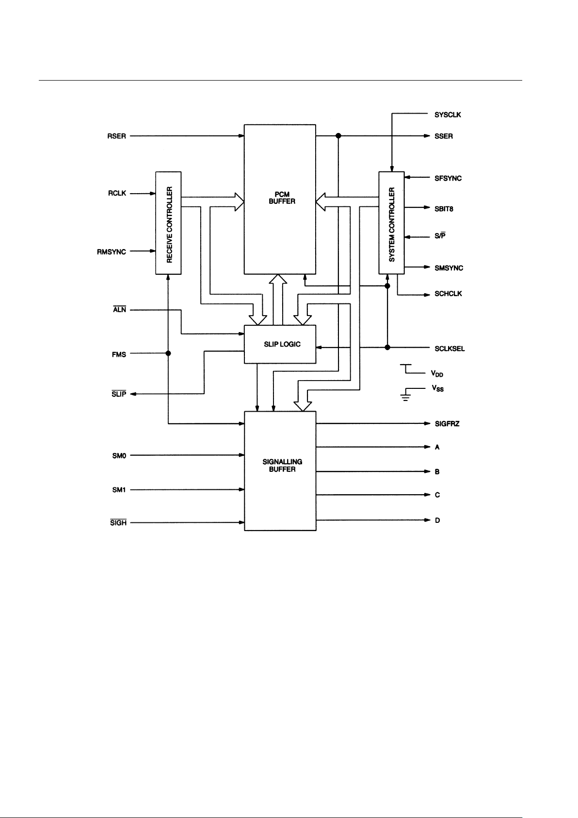
DS2176 BLOCK DIAGRAM Figure 1

DS2176
3 of 15
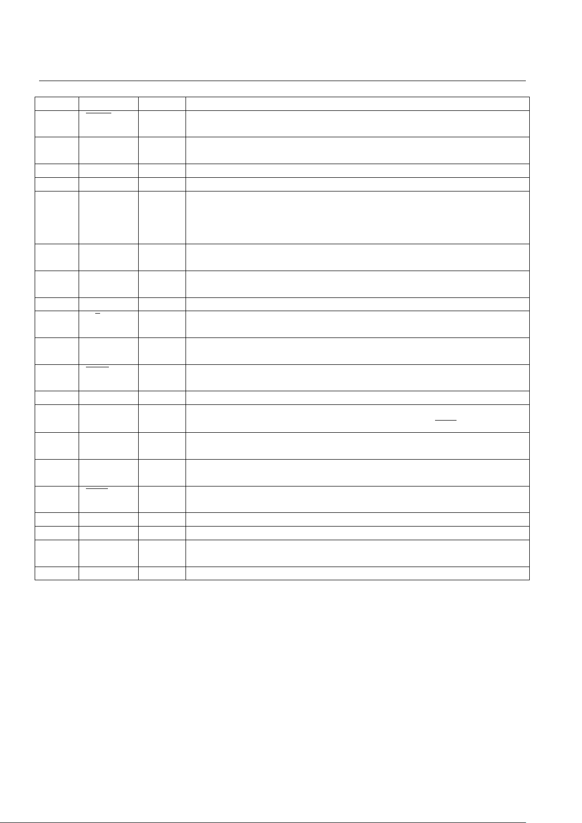
PIN DESCRIPTION Table 1
PIN SYMBOL TYPE DESCRIPTION
1
SIGN
I Signaling Inhibit. When low, ABCD signaling updates are disabled for
a period determined by SM0 and SM1, or until returned high.
2 RMSYNC I Receive Multifram Sync. Must be pulsed high at multiframe
boundaries to establish frame and multiframe alignment.
3 RCLK I Receive Clock. Primary 1.544 MHz clock.
4 RSER I Receive Serial Data. Sampled on Falling edge of RCLK.
5
6
7
8
A
B
C
D
O
Robbed-Bit Signaling Outputs.
9 SCHCLK O System Channel Clock. Transitions high on channel boundaries; useful
for serial to parallel conversion of channel data.
10
11
SM0
SM1
I Signaling Modes 0 and 1. Select signaling supervision technique.
12 V
SS
– Signal Ground. 0.0 volts.
13
S/
P
I Serial/Parallel Select. Tie to V
SS
for parallel backplane applications, to
VDD for serial.
14 FMS I Frame Mode Select. Tie to VSS to select 193S(D4) framing to VDD for
193E (extended).
15
ALN
I Align. Recenters buffer on next system side frame boundary when
forced low.
16 SFSYNC I System Frame Sync. Rising edge establishes start of frame.
17 SIGFRZ O Signaling Freeze. When high, indicates signaling updates have been
disabled internally via a slip or externally by forcing SIGH low.
18 SMSYNC O System Multiframe Sync. Slip-compensated multiframe output;
indicates when signaling updates are made.
19 SBIT8 O System Bit 8. High during the LSB time of each channel. Used to
reinsert extracted signaling into outgoing data stream.
20
SLIP
O Frame Slip. Active low, open collector output. Held low for 65
SYSCLK cycles when a slip occurs.
21 SSER O System Serial Out. Updated on rising edge of SYSCLK.
22 SYSCLK I System Clock. 1.544 or 2.048 MHz data clock.
23 SCLKSEL I System Clock Select. Tie to VSS for 1.544 MHz applications, to VDD for
2.048 MHz.
24 V
DD
– Positive Supply. 5.0 volts.

DS2176
4 of 15
OVERVIEW
The DS2176 performs two primary functions: 1) synchronization of received T1 PCM data (looped
timed) to host backplane frequencies; 2) supervision of robbed–bit signaling data embedded in the data
stream. The buffer, while optimized for use with the DS2180A T1 Transceiver, is also compatible with
other transceiver devices. The DS2180A data sheet should serve as a valuable reference when designing
with the DS2176.
RECEIVE SIDE TIMING FIGURE 2
DATA SYNCHRONIZATION
PCM BUFFER
The DS2176 utilizes a 2–frame buffer (386 bits) to synchronize incoming PCM data to the system
backplane clock. The buffer samples data at RSER on the falling edge of RCLK. Output data appears at
SSER and is up-dated on the rising edge of SYSCLK. A rising edge at RMSYNC establishes receive side
frame and multi-frame alignment. A rising edge at SFSYNC establishes system side frame alignment.
The buffer depth is constantly monitored by onboard contention logic; a “slip” occurs when the buffer is
completely emptied or filled. Slips automatically recenter the buffer to a one–frame depth and always
occur on frame boundaries.
SLIP CORRECTION CAPABILITY
The 2–frame buffer depth is adequate for most T–carrier applications where short–term jitter
synchronization, rather than correction of significant frequency differences, is required. The DS2176
provides an ideal balance between total delay and slip correction capability.
BUFFER RECENTERING
Many applications require that the buffer be recentered during system power–up and/or initialization.
Forcing ALN low recenters the buffer on the occurrence of the next frame sync boundary. A slip will
occur during this recentering if the buffer depth is adjusted. If the depth is presently optimum, no
adjustment (slip) occurs. SLIP is held low for 65 SYSCLK cycles when a slip occurs. SLIP is an active–
low, open collector output.
BUFFER DEPTH MONITORING
SMSYNC is a system side output pulse which indicates system side multiframe boundaries. The distance
between rising edges at RMSYNC and SMSYNC indicates the current buffer depth. Slip direction and/or
an impending slip condition may be determined by monitoring RMSYNC and SMSYNC real time.
SMSYNC is held high for 65 SYSCLK cycles.
CLOCK SELECT
The device is compatible with two common backplane frequencies: 1.544 MHz, selected when
SCLKSEL=0; and 2.048 MHz, selected when SCLKSEL=1. In 1.544 MHz applications the F–bit is

DS2176
5 of 15
passed through the receive buffer and presented at SSER immediately after the rising edge of the system
side frame sync. The F–bit is dropped in 2.048 MHz applications and the MSB of channel 1 appears at
SSER one bit period after a rising edge at SFSYNC. SSER is forced to 1 in all channels greater than 24.
See Figures 3 and 4.
In 2.048 MHz applications (SCLKSEL=1), the PCM buffer control logic establishes slip criteria different
from that used in 1.544 MHz applications to compensate for the faster system-side read frequency.
PARALLEL COMPATIBILITY
The DS2176 is compatible with parallel and serial back-planes. Channel 1 data appears at SSER after a
rising edge at SFSYNC as shown in Figures 3 and 4 (serial applications, S/P=1). The device utilizes a
look–ahead circuit in parallel applications (S/P=0). Data is output 8 clocks earlier, allowing the user to
convert parallel data eternally.
SYSTEM MULTIFRAME BOUNDARY TIMING (SYSCLK = 1.544 MHz) Figure 3

DS2176
6 of 15
SYSTEM MULTIFRAME BOUNDARY TIMING (SYSCLK = 2.048 MHz) Figure 4
193S SYSTEM MULTIFRAME TIMING Figure 5
193E SYSTEM MULTIFRAME TIMING Figure 6

DS2176
7 of 15
SIGNALING SUPERVISION
EXTRACTION
In digital channel banks, robbed–bit signaling data is inserted into the LSB position of each channel
during signaling frames. In 193S framing (FMS=0) applications, A signaling data is inserted into frame 6
and B signaling data is inserted into frame 12. 193E framing (FMS=1) includes two additional signaling
bits: C signaling is inserted into frame 18 and D signaling is inserted into frame 24. This embedded
signaling data is synchronized to system side timing (via the PCM buffer) before being extracted and
presented at outputs A, B, C, and D. Outputs A, B, C, and D are valid for each individual channel time
and are repeated per channel for all frames of the multiframe. In 193S applications, outputs C and D
contain the previous multiframe’s A and B data. Signaling updates occur once per multiframe at the rising edge of SMSYNC unless prohibited by a freeze.
FREEZE
The signaling buffer allows the DS2176 to “freeze” (pre-vent update of) signaling information during
alarm or slip conditions. A slip condition or forcing SIGH low freezes signaling; duration of the freeze is
dependent on SM0 and SM1. Updates will be unconditionally prohibited when SIGH is held low. During
freezing conditions “old” data is recirculated in the output registers and appears at A, B, C and D.
SIGFRZ is held high during the freeze condition, and returns low on the next signaling update. Input to
output delay of signaling data is equal to 1 multiframe (the depth of the signaling buffer) the current
depth of the PCM buffer (1 frame ± approximately 1 frame).
INTEGRATION
Signaling integration is another feature of the DS2176; when selected, it minimizes the impact of random
noise hits on the span and resultant robbed–bit signaling corruption. Integration requires that per–channel
signaling data be in the same state for two or more multiframes before appearing at A, B, C and D. SM0
and SM1 are used to select the degree of integration or to totally by-pass the feature. Integration is limited
to two multi-frames during slip or alarm conditions to minimize up-date delay.
CLEAR CHANNEL CONSIDERATIONS
The DS2176 does not merge the “processed” signaling information with outgoing PCM data at SSER;
this assures integrity of data in clear channel applications. SBIT8 indicates the LSB position of each
channel; when combined with off–chip support logic, it allows the user to selectively re–insert robbed–bit
signaling data into the outgoing data stream.

DS2176
8 of 15
SIGNALING SUPERVISION MODES Table 2
SM0 SM1 FMS SELECTED MODE
0 0 0 193S framing, no integration, 1 multiframe freeze.
0 0 1 193E framing, no integration, 1 multiframe freeze.
0 1 0 193S framing, 2 multiframes integration and freeze.
0 1 1 193E framing, 2 multiframes integration and freeze.
1 0 0
1
193S framing, 5 multiframes integration, 2 multiframes freeze.
1 0 1
1
193E framing, 3 multiframes integration, 2 multiframes freeze.
1 1 0
193S framing, no integration, 1 multiframe freeze, replace robbed bit
signaling bits at SSER with ones.
1 1 1
193E framing, no integration, 1 multiframe freeze, replace robbed bit
signaling bits at SSER with ones.
NOTE:
1. During slip or alarm conditions, integration is limited to two multiframes to minimize signaling delay.
SLIP AND SIGNALING SUPERVISION LOGIC TIMING Figure 7
NOTES:
1. Integration feature disabled (SM0=SM1=0) in timing set shown.
2. Depending on present buffer depth, forcing ALN low may or may not cause a slip condition.

DS2176
9 of 15
DS2176/DS2180A SYSTEM APPLICATION
Figure 8 shows how the DS2180A T1 Transceiver and DS2176 Receive Buffer interconnect in a typical
application.
SERIAL 1.544 MHz BACKPLANE INTERFACE Figure 8

DS2176
10 of 15
ABSOLUTE MAXIMUM RATINGS*
Voltage on Any Pin Relative to Ground –1.0V to +7.0V
Operating Temperature 0°C to 70°C
Storage Temperature –55°C to +125°C
Soldering Temperature 260°C for 10 seconds
*This is a stress rating only and functional operation of the device at these or any other conditions above
those indicated in the operation sections of this specification is not implied. Exposure to absolute maximum rating conditions for extended periods of time may affect reliability.
RECOMMENDED DC OPERATING CONDITIONS (0°C to 70°C)
PARAMETERS SYMBOL MIN TYP MAX UNITS NOTES
Logic 1 V
IH
2.0 VDD+0.3 V
Logic 0 V
IL
-0.3 +0.8 V
Supply V
DD
4.5 5.5 V
DC ELECTRICAL CHARACTERISTICS (0°C to 70°C; VDD =5V ± 10%)
PARAMETERS SYMBOL MIN TYP MAX UNITS NOTES
Supply Current I
DD
5 10 mA 1,2
Input Leakage I
IL
-1.0 +1.0 µA
Output Current @ 2.4V I
OH
-1.0 mA 3
Output Current @ 0.4V I
OL
+4.0 mA 4
Output Leakage I
LO
-1.0 +1.0 µA 5
NOTES:
1. TCLK=RCLK=1.544 MHz.
2. Outputs open.
3. All outputs except SLIP, which is open collector.
4. All outputs.
5. Applies to SLIP when tri–stated.
CAPACITANCE (tA=25°C)
PARAMETERS SYMBOL MIN TYP MAX UNITS NOTES
Input Capacitance C
IN
5 pF
Output Capacitance C
out
7 pF

DS2176
11 of 15
AC ELECTRICAL CHARACTERISTICS (0°C to 70°C; VDD =5V ± 10%)
PARAMETERS SYMBOL MIN TYP MAX UNITS NOTES
RCLK Period
t
RCLK 250 648 ns
RCLK, SYSCLK Rise
and Fall Times
tR,t
F 20 ns
RCLK Pulse Width
t
RWH,
t
RWL
125 324 ns
SYSCLK Pulse Width
t
SWH,
t
SWL
100 244 ns
SYSCLK Period
t
SYSCLK 200 488 ns
RMSYNC Setup to
RCLK Falling
t
SC 20
t
RWH
-5
ns
SFSYNC Setup to
SYSCLK Falling
t
SC 20
t
SWH
-5
ns
RMSYNC, SFSYNC,
SIGH ,ALN Pulse Width
t
PW 50 ns ns
RSER Setup to RCLK
Falling
t
SD 50 ns
RSER Hold from RCLK
Falling
t
HD 50 ns
Propagation Delay
SYSCLK to SSER,
A,B,C,D
t
PVD 100 ns
Propagation Delay
SYSCLK to SMSYNC
High
t
PSS 75 ns
Propagation Delay
SYSCLK or RCLK to
SLIP Low
t
PS 100 ns
Propagation Delay
SYSCLK to SIGFRZ
Low/High
t
PSF 75 ns
ALN , SIGH Setup to
SFSYNC Rising
t
SR 500 ns
NOTES:
1. Measured at VIH =2.0V, VIL =0.8V, and 10 ns maximum rise and fall times.
2. Output load capacitance = 100 pF.

DS2176
12 of 15
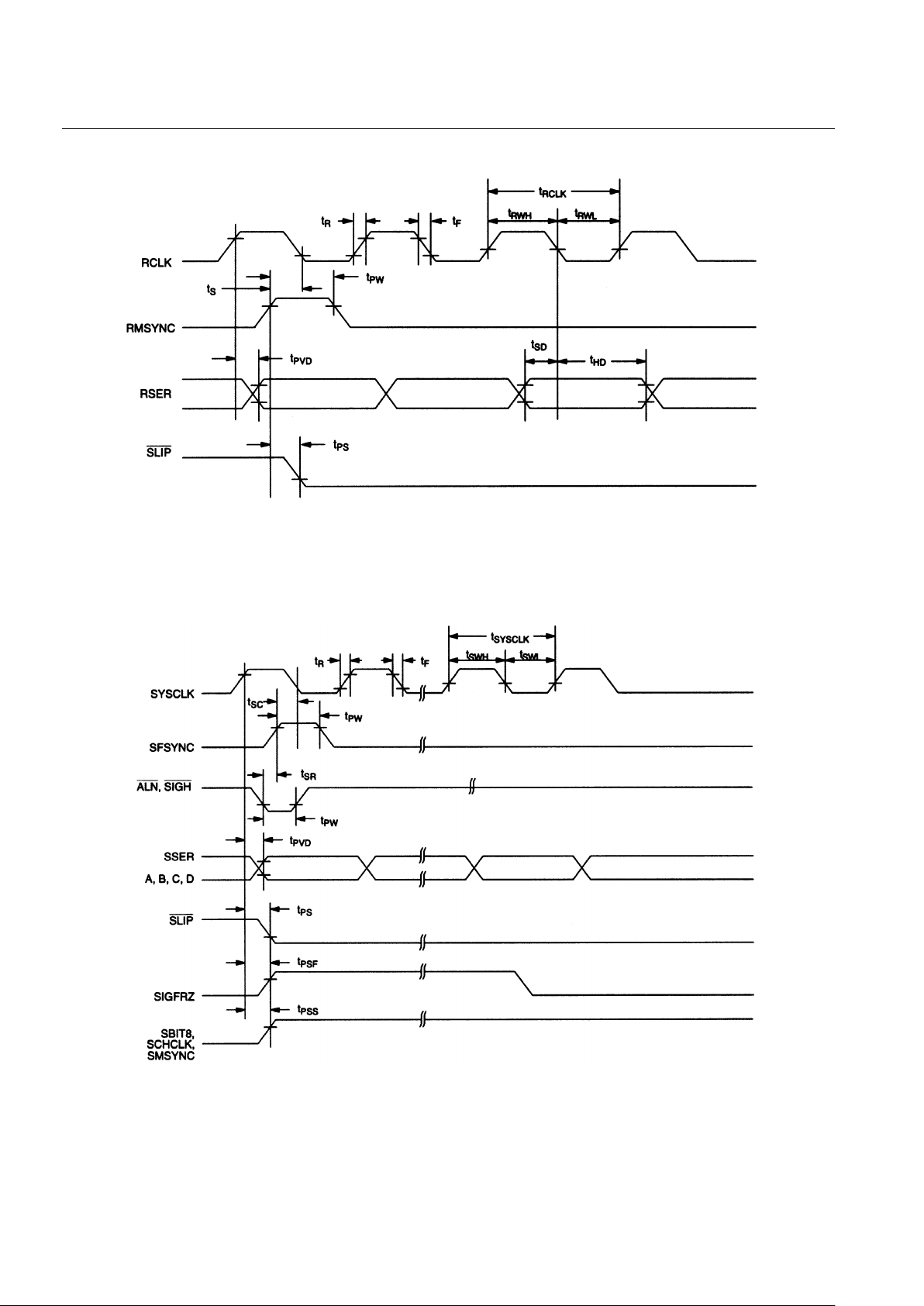
RECEIVE AC DIAGRAM Figure 9
SYSTEM AC TIMING DIAGRAM Figure 10

DS2176
13 of 15
DS2176 T1 RECEIVE BUFFER
PKG 24-PIN
DIM MIN MAX
A IN.
MM
1.245 1.265
B IN.
MM
0.250 0.270
C IN.
MM
0.125 0.145
D IN.
MM
0.300 0.325
E IN.
MM
0.015 0.040
F IN.
MM
0.125 0.135
G IN.
MM
0.090 0.110
H IN.
MM
0.325 0.420
J IN.
MM
0.008 0.012
K IN.
MM
0.015 0.022

DS2176
14 of 15
DS2176Q
INCHES
DIM
MIN MAX
A 0.165 0.180
A1 0.090 0.120
A2 0.020 -
B 0.026 0.033
B1 0.013 0.021
C 0.009 0.012
D 0.485 0.495
D1 0.450 0.456
D2 0.390 0.430
E 0.485 0.495
E1 0.450 0.456
E2 0.390 0.430
L1 0.060 -
N 28 -
e1 0.050 BSC
CH1 0.042 0.048

DS2176
15 of 15
DATA SHEET REVISION SUMMARY
The following represent the key differences between 04/19/95 and 06/13/97 version of the DS2176 data
sheet. Please review this summary carefully.
1. SYNC/CLOCK Relationship in timing diagram
 Loading...