

dallas semiconductor DS2151Q service manual
DS2151Q
T1 Single-Chip Transceiver
www.dalsemi.com
STORES
INTERFACE
CSRDAD7
AD6
AD5
AD4
AD3
AD2
AD1
AD0
TCHCLK
1234564443424140
15
1819202122232425262728
33
查询DS2151供应商
FEATURES
§ Complete DS1/ISDN-PRI transceiver
functionality
§ Line interface can handle both long- and
short-haul trunks
§ 32-bit or 128-bit jitter attenuator
§ Generates DSX-1 and CSU line build outs
§ Frames to D4, ESF, and SLC-96
§ Dual onboard two-frame elastic store slip
buffers that connect to backplanes up to 8.192
MHz
§ 8-bit parallel control port that can be used on
either multiplexed or non-multiplexed buses
§ Extracts and inserts Robbed-Bit signaling
§ Detects and generates yellow and blue alarms
§ Programmable output clocks for Fractional T1
§ Fully independent transmit and receive
functionality
§ Onboard FDL support circuitry
§ Generates and detects CSU loop codes
§ Contains ANSI one’s density monitor and
enforcer
§ Large path and line error counters including
BPV, CV, CRC6, and framing bit errors
§ Pin compatible with DS2153Q E1 Single-
Chip Transceiver
§ 5V supply; low power CMOS
§ Industrial grade version (-40°C to +85°C)
available (DS2151QN)
R
formats
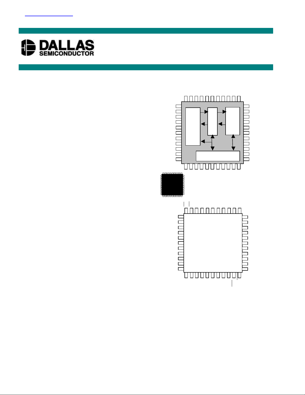
PIN ASSIGNMENT
FUNCTIONAL BLOCKS
HAUL LINE
LONG & SHORT
PARALLEL CONTROL
Dallas
DS2151Q
T1SCT
ALE
WR
RLINK
RLCLK
DVSS
RCLK
RCHCLK
RSER
RSYNC
RLOS/LOTC
SYSCLK
ACTUAL SIZE OF 44-PIN PLCC
7
8
9
10
11
12
13
14
16
17
FRAMER
PORT
ELASTIC
39
38
37
36
35
34
32
31
30
29
TSER
TCLK
DVDD
TSYNC
TLINK
TLCLK
TCHBLK
TRING
TVDD
TVSS
TTIP
DESCRIPTION
The DS2151Q T1 Single-Chip Transceiver (SCT) contains all of the necessary functions for connection
to T1 lines whether they be DS-1 long haul or DSX-1 short haul. The clock recovery circuitry
automatically adjusts to T1 lines from 0 feet to over 6000 feet in length. The device can generate both
DSX-1 line build outs as well as CSU build outs of -7.5 dB, -15 dB, and -22.5 dB. The onboard jitter
attenuator (selectable to either 32 bits or 128 bits) can be placed in either the transmit or receive data
paths. The framer locates the frame and multiframe boundaries and monitors the data stream for alarms.
It is also used for extracting and inserting Robbed-Bit signaling data and FDL data. The device contains
a set of 64 8-bit internal registers which the user can access to control the operation of the unit. Quick
access via the parallel control port allows a single micro to handle many T1 lines. The device fully meets
all of the latest T1 specifications including ANSI T1.403-199X, AT&T TR 62411 (12-90), and ITU
G.703, G.704, G.706, G.823, and I.431.
ACLKI
RCHBLK
BTS
RTIP
RVDD
RRING
RVSS
XTAL1
XTAL2
INT1
INT2
1 of 51 081099

TABLE OF CONTENTS
1. Introduction
2. Parallel Control Port
3. Control Registers
4. Status and Information Registers
5. Error Count Registers
6. FDL/Fs Extraction/Insertion
7. Signaling Operation
8. Transmit Transparency and Idle Registers
9. Clock Blocking Registers
10. Elastic Stores Operation
DS2151Q
11. Receive Mark Registers
12. Line Interface Functions
13. Timing Diagrams and Transmit Flow Diagram
14. DC and AC Characteristics
1.0 INTRODUCTION
The analog AMI waveform off of the T1 line is transformer coupled into the RRING and RTIP pins of
the DS2151Q. The device recovers clock and data from the analog signal and passes it through the jitter
attenuation mux to the receive side framer where the digital serial stream is analyzed to locate the framing
pattern. If needed, the receive side elastic store can be enabled in order to absorb the phase and frequency
differences between the recovered T1 data stream and an asynchronous backplane clock which is
provided at the SYSCLK input.
The transmit side of the DS2151Q is totally independent from the receive side in both the clock
requirements and characteristics. Data can be either provided directly to the transmit formatter or via an
elastic store. The transmit formatter will provide the necessary data overhead for T1 transmission. Once
the data stream has been prepared for transmission, it is sent via the jitter attenuation mux to the
waveshaping and line driver functions. The DS2151Q will drive the T1 line from the TTIP and TRING
pins via a coupling transformer.
2 of 51
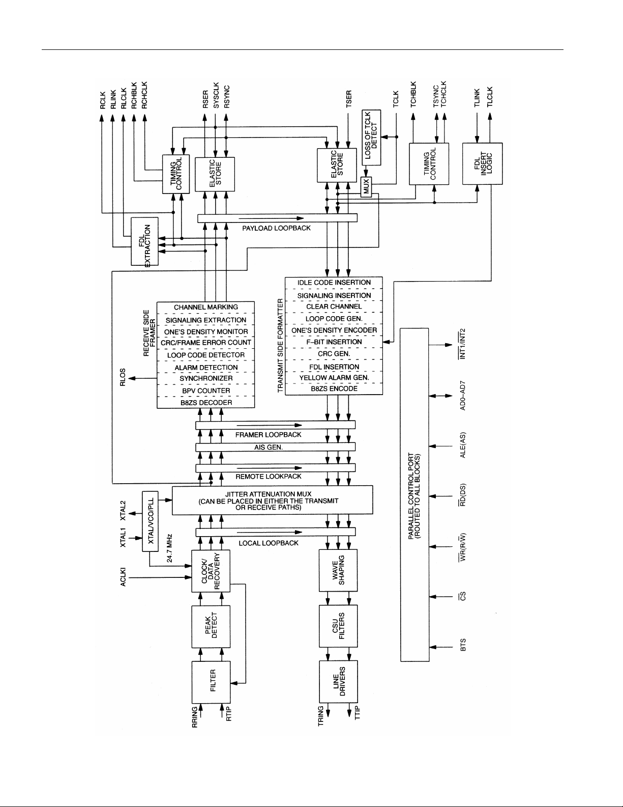
DS2151Q BLOCK DIAGRAM Figure 1-1
DS2151Q
3 of 51

DS2151Q
RD
PIN DESCRIPTION Table 1-1
PIN SYMBOL TYPE DESCRIPTION
1
2
3
4
5
6
7 ALE(AS) I Address Latch Enable (Address Strobe). A positive going edge
8
9 RLINK O Receive Link Data. Updated with either FDL data (ESF) or Fs bits
10 RLCLK O Receive Link Clock. 4 kHz or 2 kHz (ZBTSI) demand clock for the
11 DVSS - Digital Signal Ground. 0.0 volts. Should be tied to local ground plane.
12 RCLK O Receive Clock. Recovered 1.544 MHz clock.
13 RCHCLK O Receive Channel Clock. 192 kHz clock which pulses high during the
14 RSER O Receive Serial Data. Received NRZ serial data, updated on rising
15 RSYNC I/O Receive Sync. An extracted pulse, one RCLK wide, is output at this
16 RLOS/LOTC O Receive Loss of Sync/Loss of Transmit Clock. A dual function
17 SYSCLK I System Clock. 1.544 MHz or 2.048 MHz clock. Only used when the
18 RCHBLK O Receive Channel Block. A user programmable output that can be
AD4
AD5
AD6
AD7
(DS)
CS
WR (R/W )
I/O Address/Data Bus. An 8-bit multiplexed address/data bus.
I
Read Input (Data Strobe).
I Chip Select. Must be low to read or write the port.
serves to demultiplex the bus.
I
Write Input (Read/Write).
(D4) or Z bits (ZBTSI) one RCLK before the start of a frame. See
Section 13 for timing details.
RLINK output. See Section 13 for timing details.
LSB of each channel. Useful for parallel to serial conversion of channel
data, locating Robbed-Bit signaling bits, and for blocking clocks in
DDS applications. See Section 13 for timing details.
edges of RCLK or SYSCLK.
pin which identifies either frame (RCR2.4=0) or multiframe boundaries
(RCR2.4=1). If set to output frame boundaries, then via RCR2.5,
RSYNC can also be set to output double-wide pulses on signaling
frames. If the elastic store is enabled via the CCR1.2, then this pin can
be enabled to be an input via RCR2.3 at which a frame boundary pulse
is applied. See Section 13 for timing details.
output. If CCR3.5=0, will toggle high when the synchronizer is
searching for the T1 frame and multiframe; if CCR3.5=1, will toggle
high if the TCLK pin has not toggled for 5 us.
elastic store functions are enabled via either CCR1.7 or CCR1.2.
Should be tied low in applications that do not use the elastic store. If
tied high for more than 100 us, will force all output pins (including the
parallel port) to 3-state.
forced high or low during any of the 24 T1 channels. Useful for
blocking clocks to a serial UART or LAPD controller in applications
where not all T1 channels are used such as Fractional T1, 384k bps
service, 768k bps, or ISDN-PRI. Also useful for locating individual
channels in drop-and-insert applications. See Section 13 for timing
details.
4 of 51

DS2151Q
PIN SYMBOL TYPE DESCRIPTION
19 ACLKI I Alternate Clock Input. Upon a receive carrier loss, the clock applied at
this pin (normally 1.544 MHz) will be routed to the RCLK pin. If no
clock is routed to this pin, then it should be tied to DVSS VIA A1K Ohm
RESISTOR.
20 BTS I Bus Type Select. Strap high to select Motorola bus timing; strap low to
select Intel bus timing. This pin controls the function of the RD(DS),
ALE(AS), and WR (R/ W ) pins. If BTS=1, then these pins assume the
function listed in parenthesis ().
21
22
RTIP
RRING
- Receive Tip and Ring. Analog inputs for clock recovery circuitry;
connects to a 1:1 transformer (see Section 12 for details).
23 RVDD - Receive Analog Positive Supply. 5.0 volts. Should be tied to DVDD
and TVDD pins.
24 RVSS - Receive Signal Ground. 0.0 volts. Should be tied to local ground plane
25
26
XTAL1
XTAL2
- Crystal Connections. A pullable 6.176 MHz crystal must be applied to
these pins. See Section 12 for crystal specifications.
27
INT1
O Receive Alarm Interrupt 1. Flags host controller during alarm
conditions defined in Status Register 1. Active low, open drain output.
28
INT2
O Receive Alarm Interrupt 2. Flags host controller during conditions
defined in Status Register 2. Active low, open drain output.
29 TTIP - Transmit Tip. Analog line driver output; connects to a step-up
transformer (see Section 12 for details).
30 TVSS - Transmit Signal Ground. 0.0 volts. Should be tied to local ground
plane.
31 TVDD - Transmit Analog Positive Supply. 5.0 volts. Should be tied to DVDD
and RVDD pins.
32 TRING - Transmit Ring. Analog line driver outputs; connects to a step-up
transformer (see Section 12 for details).
33 TCHBLK O Transmit Channel Block. A user programmable output that can be
forced high or low during any of the 24 T1 channels. Useful for blocking
clocks to a serial UART or LAPD controller in applications where not all
T1 channels are used such as Fractional T1, 384k bps service, 768k bps,
or ISDN-PRI. Also useful for locating individual channels in drop-and-
insert applications. See Section 13 for timing details.
34 TLCLK O Transmit Link Clock. 4 kHz or 2 kHz (ZBTSI) demand clock for the
TLINK input. See Section 13 for timing details.
35 TLINK I Transmit Link Data. If enabled via TCR1.2, this pin will be sampled
during the F-bit time on the falling edge of TCLK for data insertion into
either the FDL stream (ESF) or the Fs bit position (D4) or the Z-bit
position (ZBTSI). See Section 13 for timing details.
36 TSYNC I/O Transmit Sync. A pulse at this pin will establish either frame or
multiframe boundaries for the DS2151Q. Via TCR2.2, the DS2151Q can
be programmed to output either a frame or multiframe pulse at this pin. If
this pin is set to output pulses at frame boundaries, it can also be set via
TCR2.4 to output double-wide pulses at signaling frames. See Section 13
for timing details.
37 DVDD - Digital Positive Supply. 5.0 volts. Should be tied to RVDD and TVDD
pins.
5 of 51
DS2151Q
PIN SYMBOL TYPE DESCRIPTION
38 TCLK I Transmit Clock. 1.544 MHz primary clock.
39 TSER I Transmit Serial Data. Transmit NRZ serial data, sampled on the falling edge
of TCLK.
40 TCHCLK O Transmit Channel Clock. 192 kHz clock which pulses high during the LSB
of each channel. Useful for parallel to serial conversion of channel data,
locating Robbed-Bit signaling bits, and for blocking clocks in DDS applica-
tions. See Section 13 for timing details.
41
42
43
44
AD0
AD1
AD2
AD3
I/O Address/Data Bus. An 8-bit multiplexed address/data bus.
DS2151Q REGISTER MAP
ADDRESS R/W REGISTER NAME ADDRESS R/W REGISTER NAME
20 R/W Status Register 1. 30 R/W Common Control Register 3.
21 R/W Status Register 2. 31 R/W Receive Information Register 2.
22 R/W Receive Information Register 1. 32 R/W Transmit Channel Blocking Register 1.
23 R Line code Violation Count
Register 1.
24 R Line code Violation Count
Register 2.
25 R Path Code Violation Count
Register 1. (1)
26 R Path Code Violation Count
Register 2.
27 R Multiframe Out of Sync Count
Register 2.
28 R Receive FDL Register. 38 R/W Common Control Register 2.
29 R/W Receive FDL Match Register 1. 39 R/W Transmit Transparency Register 1.
2A R/W Receive FDL Match Register 2. 3A R/W Transmit Transparency Register 2.
2B R/W Receive Control Register 1. 3B R/W Transmit Transparency Register 3.
2C R/W Receive Control Register 2. 3C R/W Transmit Idle Register 1.
2D R/W Receive Mark Register 1. 3D R/W Transmit Idle Register 2.
2E R/W Receive Mark Register 2. 3E R/W Transmit Idle Register 3.
2F R/W Receive Mark Register 3. 3F R/W Transmit Idle Definition Register.
60 R Receive Signaling Register 1. 70 R/W Transmit Signaling Register 1.
61 R Receive Signaling Register 2. 71 R/W Transmit Signaling Register 2.
62 R Receive Signaling Register 3. 72 R/W Transmit Signaling Register 3.
33 R/W Transmit Channel Blocking Register 2.
34 R/W Transmit Channel Blocking Register 3.
35 R/W Transmit Control Register 1.
36 R/W Transmit Control Register 2.
37 R/W Common Control Register 1.
6 of 51
DS2151Q REGISTER MAP (continued)
63 R Receive Signaling Register 4. 73 R/W Transmit Signaling Register 4.
64 R Receive Signaling Register 5. 74 R/W Transmit Signaling Register 5.
65 R Receive Signaling Register 6. 75 R/W Transmit Signaling Register 6.
66 R Receive Signaling Register 7. 76 R/W Transmit Signaling Register 7.
67 R Receive Signaling Register 8. 77 R/W Transmit Signaling Register 8.
68 R Receive Signaling Register 9. 78 R/W Transmit Signaling Register 9.
69 R Receive Signaling Register 10. 79 R/W Transmit Signaling Register 10.
6A R Receive Signaling Register 11. 7A R/W Transmit Signaling Register 11.
6B R Receive Signaling Register 12. 7B R/W Transmit Signaling Register 12.
6C R/W Receive Channel Blocking
Register 1.
6D R/W Receive Channel Blocking
Register 2.
6E R/W Receive Channel Blocking
Register 3.
6F R/W Interrupt Mask Register 2. 7F R/W Interrupt Mask Register 1.
7C R/W Line Interface Control Register.
7D R/W Test Register. (2)
7E R/W Transmit FDL Register.
DS2151Q
NOTES:
1. Address 25 also contains Multiframe Out of Sync Count Register 1.
2. The Test Register is used only by the factory; this register must be cleared (set to all 0s) on power-up
initialization to insure proper operation.
2.0 PARALLEL PORT
The DS2151Q is controlled via a multiplexed bidirectional address/data bus by an external
microcontroller or microprocessor. The DS2151Q can operate with either Intel or Motorola bus timing
configurations. If the BTS pin is tied low, Intel timing will be selected; if tied high, Motorola timing will
be selected. All Motorola bus signals are listed in parenthesis (). See the timing diagrams in the A.C.
Electrical Characteristics for more details. The multiplexed bus on the DS2151Q saves pins because the
address information and data information share the same signal paths. The addresses are presented to the
pins in the first portion of the bus cycle and data will be transferred on the pins during second portion of
the bus cycle. Addresses must be valid prior to the falling edge of ALE (AS), at which time the
7 of 51

DS2151Q
DS2151Q latches the address from the AD0 to AD7 pins. Valid write data must be present and held
stable during the later portion of the DS or WR pulses. In a read cycle, the DS2151Q outputs a byte of
data during the latter portion of the DS or RD pulses. The read cycle is terminated and the bus returns to
a high impedance state as RD transitions high in Intel timing or as DS transitions low in Motorola timing.
The DS2151Q can also be easily connected to non-multiplexed buses. Please see the separate Application
Note for a detailed discussion of this topic.
3.0 CONTROL REGISTERS
The operation of the DS2151Q is configured via a set of eight registers. Typically, the control registers
are only accessed when the system is first powered up. Once the DS2151Q has been initialized, the
control registers will only need to be accessed when there is a change in the system configuration. There
are two Receive Control Registers (RCR1 and RCR2), two Transmit Control Registers (TCR1 and
TCR2), a Line Interface Control Register (LICR), and three Common Control Registers (CCR1, CCR2,
and CCR3). Seven of the eight registers are described below. The LICR is described in Section 12.
RCR1: RECEIVE CONTROL REGISTER 1 (Address=2B Hex)
(MSB) (LSB)
LCVCRF ARC OOF1 OOF2 SYNCC SYNCT SYNCE RESYNC
SYMBOL POSITION NAME AND DESCRIPTION
LCVCRF RCR1.7
Line Code Violation Count Register Function Select.
0=do not count excessive 0s
1=count excessive 0s
ARC RCR1.6
OOF1 RCR1.5
OOF2 RCR1.4
SYNCC RCR1.3
SYNCT RCR1.2 Sync Time.
Auto Resync Criteria.
0=Resync on OOF or RCL event
1=Resync on OOF only
Out Of Frame Select 1.
0=2/4 frame bits in error
1=2/5 frame bits in error
Out Of Frame Select 2.
0=follow RCR1.5
1=2/6 frame bits in error
Sync Criteria.
In D4 Framing Mode
0=search for Ft pattern, then search for Fs pattern
1=cross couple Ft and Fs pattern
In ESF Framing Mode
0=search for FPS pattern only
1=search for FPS and verify with CRC6
0=qualify 10 bits
1=qualify 24 bits
8 of 51

SYNCE RCR1.1 Sync Enable.
Resync
0=auto resync enabled
1=auto resync disabled
DS2151Q
RESYNC RCR1.0
of the receive side framer is initiated. Must be cleared and set
again for a subsequent resync.
. When toggled from low to high, a resynchronization
RCR2: RECEIVE CONTROL REGISTER 2 (Address=2C Hex)
(MSB) (LSB)
RCS RZBTSI RSDW RSM RSIO RD4YM FSBE MOSCRF
SYMBOL POSITION NAME AND DESCRIPTION
RCS RCR2.7
RZBTSI RCR2.6
RSDW RCR2.5
Receive Code Select.
0=idle code (7F Hex)
1=digital milliwatt code (1E/0B/0B/1E/9E/8B/8B/9E Hex)
Receive Side ZBTSI Enable.
0=ZBTSI disabled
1=ZBTSI enabled
RSYNC Double-Wide.
0=do not pulse double-wide in signaling frames
1=do pulse double-wide in signaling frames (note: this bit must
be set to 0 when RCR2.4=1 or when RCR2.3=1)
RSM RCR2.4
RSIO RCR2.3
RD4YM RCR2.2
FSBE RCR2.1
MOSCRF RCR2.0
RSYNC Mode Select.
0=frame mode (see the timing in Section 13)
1=multiframe mode (see the timing in Section 13)
RSYNC I/O Select.
0=RSYNC is an output
1=RSYNC is an input (only valid if elastic store enabled) (note:
this bit must be set to 0 when CCR1.2=0)
Receive Side D4 Yellow Alarm Select.
0=0s in bit 2 of all channels
1=a 1 in the S-bit position of frame 12
PCVCR Fs Bit Error Report Enable.
0=do not report bit errors in Fs bit position; only Ft bit position
1=report bit errors in Fs bit position as well as Ft bit position
Multiframe Out of Sync Count Register Function Select.
0=count errors in the framing bit position
1=count the number of multiframes out of sync
TCR1: TRANSMIT CONTROL REGISTER 1 (Address=35 Hex)
(MSB) (LSB)
LOTCMC TFPT TCPT RBSE GB7S TLINK TBL TYEL
SYMBOL POSITION NAME AND DESCRIPTION
9 of 51

LOTCMC TCR1.7
Loss Of Transmit Clock Mux Control
. Determines whether
the transmit side formatter should switch to the ever present
RCLK if the TCLK input should fail to transition (see Figure 11 for more details).
0=do not switch to RCLK if TCLK stops
1=switch to RCLK if TCLK stops
TFPT TCR1.6 Transmit Framing Pass Through. (see note below)
0=Ft or FPS bits sourced internally
1=Ft or FPS bits sampled at TSER during F-bit time
TCPT TCR1.5 Transmit CRC Pass Through. (see note below)
0=source CRC6 bits internally
1=CRC6 bits sampled at TSER during F-bit time
RBSE TCR1.4 Robbed-Bit Signaling Enable. (see note below)
0=no signaling is inserted in any channel
1=signaling is inserted in all channels (the TTR registers can be
used to block insertion on a channel by channel basis)
DS2151Q
GB7S TCR1.3 Global Bit 7 Stuffing. (see note below)
0=allow the TTR registers to determine which channels
containing all 0s are to be Bit 7 stuffed
1=force Bit 7 stuffing in all 0 byte channels regardless of how
the TTR registers are programmed
TLINK TCR1.2 TLINK Select. (see note below)
0=source FDL or Fs bits from TFDL register
1=source FDL or Fs bits from the TLINK pin
TBL TCR1.1 Transmit Blue Alarm. (see note below)
0=transmit data normally
1=transmit an unframed all 1s code at TPOS and TNEG
TYEL TCR1.0 Transmit Yellow Alarm. (see note below)
0=do not transmit yellow alarm
1=transmit yellow alarm
Note: for a detailed description of how the bits in TCR1 affect the transmit side formatter of the
DS2151Q, please see Figure 13-9.
10 of 51

TCR2: TRANSMIT CONTROL REGISTER 2 (Address=36 Hex)
TSYNC Double-Wide.
(MSB) (LSB)
TEST1 TEST0 TZBTSI TSDW TSM TSIO TD4YM B7ZS
SYMBOL POSITION NAME AND DESCRIPTION
TEST1 TCR2.7
Test Mode Bit 1 for Output Pins. See Table 3-1.
DS2151Q
TEST0 TCR2.6
TZBTSI TCR2.5 Transmit Side ZBTSI Enable.
TSDW TCR2.4
TSM TCR2.3
TSIO TCR2.2 TSYNC I/O Select.
TD4YM TCR2.1
Test Mode Bit 0 for Output Pins. See Table 3-1.
0=ZBTSI disabled
1=ZBTSI enabled
(note: this bit must be set to 0 when
TCR2.3=1 or when TCR2.2=0)
0=do not pulse double-wide in signaling frames
1=do pulse double-wide in signaling frames
TSYNC Mode Select.
0=frame mode (see the timing in Section 13)
1=multiframe mode (see the timing in Section 13)
0=TSYNC is an input
1=TSYNC is an output
Transmit Side D4 Yellow Alarm Select.
0=0s in bit 2 of all channels
1=a 1 in the S-bit position of frame 12
B7ZS XTCR2.0
Bit 7 0 Suppression Enable.
0=no stuffing occurs
1=Bit 7 force to a 1 in channels with all 0s
OUTPUT PIN TEST MODES Table 3-1
TEST1 TEST0 EFFECT ON OUTPUT PINS
0 0 operate normally
0 1 force all output pins 3-state (including all I/O pins and parallel port pins)
1 0 force all output pins low (including all I/O pins except parallel port pins)
1 1 force all output pins high (including all I/O pins except parallel port pins)
11 of 51

CCR1: COMMON CONTROL REGISTER 1 (Address=37 Hex)
(MSB) (LSB)
TESE LLB RSAO RLB SCLKM RESE PLB FLB
SYMBOL POSITION NAME AND DESCRIPTION
TESE CCR1.7
Transmit Elastic Store Enable.
0=elastic store is bypassed
1=elastic store is enabled
DS2151Q
LLB CCR1.6
RSAO CCR1.5
RLB CCR1.4
SCLKM CCR1.3
RESE CCR1.2
PLB CCR1.1
Local Loopback.
0=loopback disabled
1=loopback enabled
Receive Signaling All 1s.
0=allow robbed signaling bits to appear at RSER
1=force all robbed signaling bits at RSER to 1
Remote Loopback.
0=loopback disabled
1=loopback enabled
SYSCLK Mode Select.
0=if SYSCLK is 1.544 MHz
1=if SYSCLK is 2.048 MHz
Receive Elastic Store Enable.
0=elastic store is bypassed
1=elastic store is enabled
Payload Loopback.
0=loopback disabled
1=loopback enabled
FLB CCR1.0
Framer Loopback.
0=loopback disabled
1=loopback enabled
LOCAL LOOPBACK
When CCR1.6 is set to a 1, the DS2151Q will be forced into Local LoopBack (LLB). In this loopback,
data will continue to be transmitted as normal through the transmit side of the SCT. Data being received
at RTIP and RRING will be replaced with the data being transmitted. Data in this loopback will pass
through the jitter attenuator and the jitter attenuator should be programmed to be in the transmit path.
LLB is primarily used in debug and test applications. Please see the DS2151Q Block Diagram in Section
1 for more details.
REMOTE LOOPBACK
When CCR1.4 is set to a 1, the DS2151Q will be forced into Remote LoopBack (RLB). In this loopback,
data recovered off the T1 line from the RTIP and RRING pins will be transmitted back onto the T1 line
12 of 51

DS2151Q
(with any BPVs that might have occurred intact) via the TTIP and TRING pins. Data will continue to
pass through the receive side of the DS2151Q as it would normally and the data at the TSER input will be
ignored. Data in this loopback will pass through the jitter attenuator. RLB is used to place the DS2151Q
into “line” loopback which is a requirement of both ANSI T1.403 and AT&T TR62411. Please see the
DS2151Q Block Diagram in Section 1 for more details.
PAYLOAD LOOPBACK
When CCR1.1 is set to a 1, the DS2151Q will be forced into Payload LoopBack (PLB). Normally, this
loopback is only enabled when ESF framing is being performed. In a PLB situation, the DS2151Q will
loop the 192 bits of payload data (with BPVs corrected) from the receive section back to the transmit
section. The FPS framing pattern, CRC6 calculation, and the FDL bits are not looped back, they are
reinserted by the DS2151Q. When PLB is enabled, the following will occur:
1. Data will be transmitted from the TTIP and TRING pins synchronous with RCLK instead of TCLK.
2. All of the receive side signals will continue to operate normally.
3. The TCHCLK and TCHBLK signals are forced low.
4. Data at the TSER pin is ignored.
5. The TLCLK signal will become synchronous with RCLK instead of TCLK.
FRAMER LOOPBACK
When CCR1.0 is set to a 1, the DS2151Q will enter a Framer LoopBack (FLB) mode. This loopback is
useful in testing and debugging applications. In FLB, the DS2151Q will loop data from the transmit side
back to the receive side. When FLB is enabled, the following will occur:
1. Unless the RLB is active, an unframed all 1s code will be transmitted at TTIP and TRING.
2. Data off the T1 line at RTIP and RRING will be ignored.
3. The RCLK output will be replaced with the TCLK input.
13 of 51

CCR2: COMMON CONTROL REGISTER 2 (Address=38 Hex)
(MSB) (LSB)
TFM TB8ZS TSLC96 TFDL RFM RB8ZS RSLC96 RFDL
SYMBOL POSITION NAME AND DESCRIPTION
TFM CCR2.7
Transmit Frame Mode Select.
0=D4 framing mode
1=ESF framing mode
DS2151Q
TB8ZS CCR2.6
TSLC96 CCR2.5
TFDL CCR2.4
RFM CCR2.3
RB8ZS CCR2.2
RSLC96 CCR2.1
Transmit B8ZS Enable.
0=B8ZS disabled
1=B8ZS enabled
Transmit SLC-96/Fs Bit Loading Enable.
0=SLC-96/Fs bit Loading disabled
1=SLC-96/Fs bit Loading enabled
Transmit FDL 0 Stuffer Enable.
0=0 stuffer disabled
1=0 stuffer enabled
Receive Frame Mode Select.
0=D4 framing mode
1=ESF framing mode
Receive B8ZS Enable.
0=B8ZS disabled
1=B8ZS enabled
Receive SLC-96 Enable.
0=SLC-96 disabled
1=SLC-96 enabled
RFDL CCR2.0
Receive FDL 0 Destuffer Enable.
0=0 destuffer disabled
1=0 destuffer enabled
14 of 51

DS2151Q
Elastic Store Minimum Delay Mode.
Elastic Store Reset.
RSYNC Multiframe Skip Control.
Line Interface Reset.
CCR3: COMMON CONTROL REGISTER 3 (Address=30 Hex)
(MSB) (LSB)
ESMDM ESR P16F RSMS PDE TLD TLU LIRST
SYMBOL POSITION NAME AND DESCRIPTION
ESMDM CCR3.7
details.
0=elastic stores operate at full two-frame depth
1=elastic stores operate at 32-bit depth
See Section 10.3 for
ESR CCR3.6
P16F CCR3.5
RSMS CCR3.4
PDE CCR3.3
TLD CCR3.2
Setting this bit from a 0 to a 1 will force
the elastic stores to a known depth. Should be toggled after
SYSCLK has been applied and is stable. Must be cleared and
set again for a subsequent reset.
Function of Pin 16.
0=Receive Loss of Sync (RLOS).
1=Loss of Transmit Clock (LOTC).
Useful in framing format
conversions from D4 to ESF.
0=RSYNC will output a pulse at every multiframe
1=RSYNC will output a pulse at every other multiframe note:
for this bit to have any affect, the RSYNC must be set to output
multiframe pulses (RCR2.4=1 and RCR2.3=0) and the receive
elastic store must be bypassed. (CCR1.2 = 0).
Pulse Density Enforcer Enable.
0=disable transmit pulse density enforcer
1=enable transmit pulse density enforcer
Transmit Loop Down Code (001).
0=transmit data normally
1=replace normal transmitted data with Loop Down code
TLU CCR3.1
LIRST CCR3.0
LOOP CODE GENERATION
When either the CCR3.1 or CCR3.2 bits are set to 1, the DS2151Q will replace the normal transmitted
payload with either the Loop Up or Loop Down code respectively. The DS2151Q will overwrite the
repeating loop code pattern with the framing bits. The SCT will continue to transmit the loop codes as
long as either bit is set. It is an illegal state to have both CCR3.1 and CCR3.2 set to 1 at the same time.
Transmit Loop Up Code (00001).
0=transmit data normally
1=replace normal transmitted data with Loop Up code
Setting this bit from a 0 to a one will
initiate an internal reset that affects the slicer, AGC, clock
recovery state machine and jitter attenuator. Normally this bit is
only toggled on power-up. Must be cleared and set again for a
subsequent reset.
15 of 51

DS2151Q
PULSE DENSITY ENFORCER
The SCT always examines both the transmit and receive data streams for violations of the following rules
which are required by ANSI T1.403-199X:
– no more than 15 consecutive 0s
– at least N 1s in each and every time window of 8 x (N +1) bits where N=1 through 23
Violations for the transmit and receive data streams are reported in the RIR2.0 and RIR2.1 bits
respectively.
When the CCR3.3 is set to 1, the DS2151Q will force the transmitted stream to meet this requirement no
matter the content of the transmitted stream. When running B8ZS, the CCR3.3 bit should be set to 0,
since B8ZS encoded data streams cannot violate the pulse density requirements.
POWER-UP SEQUENCE
On power-up, after the supplies are stable, the DS2151Q should be configured for operation by writing to
all of the internal registers (this includes setting the Test Register to 00Hex) since the contents of the
internal registers cannot be predicted on power-up. Next, the LIRST bit should be toggled from 0 to 1 to
reset the line interface (it will take the DS2151Q about 40 ms to recover from the LIRST being toggled).
Finally, after the SYSCLK input is stable, the ESR bit should be toggled from a 0 to a 1 (this step can be
skipped if the elastic stores are disabled).
4.0 STATUS AND INFORMATION REGISTERS
There is a set of four registers that contain information on the current real time status of the DS2151Q:
Status Register 1 (SR1), Status Register 2 (SR2), Receive Information Register 1 (RIR1), and Receive
Information Register 2 (RIR2). When a particular event has occurred (or is occurring), the appropriate bit
in one of these four registers will be set to a 1. All of the bits in these registers operate in a latched
fashion. This means that if an event occurs and a bit is set to a 1 in any of the registers, it will remain set
until the user reads that bit. The bit will be cleared when it is read and it will not be set again until the
event has occurred again or if the alarm(s) is still present.
The user will always precede a read of these registers with a write. The byte written to the register will
inform the DS2151Q which bits the user wishes to read and have cleared. The user will write a byte to
one of these four registers, with a 1 in the bit positions he or she wishes to read and a 0 in the bit positions
he or she does not wish to obtain the latest information on. When a 1 is written to a bit location, the read
register will be updated with current value and the previous value will be cleared. When a 0 is written to
a bit position, the read register will not be updated and the previous value will be held. A write to the
status and information registers will be immediately followed by a read of the same register. The read
result should be logically AND’ed with the mask byte that was just written and this value should be
written back into the same register to insure that the bit does indeed clear. This second write is necessary
because the alarms and events in the status registers occur asynchronously in respect to their access via
the parallel port. The write-read-write scheme is unique to the four status registers and it allows an
external microcontroller or microprocessor to individually poll certain bits without disturbing the other
bits in the register. This operation is key in controlling the DS2151Q with higher-order software
languages.
The SR1 and SR2 registers have the unique ability to initiate a hardware interrupt via the INT1 and INT2
pins respectively. Each of the alarms and events in the SR1 and SR2 can be either masked or unmasked
16 of 51
 Loading...