Dallas Semiconductor DS21Q348N, DS21Q348, DS21348TN, DS21348T, DS21348GN Datasheet
...
www.maxim-ic.com
DS21348/Q348
3.3V E1/T1/J1 Line Interface
FEATURES
§ Complete E1, T1, or J1 line interface unit
(LIU)
§ Supports both long-haul and short-haul
trunks
§ Internal software-selectable receive-side
termination for 75Ω/100Ω/120W
§ 3.3V power supply
§ 32-bit or 128-bit crystal-less jitter attenuator
requires only a 2.048MHz master clock for
both E1 and T1 with option to use 1.544MHz
for T1
§ Generates the appropriate line build-outs,
with and without return loss, for E1 and
DSX-1 and CSU line build-outs for T1
§ AMI, HDB3, and B8ZS, encoding/decoding
§ 16.384MHz, 8.192MHz, 4.096MHz, or
2.048MHz clock output synthesized to
recovered clock
§ Programmable monitor mode for receiver
§ Loopbacks and PRBS pattern generation/
detection with output for received errors
§ Generates/detects in-band loop codes, 1 to 16
bits including CSU loop codes
§ 8-bit parallel or serial interface with optional
hardware mode
§ Muxed and nonmuxed parallel bus supports
Intel or Motorola
§ Detects/generates blue (AIS) alarms
§ NRZ/bipolar interface for TX/RX data I/O
§ Transmit open-circuit detection
§ Receive Carrier Loss (RCL) indication
(G.775)
§ High-Z State for TTIP and TRING
§ 50mA (rms) current limiter
PIN DESCRIPTION
44
1
44 TQFP
7 mm
CABGA
ORDERING INFORMATION
DS21348TN 44-Pin TQFP (-40°C to +85°C)
DS21348T 44-Pin TQFP (0o C to +70oC)
DS21348GN 7mm CABGA (-40°C to +85°C)
DS21348G 7mm CABGA (0o C to +70oC)
DS21Q348N (Quad) BGA (-40°C to +85°C)
DS21Q348 (Quad) BGA (0o C to +70o C)
1 of 73 111501

DS21348/Q348
DESCRIPTION
The DS21348 is a complete selectable E1 or T1 LIU for short-haul and long-haul applications.
Throughout the data sheet, J1 is represented wherever T1 exists. Receive sensitivity adjusts automatically
to the incoming signal and can be programmed for 0dB to 12 dB or 0dB to 43dB for E1 applications and
0dB to 30dB or 0dB to 36dB for T1 applications. The device can generate the necessary G.703 E1
waveshapes in 75Ω or 120Ω applications and DSX-1 line build outs or CSU line build outs of 0dB,
-7.5dB, -15dB, and -22.5dB for T1 applications. The crystal-less onboard jitter attenuator requires only a
2.048MHz MCLK for both E1 and T1 applications (with the option of using a 1.544MHz MCLK in T1
applications). The jitter attenuator FIFO is selectable to either 32 bits or 128 bits in depth and can be
placed in either the transmit or receive data paths. An X 2.048MHz output clock synthesized to RCLK is
available for use as a backplane system clock (where n = 1, 2, 4, or 8). The DS21348 has diagnostic
capabilities such as loopbacks and PRBS pattern generation/detection. 16-bit loop-up and loop-down
codes can be generated and detected. The device can be controlled via an 8-bit parallel muxed or
nonmuxed port, serial port, or used in hardware mode. The device fully meets all of the latest E1 and T1
specifications including ANSI T1.403-1999, ANSI T1.408, AT&T TR 62411, ITU G.703, G.704, G.706,
G.736, G.775, G.823, I.431, O.151, O.161, ETSI ETS 300 166, JTG.703, JTI.431, JJ-20.1, TBR12,
TBR13, and CTR4.
2 of 73

DS21348/Q348
TABLE OF CONTENTS
1. LIST OF FIGURES............................................................................................................................... 4
2. LIST OF TABLES ................................................................................................................................ 5
3. INTRODUCTION................................................................................................................................. 6
3.1 DOCUMENT REVISION HISTORY ............................................................................................ 6
4. PIN DESCRIPTION .............................................................................................................................9
5. HARDWARE MODE ......................................................................................................................... 22
5.1 REGISTER MAP .......................................................................................................................... 23
5.2 PARALLEL PORT OPERATION................................................................................................ 23
5.3 SERIAL PORT OPERATION ...................................................................................................... 24
6. CONTROL REGISTERS.................................................................................................................... 24
6.1 DEVICE POWER-UP AND RESET............................................................................................ 31
7 STATUS REGISTERS .......................................................................................................................34
8. DIAGNOSTICS .................................................................................................................................. 39
8.1 IN-BAND LOOP CODE GENERATION AND DETECTION................................................... 39
8.2 LOOPBACKS ............................................................................................................................... 43
8.2.1 Remote Loopback (RLB)......................................................................................................... 43
8.2.2 Local Loopback (LLB)............................................................................................................ 43
8.2.3 Analog Loopback (LLB).......................................................................................................... 44
8.2.4 Dual Loopback (DLB) ............................................................................................................44
8.3 PRBS GENERATION & DETECTION....................................................................................... 44
8.4 ERROR COUNTER...................................................................................................................... 44
8.4.1 Error Counter Update ............................................................................................................ 45
8.5 ERROR INSERTION.................................................................................................................... 45
9. ANALOG INTERFACE..................................................................................................................... 46
9.1 RECEIVER..................................................................................................................................... 46
9.2 TRANSMITTER ........................................................................................................................... 47
9.3 JITTER ATTENUATOR ..............................................................................................................47
9.4 G.703 SYNCHRONIZATION SIGNAL ......................................................................................48
10. DS21Q348 QUAD LIU....................................................................................................................... 55
11. DC CHARACTERISTICS.................................................................................................................. 59
12. AC CHARACTERISTICS.................................................................................................................. 61
13. MECHANICAL DIMENSIONS......................................................................................................... 70
13.1 MECHANICAL DIMENSIONS—QUAD VERSION................................................................. 72
3 of 73

DS21348/Q348
1. LIST OF FIGURES
Figure 3-1 DS21348 BLOCK DIAGRAM................................................................................................... 7
Figure 3-2 RECEIVE LOGIC....................................................................................................................... 8
Figure 3-3 TRANSMIT LOGIC................................................................................................................... 9
Figure 4-1 PARALLEL PORT MODE PINOUT (BIS1 = 0, BIS0 = 1 or 0)............................................. 22
Figure 4-2 SERIAL PORT MODE PINOUT (BIS1 = 1, BIS0 = 0) .......................................................... 22
Figure 4-3 HARDWARE MODE PINOUT (BIS1 = 1, BIS0 = 1) ............................................................ 22
Figure 5-1 SERIAL PORT OPERATION FOR READ ACCESS (R=1) MODE 1.................................. 25
Figure 5-2 SERIAL PORT OPERATION FOR READ ACCESS MODE 2 ............................................. 25
Figure 5-3 SERIAL PORT OPERATION FOR READ ACCESS MODE 3 ............................................. 26
Figure 5-4 SERIAL PORT OPERATION FOR READ ACCESS MODE 4 ............................................. 26
Figure 5-5 SERIAL PORT OPERATION FOR WRITE ACCESS (R=0) MODES 1&2 ...……………27
Figure 5-6 SERIAL PORT OPERATION FOR WRITE ACCESS MODES 3& 4 …………...…………27
Figure 9-1 BASIC INTERFACE…………………………………………………………………………49
Figure 9-2 PROTECTED INTERFACE USING INTERNAL RECEIVE TERMINATION.................... 50
Figure 9-3 PROTECTED INTERFACE USING EXTERNAL RECEIVE TERMINATION................... 51
Figure 9-4 E1 TRANSMIT PULSE TEMPLATE...................................................................................... 52
Figure 9-5 T1 TRANSMIT PULSE TEMPLATE...................................................................................... 53
Figure 9-6 JITTER TOLERANCE............................................................................................................. 54
Figure 9-7 JITTER ATTENUATION ........................................................................................................ 54
Figure 10-1 BGA 12 x 12 PIN LAYOUT .................................................................................................. 58
Figure 12-1 INTEL BUS READ TIMING (PBTS = 0, BIS1 = 0, BIS0 = 0)............................................. 62
Figure 12-2 INTEL BUS WRITE TIMING (PBTS = 0, BIS1 = 0, BIS0 = 0)........................................... 62
Figure 12-3 MOTOROLA BUS TIMING (PBTS = 1, BIS1 = 0, BIS0 = 0) ............................................ 63
Figure 12-4 INTEL BUS READ TIMING (PBTS = 0, BIS1 = 0, BIS0 = 1)............................................. 65
Figure 12-5 INTEL BUS WRITE TIMING (PBTS = 0, BIS1 = 0, BIS0 = 1)........................................... 65
Figure 12-6 MOTOROLA BUS READ TIMING (PBTS = 1, BIS1 = 0, BIS0 = 1) ................................. 66
Figure 12-7 MOTOROLA BUS WRITE TIMING (PBTS = 1, BIS1 = 0, BIS0 = 1)................................ 66
Figure 12-8 SERIAL BUS TIMING (BIS1 = 1, BIS0 = 0)........................................................................ 67
Figure 12-9 RECEIVE SIDE TIMING ...................................................................................................... 68
Figure 12-10 TRANSMIT SIDE TIMING................................................................................................. 69
4 of 73

DS21348/Q348
2. LIST OF TABLES
Table 4-1 BUS INTERFACE SELECTION ................................................................................................ 9
Table 4-2a PIN ASSIGNMENT IN PARALLEL PORT MODE .............................................................. 10
Table 4-2b PIN DESCRIPTIONS IN PARALLEL PORT MODE (Sorted by Pin Name, DS21348T Pin
Numbering) .......................................................................................................................................... 11
Table 4-3a PIN ASSIGNMENT IN SERIAL PORT MODE..................................................................... 13
Table 4-3b PIN DESCRIPTIONS IN SERIAL PORT MODE (Sorted by Pin Name, DS21348T Pin
Numbering) .......................................................................................................................................... 14
Table 4-4a PIN ASSIGNMENT IN HARDWARE MODE....................................................................... 16
Table 4-4b PIN DESCRIPTIONS IN HARDWARE MODE (Sorted by Pin Name, DS21348T Pin
Numbering) .......................................................................................................................................... 17
Table 4-5 LOOPBACK CONTROL IN HARDWARE MODE ................................................................ 20
Table 4-6 TRANSMIT DATA CONTROL IN HARDWARE MODE ..................................................... 20
Table 4-7 RECEIVE SENSITIVITY SETTINGS...................................................................................... 20
Table 4-8 MONITOR GAIN SETTINGS .................................................................................................. 20
Table 4-9 INTERNAL RX TERMINATION SELECT............................................................................. 20
Table 4-10 MCLK SELECTION................................................................................................................ 20
Table 5-1 REGISTER MAP ....................................................................................................................... 23
Table 6-1 MCLK SELECTION.................................................................................................................. 29
Table 6-2 RECEIVE SENSITIVITY SETTINGS...................................................................................... 31
Table 6-3 BACK PLANE CLOCK SELECT............................................................................................. 32
Table 6-4 MONITOR GAIN SETTINGS .................................................................................................. 32
Table 6-5 INTERNAL RX TERMINATION SELECT............................................................................. 33
Table 7-1 RECEIVED ALARM CRITERIA ............................................................................................. 35
Table 7-2 RECEIVE LEVEL INDICATION............................................................................................. 38
Table 8-1 TRANSMIT CODE LENGTH................................................................................................... 40
Table 8-2 RECEIVE CODE LENGTH ...................................................................................................... 40
Table 8-3 DEFINITION OF RECEIVED ERRORS.................................................................................. 44
Table 8-4 FUNCTION OF ECRS BITS AND RNEG PIN........................................................................ 45
Table 9-1 LINE BUILD OUT SELECT FOR E1 IN REGISTER CCR4 (ETS = 0) ................................. 48
Table 9-2 LINE BUILD OUT SELECT FOR T1 IN REGISTER CCR4 (ETS = 1) ................................. 48
Table 9-3 TRANSFORMER SPECIFICATIONS FOR 3.3V OPERATION ............................................ 48
Table 10-1 DS21Q348 PIN ASSIGNMENT..............................................................................................55
5 of 73

DS21348/Q348
3. INTRODUCTION
The analog AMI/HDB3 waveform off of the E1 line or the AMI/B8ZS waveform off of the T1 line is
transformer coupled into the RTIP and RRING pins of the DS21348. The user has the option to use
internal termination, software selectable for 75Ω/100Ω/120W applications, or external termination. The
device recovers clock and data from the analog signal and passes it through the jitter attenuation MUX
outputting the received line clock at RCLK and bipolar or NRZ data at RPOS and RNEG. The DS21348
contains an active filter that reconstructs the analog received signal for the nonlinear losses that occur in
transmission. The receive circuitry is also configurable for various monitor applications. The device has a
usable receive sensitivity of 0dB to -43dB for E1 and 0dB to -36dB for T1, which allows the device to
operate on 0.63mm (22AWG) cables up to 2.5km (E1) and 6k feet (T1) in length. Data input at TPOS and
TNEG is sent via the jitter attenuation mux to the waveshaping circuitry and line driver. The DS21348
will drive the E1 or T1 line from the TTIP and TRING pins via a coupling transformer. The line driver
can handle both CEPT 30/ISDN-PRI lines for E1 and long haul (CSU) or short haul (DSX-1) lines for T1.
3.1 DOCUMENT REVISION HISTORY
1) Datasheet for 3.3V only, 011801.
2) Added supply current measurements; added thermal characteristics of quad package, 092101.
6 of 73
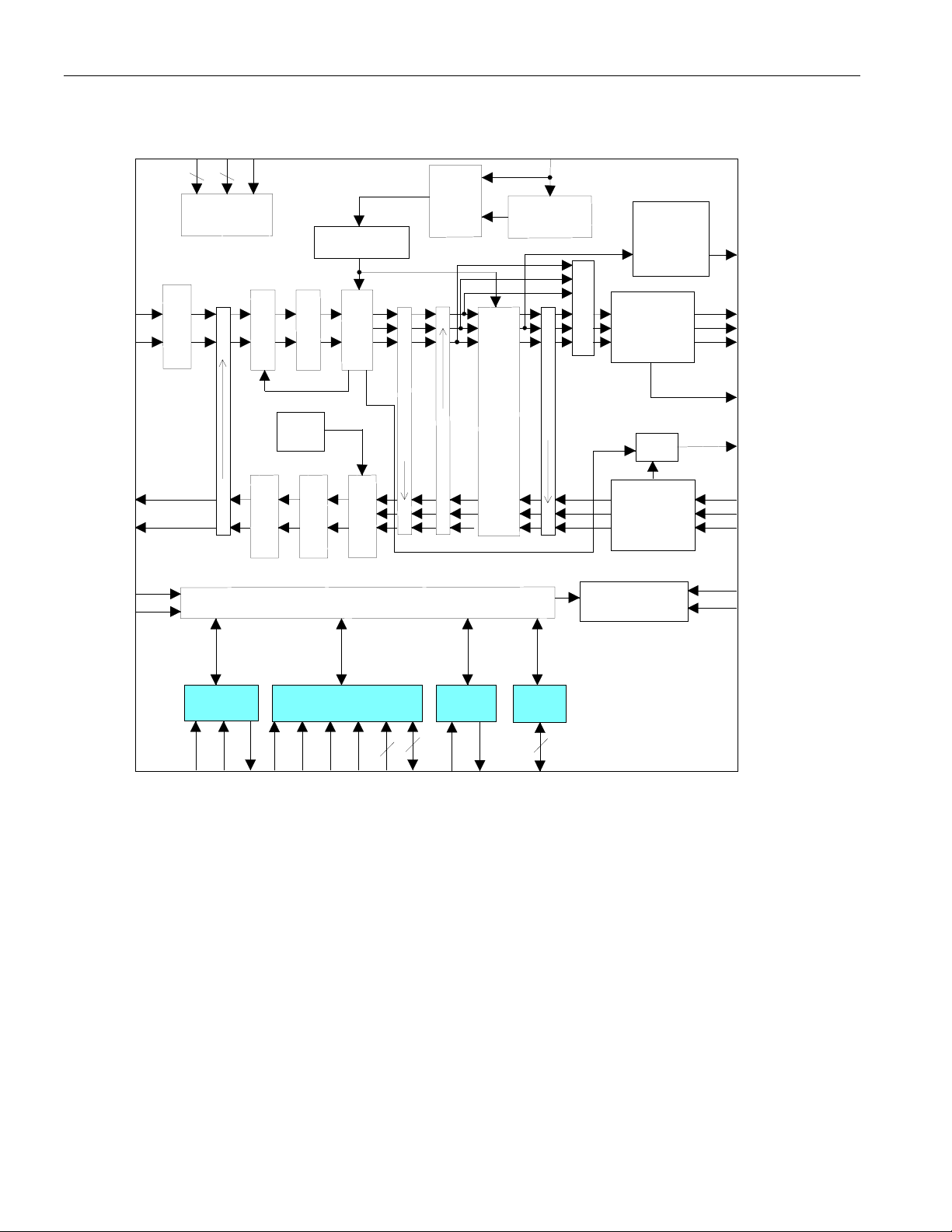
DS21348 BLOCK DIAGRAM Figure 3-1
S
D
S
D
V
2
w
e
o
P
R
N
R
G
I
R
T
P
I
T
N
R
G
I
T
T
P
I
Optional
Termination
VSM
V
2
s
n
o
i
t
c
e
n
n
C
o
r
t
c
e
t
r
e
e
t
D
l
i
k
F
a
e
P
k
c
a
b
p
o
o
L
g
o
l
a
n
A
Unframed
All Ones
Insertion
s
r
e
v
i
r
D
e
n
i
L
s
r
e
t
l
i
F
U
S
C
JACLK
L
L
P
C
/
O
V
a
t
y
a
r
e
D
v
/
o
k
c
c
e
o
l
R
C
g
n
i
p
a
h
S
e
v
a
W
Remote Loopback (Dual Mode)
Jitter
Attenuator
MUX
DS21348/Q348
K
L
C
M
2.048MHz to
1.544MHz PLL
)
h
t
a
p
e
v
i
e
c
e
r
r
o
t
n
i
o
i
t
m
s
a
n
u
a
n
r
t
e
t
t
r
e
A
h
r
k
c
a
b
p
o
o
L
l
a
c
o
L
t
i
e
t
e
t
i
n
J
i
d
e
c
a
l
p
e
b
n
a
c
(
MUX
k
c
a
b
p
o
o
L
e
t
o
m
e
R
16.384MHz or
8.1 92MHz or
4.0 96MHz or
2.048MHz
Synthesizer
See Figure 3-2
MUX RCL/LOTC
See Figure 3-3
BPCLK
RPOS
RCLK
RNEG
PBEO
TPOS
TCLK
TNEG
S
I
B
1
S
I
B
0
U
X
M
r
e
t
r
e
n
I
i
S
l
a
I
K
D
L
S
C
S
l
a
r
e
i
S
e
h
t
(
e
c
a
f
O
S
D
T
S
B
P
n
a
,
l
e
l
l
a
P
,
r
a
r
a
a
P
)
*
W
/
R
(
*
R
W
e
r
H
a
r
w
a
d
d
c
e
l
l
e
r
e
t
a
n
f
I
l
)
)
*
S
S
A
D
(
(
E
*
L
D
A
R
s
r
e
c
t
n
I
5
4
A
o
t
0
A
r
a
f
a
h
s
e
e
C
o
n
I
8
7
/
D
7
A
D
o
o
t
t
0
0
D
D
A
)
i
s
n
v
c
e
d
p
i
e
r
H
a
r
w
a
d
r
t
n
l
o
d
n
a
r
e
t
r
t
p
u
*
*
T
S
N
C
I
e
r
e
c
t
a
n
f
I
e
1
2
r
t
n
l
C
o
o
a
t
d
e
t
u
o
(
r
r
s
o
t
P
t
T
d
e
n
s
c
o
)
k
l
b
l
l
a
o
HRST*
TEST
7 of 73
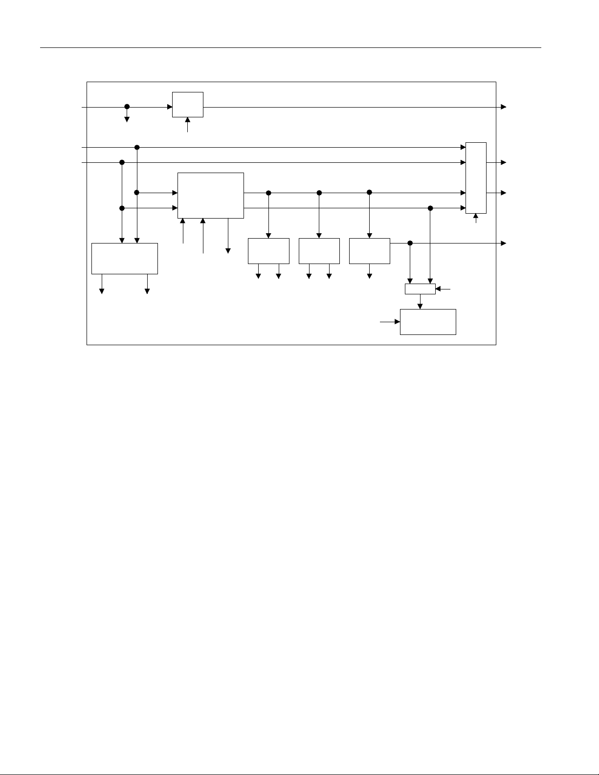
RECEIVE LOGIC Figure 3-2
DS21348/Q348
From
Remote
Loopback
Routed to
All Blocks
4 or 8 Zero Detect
16 Zero Detect
RIR1.7 RIR1.6
Clock
Invert
CCR2.0
CCR2.3
CCR6.2/
CCR6.0/
CCR6.1
B8ZS/HDB3
Decoder
RIR1.5
All Ones
Detector
NRZ Data
BPV/CV/EXZ
Loop Code
Detector
SR.6 SR.7SR.4 RIR1.3
PRBS
Detector
SR.0
CCR1.4
mux
16-Bit Error
Counter (ECR)
RCLK
RPOS
mux
RNEG
CCR1.6
PBEO
CCR6.0
rx bd
8 of 73
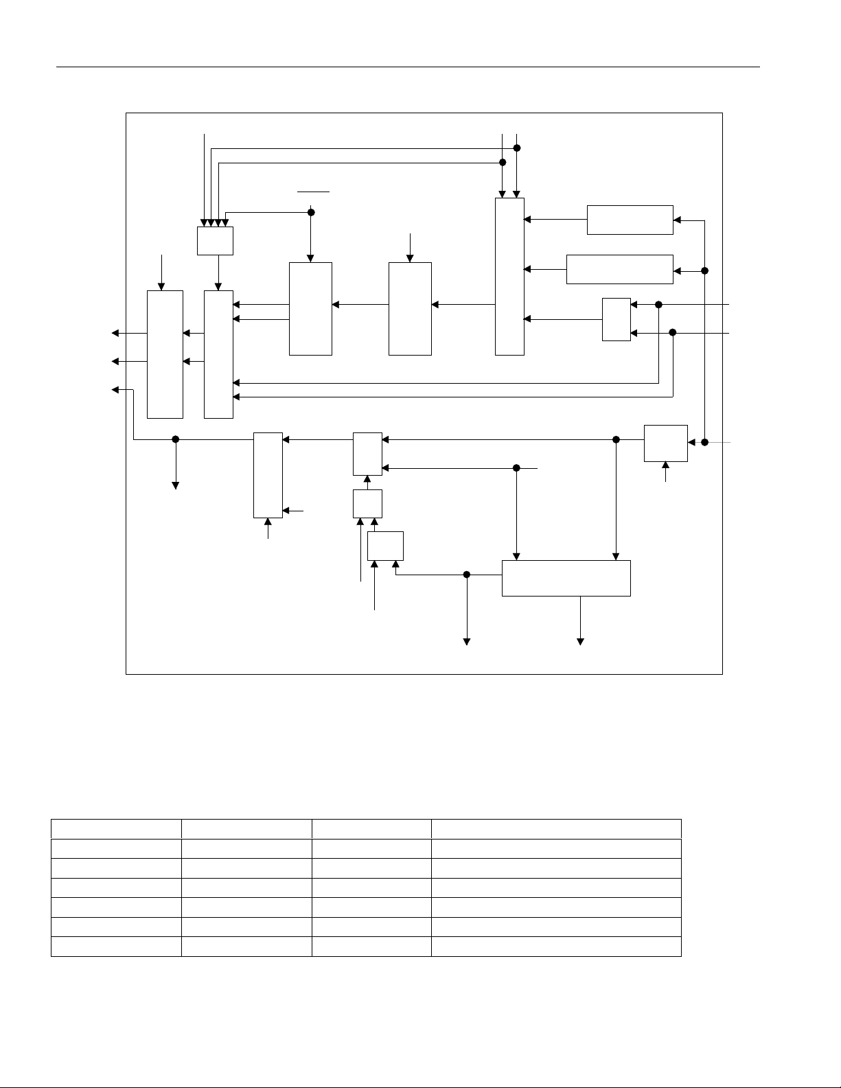
TRANSMIT LOGIC Figure 3-3
DS21348/Q348
To
Remote
Loopback
CCR3.1
BPV
Insert
Routed to
All Blocks
CCR1.6
OR
Gate
mux
mux
CCR3.4
PRBS Generator
Loop Code Generator
JACLK
(derived
from
MCLK)
OR
Gate
Clock
Invert
CCR2.1
TPOS
TNEG
TCLK
CCR3.3
CCR2.2
CCR3.0
1
0
mux
B8ZS/
HDB3
Coder
0
1
RCLK
mux
OR
Gate
0
1
Logic
Error
Insert
CCR1.1
CCR1.2
AND
Gate
CCR1.0
To LOTC Output Pin
Loss Of Transmit
Clock Detect
tx bd
SR.5
4. PIN DESCRIPTION
The DS21348 can be controlled in a parallel port mode, a serial port mode, or a hardware mode (Table
4-1, 4-2, and 4-3). The parallel and serial port modes are described in Section 3, and the Hardware Mode
is described below.
BUS INTERFACE SELECTION Table 4-1
BIS1 BIS0 PBTS MODE
0 0 0 Muxed Intel
0 0 1 Muxed Motorola
0 1 0 Nonmuxed Intel
0 1 1 Nonmuxed Motorola
1 0 - Serial Port
1 1 - Hardware
9 of 73
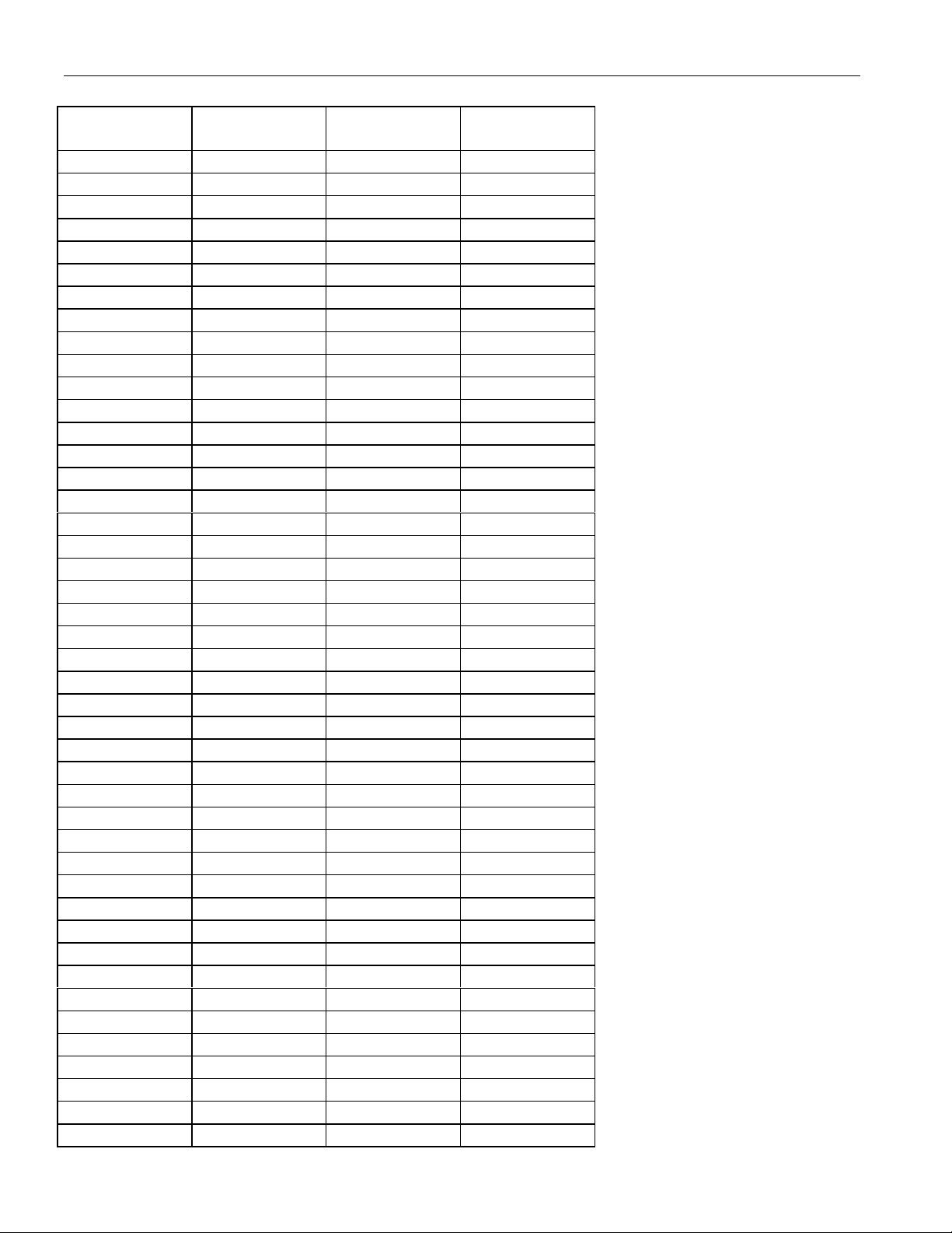
PIN ASSIGNMENT IN PARALLEL PORT MODE Table 4-2a
DS21348T
PIN #
1C3ICS*
2 C2 I RD*(DS*)
3 B1 I WR*(R/W*)
4D2IALE(AS)
5C1INA
6D3INA
7D1I/OA4
8E1IA3
9F2IA2
10 F1 I A1
11 G1 I A0
12 E3 I/O D7/AD7
13 F3 I/O D6/AD6
14 G2 I/O D5/AD5
15 F4 I/O D4/AD4
16 G3 I/O D3/AD3
17 E4 I/O D2/AD2
18 G4 I/O D1/AD1
19 F5 I/O D0/AD0
20 G5 I VSM
21 F6 - V
22 G6 - V
23 E5 I/O INT*
24 E6 O PBEO
25 F7 O RCL/LOTC
26 D6 I TEST
27 D5 I RTIP
28 D7 I RRING
29 C6 I HRST*
30 C7 I MCLK
31 B6 O BPCLK
32 B7 I BIS0
33 A7 I BIS1
34 C5 O TTIP
35 B5 - V
36 A6 - V
37 B4 O TRING
38 C4 O RPOS
39 A4 O RNEG
40 B3 O RCLK
41 A3 I TPOS
42 B2 I TNEG
43 A2 I TCLK
44 A1 I PBTS
DS21348G
PIN#
I/O Parallel
Port Mode
DD
SS
SS
DD
DS21348/Q348
10 of 73

PIN DESCRIPTIONS IN PARALLEL PORT MODE (Sorted by Pin Name,
DS21348T Pin Numbering) Table 4-2b
ACRONYM PIN I/O DESCRIPTION
DS21348/Q348
A0 to A4 11
to
7
I Address Bus. In nonmultiplexed bus operation (BIS1 = 0, BIS0 =
1), serves as the address bus. In multiplexed bus operation (BIS1 =
0, BIS0 = 0), these pins are not used and should be tied low.
ALE(AS) 4 I Address Latch Enable (Address Strobe). When using the parallel
port (BIS1 = 0) in multiplexed bus mode (BIS0 = 0), serves to
demultiplex the bus on a positive-going edge. In nonmultiplexed bus
mode (BIS0 = 1), should be tied low.
BIS0/BIS1 32/33 I Bus Interface Select Bits 0 & 1. Used to select bus interface option.
See Table 4-1 for details.
BPCLK 31 O Back Plane Clock. A 16.384MHz, 8.192MHz, 4.096MHz, or
2.048MHz clock output that is referenced to RCLK selectable via
CCR5.7 and CCR5.6. In hardware mode, defaults to 16.384MHz
output.
CS* 1 I Chip Select. Must be low to read or write to the device. CS* is an
active low signal.
D0 / AD0
to
D7 / AD7
19
to
12
I/O Data Bus/Address/Data Bus. In nonmultiplexed bus operation
(BIS1 = 0, BIS0 = 1), serves as the data bus. In multiplexed bus
operation (BIS1 = 0, BIS0 = 0), serves as an 8-bit multiplexed
address/data bus.
HRST* 29 I Hardware Reset. Bringing HRST* low will reset the DS21348
setting all control bits to their default state of all zeros.
INT* 23 O Interrupt [INT*] Pin 23. Flags host controller during conditions
and change of conditions defined in the Status Register. Active low,
open drain output.
MCLK 30 I Master Clock. A 2.048MHz (±50ppm) clock source with TTL
levels is applied at this pin. This clock is used internally for both
clock/data recovery and for jitter attenuation. Use of a T1 1.544
MHz clock source is optional.
See Note 2.
NA
-INot Assigned. Should be tied low.
PBEO 24 O PRBS Bit Error Output. The receiver will constantly search for a
15
-1 or a 220-1 PRBS depending on the ETS bit setting (CCR1.7).
2
Remains high if out of synchronization with the PRBS pattern. Goes
low when synchronized to the PRBS pattern. Any errors in the
received pattern after synchronization will cause a positive going
pulse (with same period as E1 or T1 clock) synchronous with
RCLK. PRBS bit errors can also be reported to the ECR1 and ECR2
registers by setting CCR6.2 to a logic 1.
PBTS 44 I Parallel Bus Type Select. When using the parallel port (BIS1 = 0),
set high to select Motorola bus timing, set low to select Intel bus
timing. This pin controls the function of the RD*(DS*), ALE(AS),
and WR*(R/W*) pins. If PBTS = 1 and BIS1 = 0, then these pins
assume the Motorola function listed in parenthesis (). In serial port
mode, this pin should be tied low.
11 of 73

ACRONYM PIN I/O DESCRIPTION
DS21348/Q348
RCLK
40 O Receive Clock. Buffered recovered clock from the line.
Synchronous to MCLK in absence of signal at RTIP and RRING.
RD*
(DS*)
2IRead Input (Data Strobe). RD* and DS* are active low signals.
DS active low when in nonmultiplexed, Motorola mode. See the Bus
Timing Diagrams in Section 12.
RCL/
LOTC
25 O Receive Carrier Loss/Loss of Transmit Clock. An output which
will toggle high during a receive carrier loss (CCR2.7 = 0) or will
toggle high if the TCLK pin has not been toggled for 5 msec ± 2
msec (CCR2.7 = 1). CCR2.7 defaults to logic 0 when in hardware
mode.
RNEG
39 O Receive Negative Data. Updated on the rising edge (CCR2.0 = 0)
or the falling edge (CCR2.0 = 1) of RCLK with the bipolar data out
of the line interface. Set NRZE (CCR1.6) to a one for NRZ
applications. In NRZ mode, data will be output on RPOS while a
received error will cause a positive-going pulse synchronous with
RCLK at RNEG. See Section 8.4 for details.
RPOS 38 O Receive Positive Data. Updated on the rising edge (CCR2.0 = 0) or
the falling edge (CCR2.0 = 1) of RCLK with bipolar data out of the
line interface. Set NRZE (CCR1.6) to a one for NRZ applications. In
NRZ mode, data will be output on RPOS while a received error will
cause a positive-going pulse synchronous with RCLK at RNEG. See
Section 8.4 for details.
RTIP/
RRING
27/
28
I Receive Tip and Ring. Analog inputs for clock recovery circuitry.
These pins connect via a 1:1 transformer to the line. See Section 7
for details.
TCLK 43 I Transmit Clock. A 2.048MHz or 1.544MHz primary clock. Used to
clock data through the transmit side formatter. Can be sourced
internally by MCLK or RCLK. See Common Control Register 1 and
Figure 3-3.
TEST 26 I 3-State Control. Set high to 3-state all outputs and I/O pins
(including the parallel control port). Set low for normal operation.
Useful in board level testing.
TNEG 42 I Transmit Negative Data. Sampled on the falling edge (CCR2.1 =
0) or the rising edge (CCR2.1 = 1) of TCLK for data to be
transmitted out onto the line.
TPOS 41 I Transmit Positive Data. Sampled on the falling edge (CCR2.1 = 0)
or the rising edge (CCR2.1 = 1) of TCLK for data to be transmitted
out onto the line.
TTIP/
TRING
34/
37
O Transmit Tip and Ring [TTIP & TRING]. Analog line driver
outputs. These pins connect via a step-up transformer to the line. See
Section 7 for details.
V
DD
21/
- Positive Supply. 5.0V ±5%
36
VSM 20 I Voltage Supply Mode. Should be tied high for 5V operation.
V
SS
22/
-
Signal Ground.
35
12 of 73
ACRONYM PIN I/O DESCRIPTION
DS21348/Q348
WR*
(R/W*)
3IWrite Input (Read/Write). WR* is an active low signal. See the
Bus Timing Diagrams in section 12.
PIN ASSIGNMENT IN SERIAL PORT MODE Table 4-3a
DS21348T
PIN #
1C3ICS*
2C2INA
3B1 INA
4D2INA
5C1ISCLK
6D3ISDI
7D1I/OSDO
8E1 IICES
9F2IOCES
10 F1 I NA
11 G1 I NA
12 E3 I/O NA
13 F3 I/O NA
14 G2 I/O NA
15 F4 I/O NA
16 G3 I/O NA
17 E4 I/O NA
18 G4 I/O NA
19 F5 I/O NA
20 G5 I VSM
21 F6 - VDD
22 G6 - VSS
23 E5 I/O INT*
24 E6 O PBEO
25 F7 O RCL/LOTC
26 D6 I TEST
27 D5 I RTIP
28 D7 I RRING
29 C6 I HRST*
30 C7 I MCLK
31 B6 O BPCLK
32 B7 I BIS0
33 A7 I BIS1
34 C5 O TTIP
35 B5 - V
36 A6 - V
37 B4 O TRING
38 C4 O RPOS
39 A4 O RNEG
DS21348G
PIN#
I/O Serial
Port Mode
SS
DD
13 of 73

DS21348/Q348
DS21348T
PIN #
DS21348G
PIN#
I/O Serial
Port Mode
40 B3 O RCLK
41 A3 I TPOS
42 B2 I TNEG
43 A2 I TCLK
44 A1 I NA
PIN DESCRIPTIONS IN SERIAL PORT MODE (Sorted by Pin Name, DS21348T
Pin Numbering)
ACRONYM PIN I/O DESCRIPTION
Table 4-3b
BIS0/
BIS1
32/
33
I Bus Interface Select Bits 0 & 1. Used to select bus interface option.
See Table 4-1 for details.
BPCLK 31 O Back Plane Clock. A 16.384MHz, 8.192MHz, 4.096MHz, or
2.048MHz clock output that is referenced to RCLK selectable via
CCR5.7 and CCR5.6. In hardware mode, defaults to 16.384 MHz
output.
CS* 1 I Chip Select. Must be low to read or write to the device. CS* is an
active low signal.
HRST* 29 I Hardware Reset. Bringing HRST* low will reset the DS21348
setting all control bits to their default state of all zeros.
ICES
8IInput Clock Edge Select. Selects whether the serial port data input
(SDI) is sampled on rising (ICES =0) or falling edge (ICES = 1) of
SCLK.
INT* 23 O Interrupt [INT*] Pin 23. Flags host controller during conditions
and change of conditions defined in the Status Register. Active low,
open drain output.
MCLK 30 I Master Clock. A 2.048MHz (±50ppm) clock source with TTL
levels is applied at this pin. This clock is used internally for both
clock/data recovery and for jitter attenuation. Use of a T1 1.544
MHz clock source is optional.
See Note 2.
NA
-INot Assigned. Should be tied low.
OCES 9 I Output Clock Edge Select. Selects whether the serial port data
output (SDO) is valid on the rising (OCES = 1) or falling edge
(OCES = 0) of SCLK.
PBEO 24 O PRBS Bit Error Output. The receiver will constantly search for a
15
-1 or a 220-1 PRBS depending on the ETS bit setting (CCR1.7).
2
Remains high if out of synchronization with the PRBS pattern. Goes
low when synchronized to the PRBS pattern. Any errors in the
received pattern after synchronization will cause a positive going
pulse (with same period as E1 or T1 clock) synchronous with
RCLK. PRBS bit errors can also be reported to the ECR1 and ECR2
registers by setting CCR6.2 to a logic 1.
RCLK
40 O Receive Clock. Buffered recovered clock from the line.
Synchronous to MCLK in absence of signal at RTIP and RRING.
14 of 73

ACRONYM PIN I/O DESCRIPTION
DS21348/Q348
RCL/
LOTC
25 O Receive Carrier Loss/Loss of Transmit Clock. An output which
will toggle high during a receive carrier loss (CCR2.7 = 0) or will
toggle high if the TCLK pin has not been toggled for 5 msec ± 2
msec (CCR2.7 = 1). CCR2.7 defaults to logic 0 when in hardware
mode.
RNEG
39 O Receive Negative Data. Updated on the rising edge (CCR2.0 = 0)
or the falling edge (CCR2.0 = 1) of RCLK with the bipolar data out
of the line interface. Set NRZE (CCR1.6) to a one for NRZ
applications. In NRZ mode, data will be output on RPOS while a
received error will cause a positive-going pulse synchronous with
RCLK at RNEG. See section 8.4 for details.
RPOS 38 O Receive Positive Data. Updated on the rising edge (CCR2.0 = 0) or
the falling edge (CCR2.0 = 1) of RCLK with bipolar data out of the
line interface. Set NRZE (CCR1.6) to a one for NRZ applications. In
NRZ mode, data will be output on RPOS while a received error will
cause a positive-going pulse synchronous with RCLK at RNEG. See
section 8.4 for details.
RTIP/
RRING
27/
28
I Receive Tip and Ring. Analog inputs for clock recovery circuitry.
These pins connect via a 1:1 transformer to the line. See Section 7
for details.
SCLK
5ISerial Clock. Serial bus clock input.
SDI 6 I Serial Data Input. Sampled on rising edge (ICES = 0) or the falling
edge (ICES = 1) of SCLK.
SDO 7 O Serial Data Output. Valid on the falling edge (OCES = 0) or the
rising edge (OCES = 1) of SCLK.
TCLK 43 I Transmit Clock. A 2.048MHz or 1.544MHz primary clock. Used to
clock data through the transmit side formatter. Can be sourced
internally by MCLK or RCLK. See Common Control Register 1 and
Figure 3-3.
TEST 26 I 3-State Control. Set high to 3-state all outputs and I/O pins
(including the parallel control port). Set low for normal operation.
Useful in board level testing.
TNEG 42 I Transmit Negative Data. Sampled on the falling edge (CCR2.1 =
0) or the rising edge (CCR2.1 = 1) of TCLK for data to be
transmitted out onto the line.
TPOS 41 I Transmit Positive Data. Sampled on the falling edge (CCR2.1 = 0)
or the rising edge (CCR2.1 = 1) of TCLK for data to be transmitted
out onto the line.
TTIP/
TRING
34/
37
O Transmit Tip and Ring [TTIP & TRING]. Analog line driver
outputs. These pins connect via a step-up transformer to the line.
See Section 7 for details.
V
DD
21/
- Positive Supply. 5.0V ±5%
36
VSM 20 I Voltage Supply Mode. Should be tied high for 5V operation.
V
SS
22/
-
Signal Ground.
35
15 of 73
PIN ASSIGNMENT IN HARDWARE MODE Table 4-4a
DS21348T
PIN #
1C3IEGL
2 C2 I ETS
3B1 INRZE
4D2ISCLKE
5C1I L2
6D3I L1
7D1I/OL0
8E1 IDJA
9F2IJAMUX
10 F1 I JAS
11 G1 I HBE
12 E3 I/O CES
13 F3 I/O TPD
14 G2 I/O TX0
15 F4 I/O TX1
16 G3 I/O LOOP0
17 E4 I/O LOOP1
18 G4 I/O MM0
19 F5 I/O MM1
20 G5 I VSM
21 F6 - VDD
22 G6 - VSS
23 E5 I/O RT1
24 E6 O PBEO
25 F7 O RCL
26 D6 I TEST
27 D5 I RTIP
28 D7 I RRING
29 C6 I HRST*
30 C7 I MCLK
31 B6 O BPCLK
32 B7 I BIS0
33 A7 I BIS1
34 C5 O TTIP
35 B5 - V
36 A6 - V
37 B4 O TRING
38 C4 O RPOS
39 A4 O RNEG
40 B3 O RCLK
41 A3 I TPOS
42 B2 I TNEG
43 A2 I TCLK
44 A1 I RT0
DS21348G
PIN#
I/O Hardware
Mode
SS
DD
DS21348/Q348
16 of 73

DS21348/Q348
PIN DESCRIPTIONS IN HARDWARE MODE (Sorted by Pin Name, DS21348T Pin
Numbering)
ACRONYM PIN I/O DESCRIPTION
Table 4-4b
BIS0/
BIS1
BPCLK 31 O Back Plane Clock. A 16.384MHz, 8.192MHz, 4.096MHz, or
CES
DJA 8 I
EGL 1 I Receive Equalizer Gain Limit. This bit controls the sensitivity of
ETS 2 I
HBE
HRST* 29 I Hardware Reset. Bringing HRST* low will reset the DS21348
JAMUX 9 I Jitter Attenuator MUX. Controls the source for JACLK. See
JAS
L0/L1/L2 7/
LOOP0/
LOOP1
32/
33
12 I Receive & Transmit Clock Edge Select. Selects which RCLK
11 I Receive & Transmit HDB3/B8ZS Enable. HBE combines RHBE
10 I
6/
5
16/
17
I Bus Interface Select Bits 0 & 1. Used to select bus interface option.
See Table 4-1 for details.
2.048MHz clock output that is referenced to RCLK selectable via
CCR5.7 and CCR5.6. In hardware mode, defaults to 16.384MHz
output.
edge to update RPOS and RNEG and which TCLK edge to sample
TPOS and TNEG. CES combines TCES (CCR2.1) and RCES
(CCR2.0).
0 = update RNEG/RPOS on rising edge of RCLK; sample
TPOS/TNEG on falling edge of TCLK
1 = update RNEG/RPOS on falling edge of RCLK; sample
TPOS/TNEG on rising edge of TCLK
Disable Jitter Attenuator.
0 = jitter attenuator enabled
1 = jitter attenuator disabled
the receive equalizer. See Table 4-7.
E1/T1 Select.
0 = E1
1 = T1
(CCR2.3) and THBE (CCR2.2).
0 = enable HDB3 (E1)/B8ZS (T1)
1 = disable HDB3 (E1)/B8ZS (T1)
setting all control bits to their default state of all zeros.
Figure 3-1 and Table 4-10.
0 = JACLK sourced from MCLK (2.048MHz or 1.544MHz at
MCLK)
1 = JACLK sourced from internal PLL (2.048MHz at MCLK)
Jitter Attenuator Select.
0 = place the jitter attenuator on the receive side
1 = place the jitter attenuator on the transmit side
I Transmit LIU Waveshape Select Bits 0 & 1 [H/W Mode]. These
inputs determine the waveshape of the transmitter. See Table 9-1
and Table 9-2.
I Loopback Select Bits 0 & 1 [H/W Mode]. These inputs determine
the active loopback mode (if any). See Table 4-5.
17 of 73

DS21348/Q348
ACRONYM PIN I/O DESCRIPTION
MCLK 30 I Master Clock. A 2.048MHz (±50ppm) clock source with TTL
levels is applied at this pin. This clock is used internally for both
clock/data recovery and for jitter attenuation. Use of a T1 1.544MHz
clock source is optional.
See Note 2.
MM0/
MM1
18/
19
I Monitor Mode Select Bits 0 & 1 [H/W Mode]. These inputs
determine if the receive equalizer is in a monitor mode.
See Table 4-8.
NA
NRZE
-INot Assigned. Should be tied low.
3I
NRZ Enable [H/W Mode].
0 = Bipolar data at RPOS/RNEG and TPOS/TNEG
1 = NRZ data at RPOS and TPOS or TNEG; RNEG outputs a
positive going pulse when device receives a BPV, CV, or EXZ.
PBEO 24 O PRBS Bit Error Output. The receiver will constantly search for a
215-1 or a 220-1 PRBS depending on the ETS bit setting (CCR1.7).
Remains high if out of synchronization with the PRBS pattern.
Goes low when synchronized to the PRBS pattern. Any errors in the
received pattern after synchronization will cause a positive going
pulse (with same period as E1 or T1 clock) synchronous with
RCLK. PRBS bit errors can also be reported to the ECR1 and
ECR2 registers by setting CCR6.2 to a logic 1.
RCLK
40 O Receive Clock. Buffered recovered clock from the line.
Synchronous to MCLK in absence of signal at RTIP and RRING.
RCL 25 O Receive Carrier Loss. An output which will toggle high during a
receive carrier loss (CCR2.7 = 0) or will toggle high if the TCLK
pin has not been toggled for 5 msec ± 2 msec (CCR2.7 = 1). CCR2.7
defaults to logic 0 when in hardware mode.
RNEG
39 O Receive Negative Data. Updated on the rising edge (CCR2.0 = 0)
or the falling edge (CCR2.0 = 1) of RCLK with the bipolar data out
of the line interface. Set NRZE (CCR1.6) to a one for NRZ
applications. In NRZ mode, data will be output on RPOS while a
received error will cause a positive-going pulse synchronous with
RCLK at RNEG. See section 8.4 for details.
RPOS 38 O Receive Positive Data. Updated on the rising edge (CCR2.0 = 0) or
the falling edge (CCR2.0 = 1) of RCLK with bipolar data out of the
line interface. Set NRZE (CCR1.6) to a one for NRZ applications.
In NRZ mode, data will be output on RPOS while a received error
will cause a positive-going pulse synchronous with RCLK at RNEG.
See section 8.4 for details.
RT0/
RT1
RTIP/
RRING
44/
23
27/
28
I Receive LIU Termination Select Bits 0 & 1 [H/W Mode]. These
inputs determine the receive termination. See Table 4-9.
I Receive Tip and Ring. Analog inputs for clock recovery circuitry.
These pins connect via a 1:1 transformer to the line. See Section 7
for details.
18 of 73

ACRONYM PIN I/O DESCRIPTION
DS21348/Q348
SCLKE
4IReceive & Transmit Synchronization Clock Enable. SCLKE
combines RSCLKE (CCR5.3) and TSCLKE (CCR5.2).
0 = disable 2.048 MHz synchronization transmit and receive mode
1 = enable 2.048 MHz synchronization transmit and receive mode
TCLK 43 I Transmit Clock. A 2.048MHz or 1.544MHz primary clock. Used to
clock data through the transmit side formatter. Can be sourced
internally by MCLK or RCLK. See Common Control Register 1 and
Figure 3-3.
TEST 26 I 3-State Control. Set high to 3-state all outputs and I/O pins
(including the parallel control port). Set low for normal operation.
Useful in board level testing.
TNEG 42 I Transmit Negative Data. Sampled on the falling edge (CCR2.1 =
0) or the rising edge (CCR2.1 = 1) of TCLK for data to be
transmitted out onto the line.
TPD
13 I
Transmit Power-Down.
0 = normal transmitter operation
1 = powers down the transmitter and 3-states the TTIP and TRING
pins
TPOS 41 I Transmit Positive Data. Sampled on the falling edge (CCR2.1 = 0)
or the rising edge (CCR2.1 = 1) of TCLK for data to be transmitted
out onto the line.
TTIP/
TRING
34/
37
O Transmit Tip and Ring [TTIP & TRING]. Analog line driver
outputs. These pins connect via a step-up transformer to the line.
See Section 7 for details.
TX0/
TX1
V
DD
14/
15
21/
I Transmit Data Source Select Bits 0 & 1 [H/W Mode]. These
inputs determine the source of the transmit data. See Table 4-6.
- Positive Supply. 5.0V ±5%
36
VSM 20 I Voltage Supply Mode. Should be tied high for 5V operation.
V
SS
22/
-
Signal Ground.
35
NOTES:
1) G.703 requires an accuracy of ±50ppm for both T1 and E1. TR62411 and ANSI specs require an
accuracy of ±32ppm for T1 interfaces.
2) * Denotes active low.
19 of 73
DS21348/Q348
LOOP BACK CONTROL IN HARDWARE MODE Table 4-5
LOOPBACK SYMBOL CONTROL BIT LOOP1 LOOP0
Remote Loop Back RLB CCR6.6 1 1
Local Loop Back LLB CCR6.7 1 0
Analog Loop Back ALB CCR6.4 0 1
No Loop Back - - 0 0
TRANSMIT DATA CONTROL IN HARDWARE MODE Table 4-6
TRANSMIT DATA SYMBOL CONTROL BIT TX1 TX0
Transmit Unframed All Ones TUA1 CCR3.7 1 1
Transmit Alternating Ones and Zeros TAOZ CCR3.5 1 0
Transmit PRBS TPRBSE CCR3.4 0 1
TPOS and TNEG - - 0 0
RECEIVE SENSITIVITY SETTINGS Table 4-7
EGL
(CCR4.4)
0 0 (E1) -12 dB (short haul)
1 0 (E1) -43 dB (long haul)
1 1 (T1) -30 dB (limited long haul)
0 1 (T1) -36 dB (long haul)
ETS
(CCR1.7)
RECEIVE SENSITIVITY
MONITOR GAIN SETTINGS Table 4-8
MM1
(CCR5.5)
0 0 Normal operation (no boost)
01 20
10 26
11 32
MM0
(CCR5.4)
INTERNAL LINEAR GAIN
INTERNAL RX TERMINATION SELECT Table 4-9
RT1
(CCR5.1)
0 0 Internal receive-side termination disabled
01
10
11
RT0
(CCR5.0)
TERMINATION CONFIGURATION
Internal receive-side 120W enabled
Internal receive-side 100W enabled
Internal receive-side 75W
MCLK SELECTION Table 4-10
MCLK JAMUX
(CCR1.3)
2.048MHz 0 0
2.048MHz 1 1
1.544MHz 0 1
BOOST (dB)
INTERNAL RECEIVE
enabled
ETS
(CCR1.7)
20 of 73

PARALLEL PORT MODE PINOUT (BIS1 = 0, BIS0 = 1 or 0) Figure 4-1
34 TTIP
35 VSS
36 VDD
37 TRING
38 RPOS
39 RNEG
40 RCLK
41 TPOS
42 TNEG
43 TCLK
44 PBTS
DS21348/Q348
1 CS*
2 RD (DS)
3 WR* (R/W*)
4 ALE (AS)
5 NA
6 NA
7 A4
8 A3
9 A2
10 A1
11 A0
SERIAL PORT MODE PINOUT (BIS1 = 1, BIS0 = 0) Figure 4-2
AD7/D7 12
tie low
AD6/D6 13
DS21348
Parallel Port
Operation
(Note: tie all NA pins low)
AD2/D2 17
AD3/D3 16
AD4/D4 15
AD5/D5 14
AD1/D1 18
AD0/D0 19
VSM 20
VDD 21
t
i
e
l
o
w
BIS1 33
BIS0 32
BPCLK 31
MCLK 30
HRST* 29
RRING 28
RTIP 27
TEST 26
RCL/LOTC 25
PBEO 24
INT* 23
VSS 22
tie low
tie low (MUX) or high (non-MUX)
1 CS*
2 NA
3 NA
4 NA
5 SCLK
6 SDI
7 SDO
8 ICES
9 OCES
10 NA
11 NA
44 PBTS
NA 12
43 TCLK
41 TPOS
42 TNEG
Serial Port
Operation
(Note: tie all NA pins low)
NA 15
NA 14
NA 13
39 RNEG
40 RCLK
DS21348
NA 16
NA 17
38 RPOS
NA 18
37 TRING
NA 19
VSM 20
34
TT
IP
BPCLK 31
RCL/LOTC 25
VDD 21
VSS 22
BIS1 33
BIS0 32
MCLK 30
HRST* 29
RRING 28
RTIP 27
TEST 26
PBEO 24
INT* 23
tie high
tie low
35 VSS
36 VDD
tie low
21 of 73

HARDWARE MODE PINOUT (BIS1 = 1, BIS0 = 1) Figure 4-3
DS21348/Q348
1 EGL
2 ETS
3 NRZE
4 SCLKE
5 L2
6 L1
7 L0
8 DJA
9 JAMUX
10 JAS
11 HBE
36 VDD
37 TRING
38 RPOS
39 RNEG
40 RCLK
41 TPOS
42 TNEG
43 TCLK
44 RT0
DS21348
Hardware
Operation
LOOP1 17
LOOP0 16
CES 12
TPD 13
TX1 15
TX0 14
MM1 19
MM0 18
VSM 20
tie low
35 VSS
VDD 21
34 TTIP
BIS1 33
BIS0 32
BPCLK 31
MCLK 30
HRST* 29
RRING 28
RTIP 27
TEST 26
RCL 25
PBEO 24
RT1 23
VSS 22
tie high
tie high
5. HARDWARE MODE
In hardware mode (BIS1 = 1, BIS0 = 1), pins 1-19, 23, 25, 31, and 44 are redefined to be used for
initializing the DS21348. BPCLK (pin 31) defaults to a 16.384MHz output when in hardware mode. The
RCL/LOTC (pin 25) is designated to RCL when in hardware mode. JABDS (CCR4.2) defaults to logic 0.
The RHBE (CCR2.3) and THBE (CCR2.2) control bits are combined and controlled by HBE at pin 11
while the RSCLKE (CCR5.3) and TSCLKE (CCR5.2) bits are combined and controlled by SCLKE at
pin 4. TCES (CCR2.1) and RCES (CCR2.0) are combined and controlled by CES at pin 12. The
transmitter functions are combined and controlled by TX1 (pin 15) and TX0 (pin 14). The loopback
functions are controlled by LOOP1 (pin 17) and LOOP0 (pin 16). All other control bits default to the
logic 0 setting.
22 of 73
 Loading...